Advanced Inkjet Capabilities: Challenging Screen-Print Performance. Vahid Akhavan, Ph.D. Senior Application Engineer June 21 st, 2017
|
|
|
- Philippa Joseph
- 5 years ago
- Views:
Transcription

1 Advanced Inkjet Capabilities: Challenging Screen-Print Performance Vahid Akhavan, Ph.D. Senior Application Engineer June 21 st, 2017

2 Company Overview Adding Value Throughout the Printed Electronics Supply Chain INNOVATIONS IN - MATERIALS - PROCESSES - DESIGNS - APPLICATIONS Quick Profile Initially established in 1999 in Austin, TX Privately owned since 2008, as NCC Nano dba NovaCentrix Employees: ~70 in Austin, + 10 in Asia : Facilities: ~ 5800m 2 Extensive IP and know-how related to nanomaterials, conductive inks, and photonic curing

3


4 Temperature Photonic Curing Inks Need high temperature annealing Works best with high absorption and thermally conductive Achieved temperatures much higher than the damage threshold of substrate Thin Film/Substrate Interface Distance from Surface Substrate Thermally Sensitive Works best with light, reflective or transparent materials Best results on thermally resistive substrates


5 Innovation in Post Processing PulseForge 1200/1300 R&D PulseForge 3200/3300 PRODUCTION Different chassis Shared components - Lamps - Reflector housings - Lamp drivers - Power supplies - User interface Rapid and seamless transfer from R&D to Production platform

6 R2R Integration With Inkjet


7 JS-A Based Formulations for Inkjet New aqueous formulation with low boiling point humectants Sintering at 140C Capable of achieving conductivities higher than 20 mω/sqr Improved adhesion and scratchability post photonic curing Evaluated on both Piezoelectric and Thermal inkjet heads Extended lifetime and minimal sedimentation As Deposited Particles Sintering with Photonic Curing
8


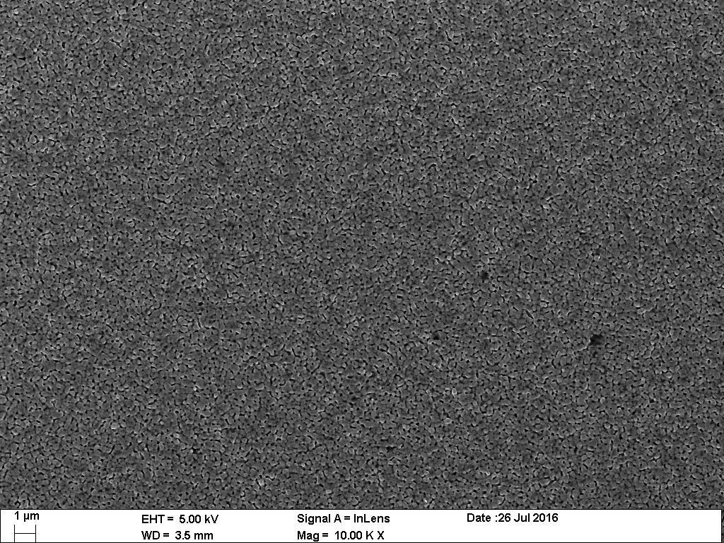
9 Thickness Measurement Prints with DMP 250 µm wide trace at 20 µm drop spacing Visible Image Height Heat Map Cross Section 300 µm wide trace ~ 3 µm height
10 Conductivity Performance of Inkjet Prints With Photonic Curing Melinex ST-505 polyester DMP printer with 10 pl cartridge 20 µm drop spacing 80 C for 10 minutes drying step Photonic curing on PulseForge 1200 Results pass scotch tape test and 5H pencil hardness tests Line definition is maintained
11 Conductivity Performance of Inkjet Prints With Photonic Curing The range of resistance for oven anneal at 120C. The range of resistance for oven at 140C.

12 Multi-layered Films Fully processed on the PulseForge tools Drying Pulse Used 30 µm spacing 17x Sintering Pulse 2x
13 Best Performance To Date JS-A191 Silver Inkjet Ink DMP printer with 10 pl cartridge 20 µm drop spacing Photonic curing on PulseForge 1200 Printing at room temperature All samples pass scratch test All Melinex ST505 samples pass tape test Samples on Polyimide <20 mω/ with PulseForge processing Samples processed at V for 5 ms. Thermal Processing Substrate Cure Temp ( C) Cure Time (min) R S (mω/ ) Melinex ST Polyimide PulseForge Processing Melinex ST505 PulseForge 2.5 J/cm 2 20 Polyimide PulseForge 3.7 J/cm 2 15
14 Cost Competitive The JS-A series inkjet inks are low-cost and high-performance inks. The 20 µm drop spacing prints will be on the order of $ /cm 2. Sample quantities of ink are available at $250/50 ml through our website: store.novacentrix.com With full atomization of the production process, NovaCentrix will sell large volumes of JS-A series inks at $1000/kg. Equivalent conductive performance to silver flake screen ink with low temp thermal curing. Comparable tape and scratch testing to screen printed samples post photonic curing on PET. Volume based discounts are available.
15
16 Summary Introduction of the new JS-A series inks Optimized to be processed through photonic curing Improve material characteristics through photonic curing Demonstrated drying and sintering for this ink with the PulseForge tool Comparable sheet resistance to screen printed circuits Further work is being undertaken to improve component attachment to the printed circuits

17 Contact us with questions or for samples processing. Vahid Akhavan Application Engineer Tel: x201 Stan Farnsworth VP Marketing Tel: x210 Thank You


18 Contact us with questions or for samples processing. Vahid Akhavan Application Engineer Tel: x201 Thank You Stan Farnsworth VP Marketing Tel: x210 Dr. Aoife Celoria is a major contributor to this work. She can be contacted at Aoife.Celoria@novacentrix.com