Discontinuity Regions in Package
|
|
|
- Sharleen Floyd
- 5 years ago
- Views:
Transcription

1 Discontinuity Regions in Package Channel: bonding wire PKG trace via solder ball PCB trace PKG traces & PCB traces: uniform transmission lines Bonding wires, vias & solder balls: discontinuity regions - bandwidths depend on the 3-D structure s design. Bonding Wire PKG Trace Via IC PKG Solder Ball PCB Trace PCB 13
2 Problems by Power/Ground Noise Logic Failure Timing Delay, Skew Power Ground Active Device (IC) IR drop Package SSN Signal Traces PCB or Module Coupling to Signal Line EMI Radiate Emission 14
3 Power/Ground Noise Reduction Method Discrete Decoupling Capacitor on PCB Low Inductance Capacitor on Package Chip Bulk Capacitor VRM Ground Power Chip I Wire Bonding Package P/G Network Ball Bonding PCB P/G Network VRM Decoupling Capacitor On-chip Decoupling Capacitor On Package Decoupling Capacitor On PCB Bulk Capacitor Near VRM Decoupling Capacitors Low Impedance Current Path 15
4 IC-Package-PCB Design and Verification Flow Circuit Design -Schematic Entry Pre-layout Simulation -Design Rule Creation Circuit Design -Schematic Entry Pre-layout Simulation -Design Rule Creation Circuit Design -Schematic Entry Pre-layout Simulation -Design Rule Creation Physical Design -Placement -Routing Post-layout Simulation -SI,PI Verification Physical Design -Placement -Routing Post-layout Simulation -SI,PI Verification Physical Design -Placement -Routing Post-layout Simulation -SI,PI Verification Virtuoso & Spectre APD & HFSS,SIwave Allegro & SIwave System Level IC-Package-PCB PCB Co-simulation Ansoft Designer 16
5 What is different between IC, PKG, and PCB IC PKG PCB 17

6 SIwave Simulation for Plane Capacitance at Center Position PCB PKG IC 18
 DIE Stack_Up ms1 H1=0.09 GND H2=0.1 st1 H3=0.")
7 Test Board Design for Co-simulation Bulk_Cap Power_In SMA Signal_In SMA PWR_A (6cm x 6cm) To Chip - Same Trace Length - Same Wirebond PWR_B (H16mm x V15.3mm) DIE Stack_Up ms1 H1=0.09 GND H2=0.1 st1 H3=0.09 SMA PWR Signal_In 19
 Gate Oxide (t ox ) : 71Å V T : 0.74V R sheet : 3.5 / Die Size : 2.4mm x 2.4mm 169.97 42.71 10.90 2.94 42.49 169.97 2.94 169.75 C total = 778.14pF 2.66 2.")
8 IC Deign for On-chip De-cap Test Chip layout for Verification Hynix 0.25 m m process I/O voltage (V G ) : 3.3V Gate length : 0.34 m (for I/O) Gate Oxide (t ox ) : 71Å V T : 0.74V R sheet : 3.5 / Die Size : 2.4mm x 2.4mm C total = pF No Decap


9 Cell Define Capacitor design Review 21


10 Schematic with Virtuoso of Cadence Inverter 100EA & All Block Schematic 22

11 Layout with Virtuoso of Cadence Inverter 100EA 1 st Inverter 100EA 2 st Inverter 100EA 23

12 2.5V CMOS Inverter with 4 stage of 0.5u, 24
13 Package Design Process with Cadence Tool Allegro Design Entry CIS (schematic) Allegro PCB Editor (layout) Backanotate Schematic Package Schematic Layout Manufacturing Verification Wirebonding Footprint Netlist Stack up Info. Gerber Notice Info. Section Open-Short Test Impedance analysis (coupon) Enviroment setup (Library, Tech File Link) Design spec. fix (Cross-section, Rule Set) Outline, Route Keepin line draw Placement Rule-based Routing Power, Ground Plane draw DRC Check Gerber CAD Flow Design For Manufacturing 25
14 26 Schematic Schematic Package Schematic Layout Schematic Manufacturing Wirebonding Verification Schematic J1 pr_j_via U1 pr_die T1 pr_tantal 1 2 SMA1 pr_sma C1 cap 1 2 B2 BF 1 P1 pr_prove 1 2 Jump_L1 pr_jump 1 2 OUT_VDD


15 Package Schematic Package Schematic Layout ManufacturingVerification Wirebonding 27


16 Schematic Schematic Package Schematic Layout ManufacturingVerification Wirebonding 28


17 Layout Schematic Package Schematic Layout ManufacturingVerification Wirebonding 29

18 Layout (Test Board-A) Test board A Schematic Package Schematic Layout ManufacturingVerification Wirebonding 30


19 Test Board and Wire Bond Test board A Schematic Package Schematic Layout ManufacturingVerification Wirebonding 31

20 PI analysis related to De-cap Value 32
21 PI analysis related to De-cap Value 33


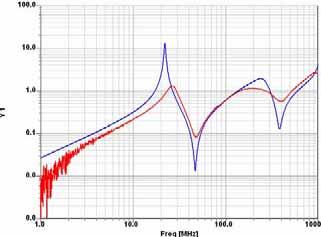
22 Simulation & Measurement Result 34


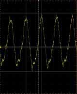


23 Time Domain Measurement vs Simulation 35
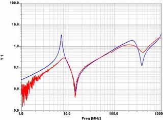
24 PI analysis related to Number of Capacitor 36

25 PI analysis related to Number of Capacitor 37


26 Time Domain Measurement vs Simulation; at 50MHz 1EA 2EA 3EA 4EA 5EA db(z(1,1)) E6 1E7 1E8 1E9 freq, Hz 1E10 38


) 40 20")

27 Time Domain Measurement vs Simulation; at 30MHz 1EA 2EA 3EA 4EA 5EA db(z(1,1)) E6 1E7 1E8 1E9 freq, Hz 1E10 39