Material based challenge and study of 2.1, 2.5 and 3D integration
|
|
|
- Gwendolyn Atkinson
- 5 years ago
- Views:
Transcription
1 1 Material based challenge and study of 2.1, 2.5 and 3D integration Toshihisa Nonaka Packaging Solution Center R&D Headquarters Hitachi Chemical Co., Ltd., Sep. 8, 2016 Hitachi Chemical Co., Ltd All rights reserved.
2 Outline 2 1. Hitachi Chemical Activity - Open Lab.- 2. Cu fine line fabrication regarding 2.1/2.5D 3. In-plane collective bonding with BFL film 4. Study of Vertical collective bonding 5. Summary H.Onozekii

3 HC Production Lineup 3 Dicing Tape Materials for Buffer Coating Interlayer Dielectric Materials Underfill Material Epoxy Molding Compounds CMP Slurry for Cu/Barrier Metal CMP Slurry for STI Die Bonding Film QFN Support tape Die Bonding Paste Photo Sensitive Dry Film High Density Interposer Printed wiring boards Liquid Encapusulant Solder Resist Build-up Materials Package Substrate


4 Activities of Packaging Solution Center Customer demands Customers Propose the total solution 4 Hitachi Chemical Packaging Materials / Adhesion / Elastic modulus / CTE etc. Material Properties Reliability Evaluation Hitachi Chemical Packaging Solution Center / Reflow resistance / TCT resistance / Warpage etc. Current Improvement Initial After MSL2 Initial After MSL2 / Stress Simulation / Warpage FEM : Finite Element Method Structure Analysis Package Assembly / Wafer dicing / D/B, TCB bonding / Mold (Transfer / Compression)
5 Activity of Open Laboratory Supports a materials & process in cooperation with customers Conventional Process New Process (Open Lab.) Material Presentation 5 Submission of Sample (Interaction) Customer s Evaluation Customer s approval Our Sample Offered customer s Device Assemble test in Open Lab. Fix the process condition & Propose the new materials combination / process with customer Customer s approval

 BG (Back grind) BG")
 UF/DCT /")
 FC PCB")


6 Ex. Assembly Scheme in Open Lab. / Flip-chip, 3D, FO-WLP Chip 6 / FO-WLP (300 mm Wafer) Wafer (12inch) BG (Back grind) BG Tape/Temp. film DC (Blade Dicing) UF/DCT / Chip to Substrate / Chip to Chip / Chip to Wafer(300mm) FC PCB (Printed circuit Board) MCL/DFR/SR R/F TCB (Thermal compression bonding) Compres sion Mold MUF EMC RM UF High Accuracy Analyze CUF FC- PKG FC bonder(cow/tcb acceptable) NCP/UF film


7 High Accuracy Analysis Equipment IR Microscope Void Observation 3D X-rays Bump Connection 7 Shadow Moire Warpage &CTE Evaluation Spec Magnification : < X 1,000 Resolution : 0.65 μm 300 / 200 mm wafer SAM Delamination Observation Spec Resolution : < 0.10 μm Magnification : < X 2000 Sample : 508 x 444 mm SEM X-section Spec Sample : 400 X 400 mm Resolution : 3 μm XYZ axis strain and CTE calculation Strain Measuring Equipment Strain Evaluation Spec Sample : 350 x 350 mm Resolution 0.5μm Scan : 1,000 mm / sec Spec Resolution : 3.0 nm Magnification : X 5 ~ X 300,000 Spec Magnification : < X 1,000 Sample size : φ 50 mm, Sample Thickness : 10 mm Temperature : -100 ~ 420 o C

 / Bump pitch ; Min.")
 (Coreless PKG) / DAF thickness : Min. 3 umt / Low CTE & High modulus 32 Die Stack / Coreless prepreg : Min.")
 3 WLP / 12 inch / Mold (Powder, Liquid, Film) (Fan out, Fan in type) / Panel size : Max.")
8 Evaluation Examples for Advanced PKG Table. Evaluation examples for each advanced PKG in Open Lab. 8 No. Items Specification Hitachi chemical materials TEG Image 1 Ultra-fine pitch FC PKG /Silicone & Organic interposer / Low stress underfill (2.1D/2.5D/3D PKG) / L/S=2/2 (w/customer) / RDL (Redistributed dielectrics) Top 4 stacked Bottom die Substrate / Chip to Wafer to Substrate (CoWoS) (Fine patterning, Low Dk type) / Bump pitch ; Min. 40 um / Ultra-low CTE core (CTE : <2ppm) / Dry film resist of fine-pitch (L/S=2/2) / High Tg Solder resist (Liquid/Film) 2 Thin stacked PKC / Die thickness : Min. 15 umt / Prepreg (Min. thickness : 15um) (Coreless PKG) / DAF thickness : Min. 3 umt / Low CTE & High modulus 32 Die Stack / Coreless prepreg : Min. 15 umt Solder resist film / Max. 32 Die stacked / Thin DAF (Thickness : Min. 3-5um) 3 WLP / 12 inch / Mold (Powder, Liquid, Film) (Fan out, Fan in type) / Panel size : Max. 640 x 495mm / Temporary bonding film / RDL first & RDL last process / RDL (Liquid, Film) Panel mold (640x495) Chip (1564 chip) 4 Wearable PKG / Flip-chip assembly to FPC / Low modulus mold materials / Bendable & Expandable (Liquid, Film & High transparency) / Low stress underfill / Low temp. curable conductive paste LED Flip chip (Paste, Film : 150 o C bonding)
9 9 1. Hitachi Chemical Activity - Open Lab.- 2. Cu fine line fabrication regarding 2.1/2.5D 3. In-plane collective bonding with BFL film 4. Study of vertical collective bonding 5. Summary


10 Background of Cu fine line interposer 10 Source: Yole D Fine line oraganic interposer technology is required.

 / (200-250 o C) 18 / 42 ppm/ o C Elastic modulus (40 o C) 11.0 GPa Dk / Df (5GHz) 3.3 / 0.")
11 Evaluation specification of Cu fine line 11 Structure of the test vehicle Si substrate Cu wiring was prepared by Semi-additive process Organic substrate AS500HS AS500HS AS-500HS: Low loss dielectric material Multi Layer structure Primer layer New high-functional resin system Material properties Items Properties Tg (TMA) 201 o C CTE ( o C) / ( o C) 18 / 42 ppm/ o C Elastic modulus (40 o C) 11.0 GPa Dk / Df (5GHz) 3.3 /


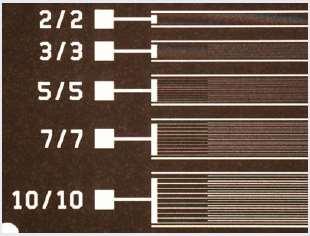
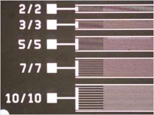
12 Cu fine line fabrication on Si & Organic Sub. 12 Test vehicle Comb electrode L/S-2/2 (mm) Si substrate Organic substrate

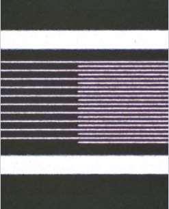
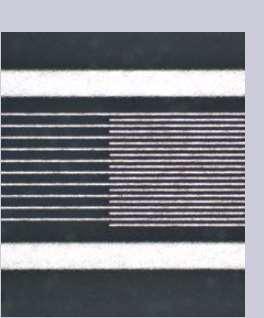
13 Cu fine line fabrication results on Si (Cross section) 13
")
14 Cu fine line fabrication results on Si (Top view) 14

 77 mm (Bottom)")


15 Laser via drilling and b-hast evaluation results 15 Top view of via Cross section of filled via Cu Si AS500HS AS500HS Laser : 355 nm Via diameter: 83 mm (Top) 77 mm (Bottom) b-hast evaluation results of L/S=2/2 mm 130 o C, 85%Rh, 3.3V Microscopic observation results after b-hast Degradation of insulation wasn t observed at 130 o C / 85%Rh for 200 hours.
16 16 1. Hitachi Chemical Activity - Open Lab.- 2. Cu fine line fabrication regarding 2.1/2.5D 3. In-plane collective bonding with BFL film 4. Study of vertical collective bonding 5. Summary

17 Status of 2.5/3D technology 17 Source:Yole D 3D die stacking usually uses TCB (Thermal Compression Bonding). TCB has many advantages in flip chip bonding, The productivity isn t high enough. 2.5/3D technology has been adopted only for high end products. Productivity enhancement of 2.5/3D may contribute to expand the market.
18 Bonding technology for 2.5/3D 18 Thermal compression bonding (TCB) is used for 2.5/3D die stacking TCB process for flip chip bonding. Item TCB process Mass reflow process Fine pitch interconnection Good Fair Warped die assembly Good Poor Productivity Poor Good C4: Mass Reflow Process TCB: Compression Bonding Line process One by one process Improvement of the low productivity is important to meet the various demands of the advanced packages like 2.5 and 3D multi die stacking.


19 How to enhance TCB productivity? 19 One die bonding by one process Plural die bonding by one process Bonding type Process image Concern Material solution In-plane collective Height deviation of bump and pad Substrate topology BFL (bonding force leveling) Film Vertical collective Temperature deviation among dies High thermal conductive material 3D collective Height deviation of bump and pad Substrate topology Temperature deviation among dies Combination of above 2?
20 Improvement of productivity in TCB process 20 Conventional TCB process Die TCB TCB head The die by die sequential process steps Die pick up Pre-bonding Substrate In-plane collective bonding Die placement Mounter head Main bonding Head cooling The improvement process of productivity Die pick up Large TCB head In-plane collective TCB Pre-bonding Multi dies main bonding

21 The concern of in-plane collective bonding 21 Die shift Less bonding force There are unevennesses of bump height and pad thickness, unflatness of substrate surface and unparallelism of bonding head to the stage. Those may cause the die shift and the less bonding force.
22 Idea of bonding force leveling (BFL) film 22 A conventional in plane collective bonding The die placement Mounter head In-plane collective bonding with BFLfilm In plane collective bonding Large TCB head Bonding force leveling film The difference in level on dies The eliminating difference in level on dies The new film inserted between the head and the dies can level the applied bonding force among the multi pre-placed dies.
 Bump height: 16 μm Method & condition Analysis method : FEM analysis Elastic-plastic Simulation Head Stage")
23 Simulation study of leveling performance (model) 23 Items Evaluation of leveling performance of insertion film by smashed Au bump. Model Die size: 7.3 mm x 7.3 mm Die thickness: 300 μm Bump: Plated Au Bump count: 544 Bump pitch: 50 μm (peripheral) Bump height: 16 μm Method & condition Analysis method : FEM analysis Elastic-plastic Simulation Head Stage Die 10 μm Film Au bump The head was inclined to one corner which was 10 μm lower than the diagonal corner. Bonding force :0-100N (vertical direction) Film Head (Rigid body) Die Si E=183 GPa Au bump E=75 GPa (Yield stress=180 MPa) Various types of the films were evaluated.

24 Simulation Results of leveling performance 24 Film Without film Thermoplastic resin film Thermosetting resin film Modulus of film (at 25 o C) MPa 1.0 GPa Model of Contact Head Die Head Die Film Head Die Film Deformation of Au bump The maximum difference 7.8 μm 7.0 μm 1.9 μm : The position of head was inclined to one corner which was 10 μm lower than the diagonal corner. The thermosetting resin film insertion was very effective to the leveling of the bonding force.
25 Function thermosetting BFL film 25 Large TCB head BFL film Unevenness Unparallelism The BFL film is set up between the head and the dies which are pre placed on the substrate. Firstly, the compensating the height difference among the dies where the thermosetting resin layer melts and flows, and then cured Next, the multi die bonding where the bonding force is applied through the cured resin layer to change the shape of the resin to fit each die height.
 Bump height: 16 μm Au bump Die Bonding head was inclined to one corner which was 10 μm lower than the diagonal corner.")
26 The bonding force leveling effect by BFL film 26 Head Stage Die Film Au bump 10 μm Die size: 7.3 mm x 7.3 mm Die thickness: 300 μm Bump: Au plated Bump pitch: 50 μm (peripheral) Bump height: 16 μm Au bump Die Bonding head was inclined to one corner which was 10 μm lower than the diagonal corner.* 1 Die was forced to the stage by the head at 260 o C for 5s. Film Without film PTEF film BFL film (Thermosetting resin layer) Smashed bump height *1 Maximum difference 9.3 μm 7.1 μm 3.5 μm The film less press reflected the incline of the head to the bump height. The insertion of BFL film made the bump height deviation smaller than that of PTFE film.
 Bump height: 16 μm Au bump Die A B Au bump Die Die was forced by the head to the stage at 260 o C for 5s.")
27 Difference of bump height (μm) The effect of the elastic modulus of thermosetting resin layer on BFL 27 Head Stage Die 5 types of the cured BFL film which had different elastic modulus Au bump Die size: 7.3 mm x 7.3 mm Die thickness: 300 μm Bump: Plated Au Bump pitch: 50 μm (peripheral) Bump height: 16 μm Au bump Die A B Au bump Die Die was forced by the head to the stage at 260 o C for 5s. Observed difference of bump height = A - B (The density of Au bump is different from A in B) E E E E E+10 Elastic modulus (Pa) Elastic modulus of the cured thermosetting resin layer has higher bonding force leveling performance.

28 In-plane collective bonding experiment 28 Bonding condition Methods of Bonding Bonding force Bonding temperature Stage temperature Die placement Pulse heat Multi bonding 1st step 2nd step Die placement Constant heat Multi bonding N/die s o C s o C Equipment Die placement: LFB-2301 (Shinkawa Ltd.) Multi dies main bonding: HTB-MM (Alpha Design Co., Ltd) Bonding head temperature: max. 450 o C (Pulse heating) max. 300 o C (Constant heating) Bonding force: 100 N N Head size: 60 mm x 70 mm (Pulse heating) 100 mm x 100 mm (Constant heating) HTB-MM

 + 300 μm (Core")

 (B) (E) 15 dies on a single substrate")
29 Set up of in-plane collective bonding 29 Die size: 7.3 mm x 7.3 mm Die thickness: 100 μm Bump: Cu pillar Bump pitch: 80 μm (Peripheral) μm (Core area) Bump height: 45 μm Cu trace of substrate: 15 μm Substrate thickness: 0.36 mm 5 singulated die and substrate (D) (A) (C) (B) (E) 15 dies on a single substrate Pulse heating (A) (C) (B) (D) (E) Constant heating


30 In-plane collective bonding with BFL film <5 dies of singulated test vehicles> 30 Item Without film PTFE film BFL film Daisy chain test (NG/Total) 0/5 0/5 0/5 Die shift of the bonding Average of die shift 14.0 μm 11.1 μm 3.1 μm Void Void C-SAM observation of die A The BFL film shows good performance not only in the daisy chain test, but also die shift and C-SAM observation.
 14/15")


31 In-plane collective bonding with BFL film <15 dies on a single substrate > 31 Item Without film PTFE film BFL film Daisy chain test (NG/Total) 14/15 7/15 0/15 Die shift of the bonding Average of die shift 29.4 μm 26.6 μm 5.3 μm C-SAM observation of die A Void The BFL film suppressed the die shift more effectively than the others at 15 dies collective bonding. The through put of the process based on the main bonding condition was calculated to be 2700 UPH.
32 32 Thank you for attention!

33 33 The entry contents of these data based on the results of our experiment done until April do not guarantee their characteristic values. The contents may be revised according to new findings if necessary. Please examine the process and the condition carefully and SEMICON confirm before Taiwan mass production. 2016
Novel Materials and Activities for Next Generation Package. Hitachi Chemical., Co.Ltd. Packaging Solution Center Hiroaki Miyajima
 Novel Materials and Activities for Next Generation Package Hitachi Chemical., Co.Ltd. Packaging Solution Center Hiroaki Miyajima 1. Activities of Packaging Solution Center 2. Novel Materials for Next Gen.
IME Technical Proposal. High Density FOWLP for Mobile Applications. 22 April High Density FOWLP Consortium Forum
 IME Technical Proposal High Density FOWLP for Mobile Applications 22 April 2014 Packaging driver for portable / mobile applications Key drivers/needs Smaller form-factor lower profile, substrate-less Higher
Henkel Enabling Materials for Semiconductor and Sensor Assembly. TechLOUNGE, 14 November 2017
 Henkel Enabling Materials for Semiconductor and Sensor Assembly TechLOUNGE, 14 November 2017 Content Brief HENKEL Introduction and ELECTRONICS Focus Areas Innovative Semiconductor and Sensor Assembly Solutions
An Innovative High Throughput Thermal Compression Bonding Process
 An Innovative High Throughput Thermal Compression Bonding Process Li Ming 2 September 2015 Outline Introduction Throughput improved TCB Process Liquid Phase Contact (LPC) bonding Flux-LPC-TCB under inert
Chips Face-up Panelization Approach For Fan-out Packaging
 Chips Face-up Panelization Approach For Fan-out Packaging Oct. 15, 2015 B. Rogers, D. Sanchez, C. Bishop, C. Sandstrom, C. Scanlan, TOlson T. REV A Background on FOWLP Fan-Out Wafer Level Packaging o Chips
3D Package Technologies Review with Gap Analysis for Mobile Application Requirements. Apr 22, 2014 STATS ChipPAC Japan
 3D Package Technologies Review with Gap Analysis for Mobile Application Requirements Apr 22, 2014 STATS ChipPAC Japan T.Nishio Contents Package trends and roadmap update Advanced technology update Fine
SLIM TM, High Density Wafer Level Fan-out Package Development with Submicron RDL
 2017 IEEE 67th Electronic Components and Technology Conference SLIM TM, High Density Wafer Level Fan-out Package Development with Submicron RDL YoungRae Kim 1, JaeHun Bae 1, MinHwa Chang 1, AhRa Jo 1,
Copyright 2009 Year IEEE. Reprinted from 2009 Electronic Components and Technology Conference. Such permission of the IEEE does not in any way imply
 Copyright 2009 Year IEEE. Reprinted from 2009 Electronic Components and Technology Conference. Such permission of the IEEE does not in any way imply IEEE endorsement of any of Institute of Microelectronics
Challenges and Solutions for Cost Effective Next Generation Advanced Packaging. H.P. Wirtz, Ph.D. MiNaPAD Conference, Grenoble April 2012
 Challenges and Solutions for Cost Effective Next Generation Advanced Packaging H.P. Wirtz, Ph.D. MiNaPAD Conference, Grenoble April 2012 Outline Next Generation Package Requirements ewlb (Fan-Out Wafer
Avatrel Stress Buffer Coatings: Low Stress Passivation and Redistribution Applications
 Avatrel Stress Buffer Coatings: Low Stress Passivation and Redistribution Applications Ed Elce, Chris Apanius, Jeff Krotine, Jim Sperk, Andrew Bell, Rob Shick* Sue Bidstrup-Allen, Paul Kohl Takashi Hirano,
Cu Pillar Interconnect and Chip-Package-Interaction (CPI) for Advanced Cu Low K chip
 for Advanced Cu Low K chip") EPRC 12 Project Proposal Cu Pillar Interconnect and Chip-Package-Interaction (CPI) for Advanced Cu Low K chip 15 th Aug 2012 Page 1 Introduction: Motivation / Challenge Silicon device with ultra low k
EPRC 12 Project Proposal Cu Pillar Interconnect and Chip-Package-Interaction (CPI) for Advanced Cu Low K chip 15 th Aug 2012 Page 1 Introduction: Motivation / Challenge Silicon device with ultra low k
Development and Characterization of 300mm Large Panel ewlb (embedded Wafer Level BGA)
") Development and Characterization of 300mm Large Panel ewlb (embedded Wafer Level BGA) Seung Wook Yoon, Yaojian Lin and Pandi C. Marimuthu STATS ChipPAC Ltd. 5 Yishun Street 23, Singapore 768442 E-mail
Development and Characterization of 300mm Large Panel ewlb (embedded Wafer Level BGA) Seung Wook Yoon, Yaojian Lin and Pandi C. Marimuthu STATS ChipPAC Ltd. 5 Yishun Street 23, Singapore 768442 E-mail
TSV CHIP STACKING MEETS PRODUCTIVITY
 TSV CHIP STACKING MEETS PRODUCTIVITY EUROPEAN 3D TSV SUMMIT 22-23.1.2013 GRENOBLE HANNES KOSTNER DIRECTOR R&D BESI AUSTRIA OVERVIEW Flip Chip Packaging Evolution The Simple World of C4 New Flip Chip Demands
IMPLEMENTATION OF A FULLY MOLDED FAN-OUT PACKAGING TECHNOLOGY
 IMPLEMENTATION OF A FULLY MOLDED FAN-OUT PACKAGING TECHNOLOGY B. Rogers, C. Scanlan, and T. Olson Deca Technologies, Inc. Tempe, AZ USA boyd.rogers@decatechnologies.com ABSTRACT Fan-Out Wafer-Level Packaging
Panel Discussion: Advanced Packaging
 Dr. Steve Bezuk Senior Director IC Packaging Engineering Qualcomm Technologies, Inc. Panel Discussion: Advanced Packaging PAGE 1 Technical Challenges of Packaging (Mobile Focus) Materials Die materials
TGV and Integrated Electronics
 TGV and Integrated Electronics Shin Takahashi ASAHI GLASS CO., LTD. 1 Ambient Intelligence Green Energy/Environment Smart Factory Smart Mobility Smart Mobile Devices Bio/Medical Security/Biometrics 2 Glass
Die Attach Materials. Die Attach G, TECH. 2U. TECHNICAL R&D DIV.
 Die Attach Materials Die Attach G, TECH. 2U. TECHNICAL R&D DIV. 2 Topics 3 What it is X 5,000 X 10,000 X 50,000 Si Chip Au Plating Substrate Ag Resin 4 Current Products Characteristics H9890-6A H9890-6S
3D-IC Integration using D2C or D2W Alignment Schemes together with Local Oxide Reduction
 3D-IC Integration using D2C or D2W Alignment Schemes together with Local Oxide Reduction Gilbert Lecarpentier*, Jean-Stéphane Mottet* SET S.A.S. (Smart Equipment Technology), 131 Impasse Barteudet, 74490
Recent Advances in Die Attach Film
 Recent Advances in Die Attach Film Frederick Lo, Maurice Leblon, Richard Amigh, and Kevin Chung. AI Technology, Inc. 70 Washington Road, Princeton Junction, NJ 08550 www.aitechnology.com Abstract: The
Molding materials performances experimental study for the 3D interposer scheme
 Minapad 2014, May 21 22th, Grenoble; France Molding materials performances experimental study for the 3D interposer scheme Y. Sinquin, A. Garnier, M. Argoud, A. Jouve, L. Baud, J. Dechamp, N. Allouti,
Encapsulation Materials Technology For SiP in Automotive
 Encapsulation Materials Technology For SiP in Automotive Oct. 17. 2018 Panasonic Corporation Electronic Materials Business Division Our Business Fields Electronic Instruments Networking equipment Smart
5. Packaging Technologies Trends
 5. Packaging Technologies Trends Electronic products and microsystems continue to find new applications in personal, healthcare, home, automotive, environmental and security systems. Advancements in packaging
S/C Packaging Assembly Challenges Using Organic Substrate Technology
 S/C Packaging Assembly Challenges Using Organic Substrate Technology Presented by Bernd Appelt ASE Group Nov. 17, 2009 Overview The Packaging Challenge Chip Substrate Interactions Stiffeners for FC-BGA
3DIC Integration with TSV Current Progress and Future Outlook
 3DIC Integration with TSV Current Progress and Future Outlook Shan Gao, Dim-Lee Kwong Institute of Microelectronics, A*STAR (Agency for Science, Technology and Research) Singapore 9 September, 2010 1 Overview
Challenges of Fan-Out WLP and Solution Alternatives John Almiranez
 Challenges of Fan-Out WLP and Solution Alternatives John Almiranez Advanced Packaging Business Development Asia Introduction to Fan-Out WLP Introduction World of mobile gadgetry continues to rapidly evolve
WF6317. A superactive low-volatile/high heat-resistant water-soluble flux for ball soldering
 WF637 A superactive low-volatile/high heat-resistant water-soluble flux for ball soldering Low viscosity and high tacking power stabilize ball holding force and ensures excellent solder wettability Easy
IME Proprietary. EPRC 12 Project Proposal. 3D Embedded WLP. 15 th August 2012
 EPRC 12 Project Proposal 3D Embedded WLP 15 th August 2012 Motivation Factors driving IC market Higher density, lower cost, high yield Fan-out WLP/eWLP advantages Small footprint, low profile Low cost,
23 rd ASEMEP National Technical Symposium
 THE EFFECT OF GLUE BOND LINE THICKNESS (BLT) AND FILLET HEIGHT ON INTERFACE DELAMINATION Raymund Y. Agustin Janet M. Jucar Jefferson S. Talledo Corporate Packaging & Automation/ Q&R STMicroelectronics,
Mechanical Behavior of Flip Chip Packages under Thermal Loading
 Mechanical Behavior of Flip Packages under Thermal Loading *Shoulung Chen 1,2, C.Z. Tsai 1,3, Nicholas Kao 1,4, Enboa Wu 1 1 Institute of Applied Mechanics, National Taiwan University 2 Electronics Research
Henkel Adhesive Solutions for SiP Packaging. October 17-19, 2018 Shanghai, China
 Henkel Adhesive Solutions for SiP Packaging October 17-19, 2018 Shanghai, China Agenda 1 2 3 4 Overview: Henkel Adhesive Electronics Semiconductor Market Trends & SiP Drivers Henkel Adhesive Solutions
II. A. Basic Concept of Package.
 Wafer Level Package for Image Sensor Module Won Kyu Jeung, Chang Hyun Lim, Jingli Yuan, Seung Wook Park Samsung Electro-Mechanics Co., LTD 314, Maetan3-Dong, Yeongtong-Gu, Suwon, Gyunggi-Do, Korea 440-743
Next Gen Packaging & Integration Panel
 Next Gen Packaging & Integration Panel ECTC 2012 Daniel Tracy, Sr. Director Industry Research & Statistics SEMI May 29, 2012 Packaging Supply Chain Market Trends Material Needs and Opportunities Market
First Demonstration of Panel Glass Fan-out (GFO) Packages for High I/O Density and High Frequency Multi-Chip Integration
 Packages for High I/O Density and High Frequency Multi-Chip Integration") 2017 IEEE 67th Electronic Components and Technology Conference First Demonstration of Panel Glass Fan-out (GFO) Packages for High I/O Density and High Frequency Multi-Chip Integration Tailong Shi, Chintan
2017 IEEE 67th Electronic Components and Technology Conference First Demonstration of Panel Glass Fan-out (GFO) Packages for High I/O Density and High Frequency Multi-Chip Integration Tailong Shi, Chintan
Innovative Substrate Technologies in the Era of IoTs
 Innovative Substrate Technologies in the Era of IoTs Dyi- Chung Hu 胡迪群 September 4, 2015 Unimicron Contents Introduction Substrate Technology - Evolution Substrate Technology - Revolution Glass substrate
Two Chips Vertical Direction Embedded Miniaturized Package
 Two Chips Vertical Direction Embedded Miniaturized Package Shunsuke Sato, 1 Koji Munakata, 1 Masakazu Sato, 1 Atsushi Itabashi, 1 and Masatoshi Inaba 1 Continuous efforts have been made to achieve seemingly
Outline. Market Size Industry Trends Material Segment Trends China Summary. Packaging Materials Market Trends, Issues and Opportunities
 Packaging Materials Market Trends, Issues and Opportunities Dan Tracy Sr. Director Industry Research SEMI 8 th December 2015 Outline Market Size Industry Trends Material Segment Trends China Summary 1
3D-WLCSP Package Technology: Processing and Reliability Characterization
 3D-WLCSP Package Technology: Processing and Reliability Characterization, Paul N. Houston, Brian Lewis, Fei Xie, Ph.D., Zhaozhi Li, Ph.D.* ENGENT Inc. * Auburn University ENGENT, Inc. 2012 1 Outline Packaging
Packaging Effect on Reliability for Cu/Low k Damascene Structures*
 Packaging Effect on Reliability for Cu/Low k Damascene Structures* Guotao Wang and Paul S. Ho Laboratory of Interconnect & Packaging, TX 78712 * Work supported by SRC through the CAIST Program TRC 2003
Challenges for Embedded Device Technologies for Package Level Integration
 Challenges for Embedded Device Technologies for Package Level Integration Kevin Cannon, Steve Riches Tribus-D Ltd Guangbin Dou, Andrew Holmes Imperial College London Embedded Die Technology IMAPS-UK/NMI
BGA Package Underfilm for Autoplacement. Jan Danvir Tom Klosowiak
 BGA Package Underfilm for Autoplacement Jan Danvir Tom Klosowiak NIST-ATP Acknowledgment Project Brief Microelectronics Manufacturing Infrastructure (October 1998) Wafer-Scale Applied Reworkable Fluxing
Ultralow Residue Semiconductor Grade Fluxes for Copper Pillar Flip-Chip
 Ultralow Residue Semiconductor Grade Fluxes for Copper Pillar Flip-Chip SzePei Lim (Presenter), Jason Chou, Maria Durham, and Dr. Andy Mackie Indium Corporation 1 Outline of Presentation Roadmaps and challenges
MEPTEC Semiconductor Packaging Technology Symposium
 MEPTEC Semiconductor Packaging Technology Symposium Advanced Packaging s Interconnect Technology Process Shift and Direction October 23, 2014 Jay Hayes- Director of Business Development -Bumping and Flip
Nanium Overview. Company Presentation
 Nanium Overview Company Presentation Nanium Overview Our name and logo nano prefix of Greek origin referring to small objects ium suffix of Latin origin that includes the formation of scientific terms
Anisotropic Conductive Films (ACFs)
") Anisotropic Conductive Films (ACFs) ACF = Thermosetting epoxy resin film + Conductive particles Chip or substrate 1 Heat Pressure ACF Substrate 2 Chip or substrate 1 ACF Substrate 2 Applications Chip-on-Board
Anisotropic Conductive Films (ACFs) ACF = Thermosetting epoxy resin film + Conductive particles Chip or substrate 1 Heat Pressure ACF Substrate 2 Chip or substrate 1 ACF Substrate 2 Applications Chip-on-Board
Wafer Level Molded DDFN Package Project Duane Wilcoxen
 Wafer Level Molded DDFN Package Project Duane Wilcoxen Definition of DDFN (Encapsulated CSP) DDFN package basically is a CSP device with an epoxy coating on all (or most) of the device sides for added
Narrowing the Gap between Packaging and System
 Narrowing the Gap between Packaging and System Meptec Symposium 2015 ASE (US) Inc Ou Li Nov 10 th, 2015 Outline Industry Dynamics The Need for System Integrators IC/Pkg/System Collaboration Summary 2 Market
PoP/CSP Warpage Evaluation and Viscoelastic Modeling
 PoP/CSP Warpage Evaluation and Viscoelastic Modeling Wei Lin, Min Woo Lee Amkor Technology 19 S Price Rd, Chandler, AZ 85286 wlin@amkor.com Abstract The purpose of this paper was to evaluate the critical
Development of Super Thin TSV PoP
 Development of Super Thin TSV PoP by Seung Wook Yoon, *Kazuo Ishibashi, Shariff Dzafir, Meenakshi Prashant, Pandi Chelvam Marimuthu and **Flynn Carson STATS ChipPAC Ltd. 5 Yishu n Street 23, Singapore
Cost effective 300mm Large Scale ewlb (embedded Wafer Level BGA) Technology
 Technology") Cost effective 300mm Large Scale ewlb (embedded Wafer Level BGA) Technology by Meenakshi Prashant, Seung Wook Yoon, Yaojian LIN and Pandi C. Marimuthu STATS ChipPAC Ltd. 5 Yishun Street 23, Singapore 768442
Cost effective 300mm Large Scale ewlb (embedded Wafer Level BGA) Technology by Meenakshi Prashant, Seung Wook Yoon, Yaojian LIN and Pandi C. Marimuthu STATS ChipPAC Ltd. 5 Yishun Street 23, Singapore 768442
Warpage Mechanism of Thin Embedded LSI Packages
 Nakashima et al.: Warpage Mechanism of Thin Embedded LSI Packages (1/10) [Technical Paper] Warpage Mechanism of Thin Embedded LSI Packages Yoshiki Nakashima*, Katsumi Kikuchi*, Kentaro Mori*, Daisuke Ohshima**,
Glass Carrier for Fan Out Panel Level Package
 January 25, 2018 NEWS RELEASE Development of HRDP TM Material for Formation of Ultra-Fine Circuits with Glass Carrier for Fan Out Panel Level Package - Aiming for mass production in collaboration with
Interconnection Reliability of HDI Printed Wiring Boards
 Presented in the ECWC 10 Conference at IPC Printed Circuits Expo, SMEMA Council APEX and Designers Summit 05 Interconnection Reliability of HDI Printed Wiring Boards Tatsuo Suzuki Nec Toppan Circuit Solutions,
Simulations and Characterizations for Stress Reduction Designs in Wafer Level Chip Scale Packages
 Simulations and Characterizations for Stress Reduction Designs in Wafer Level Chip Scale Packages by Ming-Che Hsieh STATS ChipPAC Taiwan Co. Ltd. Copyright 2013. Reprinted from 2013 International Microsystems,
Modelling Embedded Die Systems
 Modelling Embedded Die Systems Stoyan Stoyanov and Chris Bailey Computational Mechanics and Reliability Group (CMRG) University of Greenwich, London, UK 22 September 2016 IMAPS/NMI Conference on EDT Content
Fraunhofer IZM Bump Bonding and Electronic Packaging
 Fraunhofer IZM Bump Bonding and Electronic Packaging Fraunhofer Institute for Reliability and Microintegration (IZM) Gustav-Meyer-Allee 25 13355 Berlin Germany Dipl.-Ing. Thomas Fritzsch Contact: thomas.fritzsch@izm.fraunhofer.de
Board Level Reliability Improvement in ewlb (Embedded Wafer Level BGA) Packages
 Packages") Board Level Reliability Improvement in ewlb (Embedded Wafer Level BGA) Packages by Seng Guan Chow, Yaojian Lin, Bernard Adams * and Seung Wook Yoon** STATS ChipPAC Ltd. 5 Yishun Street 23, Singapore 768442
Board Level Reliability Improvement in ewlb (Embedded Wafer Level BGA) Packages by Seng Guan Chow, Yaojian Lin, Bernard Adams * and Seung Wook Yoon** STATS ChipPAC Ltd. 5 Yishun Street 23, Singapore 768442
Flip Chip - Integrated In A Standard SMT Process
 Flip Chip - Integrated In A Standard SMT Process By Wilhelm Prinz von Hessen, Universal Instruments Corporation, Binghamton, NY This paper reviews the implementation of a flip chip product in a typical
Wire-Bond CABGA A New Near Die Size Packaging Innovation Yeonho Choi February 1, 2017
 Amkor Technology, Inc. White Paper Wire-Bond CABGA A New Near Die Size Packaging Innovation Yeonho Choi February 1, 2017 Abstract Expanding its ChipArray Ball Grid Array (CABGA) package form factor miniaturization
Hitachi Anisotropic Conductive Film ANISOLM AC-8955YW. Issued 2007/03/30
 Hitachi Chemical Data Sheet Hitachi Anisotropic Conductive Film ANISOLM AC-8955YW Issued 27/3/3 1. Standard specification, bonding condition, storage condition and characteristic...1 2. Precautions in
Enabling Materials Technology for Multi-Die Integration
 Enabling Materials Technology for Multi-Die Integration Dr. Jeffrey M. Calvert Global R&D Director, Advanced Packaging Technologies Dow Electronic Materials 455 Forest St., Marlborough, MA 01752 USA jcalvert@dow.com
Flexible Substrates for Smart Sensor Applications
 Flexible Substrates for Smart Sensor Applications A novel approach that delivers miniaturized, hermetic, biostable and highly reliable smart sensor modules. AUTHORS Dr. Eckardt Bihler, Dr. Marc Hauer,
Sherlock 4.0 and Printed Circuit Boards
 Sherlock 4.0 and Printed Circuit Boards DfR Solutions January 22, 2015 Presented by: Dr. Nathan Blattau Senior Vice President 9000 Virginia Manor Rd Ste 290, Beltsville MD 20705 301-474-0607 www.dfrsolutions.com
A Novel Material for High Layer Count and High Reliability Printed Circuit Boards
 A Novel Material for High Layer Count and High Reliability Printed Circuit Boards Jie Wan, Junqi Tang, Xianping Zeng Shengyi Technology Co., Ltd. No.5 Western Industry Road, North Industry District SSL
Power Electronics Packaging Solutions for Device Junction Temperature over 220 o C
 EPRC 12 Project Proposal Power Electronics Packaging Solutions for Device Junction Temperature over 220 o C 15 th August 2012 Page 1 Motivation Increased requirements of high power semiconductor device
A Flexible Vertical MEMs Probe Card Technology for Pre-Bump and ewlp Applications
 June 12 to 15, 2011 San Diego, CA A Flexible Vertical MEMs Probe Card Technology for Pre-Bump and ewlp Applications Mike Slessor Rick Marshall (MicroProbe, Inc.) Vertical MEMS for Pre-Bump Probe Introduction:
Low Temperature Curable Positive Tone Photosensitive Polyimide Photoneece LT series. Toray Industries, Inc.
 Low Temperature Curable Positive Tone Photosensitive Polyimide Photoneece LT series Toray Industries, Inc. 1 The features of LT series (1) Low temperature curable ( ~170 ) Less damage for weak semiconductor
Assembly Challenges in Developing 3D IC Package with Ultra High Yield and High Reliability
 Assembly Challenges in Developing 3D IC Package with Ultra High Yield and High Reliability Raghunandan Chaware, Ganesh Hariharan, Jeff Lin, Inderjit Singh, Glenn O Rourke, Kenny Ng, S. Y. Pai Xilinx Inc.
FEM Analysis on Warpage and Stress at the Micro Joint of Multiple Chip Stacking
 Hisada et al.: FEM Analysis on Warpage and Stress at the Micro Joint (1/6) [Technical Paper] FEM Analysis on Warpage and Stress at the Micro Joint of Multiple Chip Stacking Takashi Hisada*, Yasuharu Yamada*,
Bonding Technologies for 3D-Packaging
 Dresden University of Technology / Karsten Meier, Klaus-Juergen Wolter NanoZEIT seminar @ SEMICON Europa 2011 Dresden System integration by SoC or SiP solutions offer advantages regarding design efforts,
Advanced Analytical Techniques for Semiconductor Assembly Materials and Processes. Jason Chou and Sze Pei Lim Indium Corporation
 Advanced Analytical Techniques for Semiconductor Assembly Materials and Processes Jason Chou and Sze Pei Lim Indium Corporation Agenda Company introduction Semiconductor assembly roadmap challenges Fine
Thermo-Mechanical Reliability of Through-Silicon Vias (TSVs)
") 1 Thermo-Mechanical Reliability of Through-Silicon Vias (TSVs) Xi Liu Ph.D. Student and Suresh K. Sitaraman, Ph.D. Professor The George W. Woodruff School of Mechanical Engineering Georgia Institute of
1 Thermo-Mechanical Reliability of Through-Silicon Vias (TSVs) Xi Liu Ph.D. Student and Suresh K. Sitaraman, Ph.D. Professor The George W. Woodruff School of Mechanical Engineering Georgia Institute of
Between 2D and 3D: WLFO Packaging Technologies and Applications
 Between 2D and 3D: WLFO Packaging Technologies and Applications Minghao Shen Altera (now part of Intel) June 9 th, 2016 TFUG/CMPUG 3D Packaging Meeting Outline The 2.n D WLFO technologies Process and architect
Electrical and Fluidic Microbumps and Interconnects for 3D-IC and Silicon Interposer
 Electrical and Fluidic Microbumps and Interconnects for 3D-IC and Silicon Interposer Li Zheng, Student Member, IEEE, and Muhannad S. Bakir, Senior Member, IEEE Georgia Institute of Technology Atlanta,
Semiconductor IC Packaging Technology Challenges: The Next Five Years
 SPAY025 May 2006 White Paper Mario A. Bolanos, Director Semiconductor Group Packaging Technology Development, Texas Instruments In the era of communications and entertainment, growth of consumer electronics
Basic PCB Level Assembly Process Methodology for 3D Package-on-Package
 Basic PCB Level Assembly Process Methodology for 3D Package-on-Package Vern Solberg STC-Madison Madison, Wisconsin USA Abstract The motivation for developing higher density IC packaging continues to be
FABRICATION AND RELIABILITY OF ULTRA-FINE RDL STRUCTURES IN ADVANCED PACKAGING BY EXCIMER LASER ABLATION
 FABRICATION AND RELIABILITY OF ULTRA-FINE RDL STRUCTURES IN ADVANCED PACKAGING BY EXCIMER LASER ABLATION NCCAVS Joint Users Group Technical Symposium San Jose, June 7 th, 2017 Markus Arendt, SÜSS MicroTec
Flip-Chip Process Improvements for Low Warpage
 Flip-Chip Process Improvements for Low Warpage Robert L. Hubbard Lambda Technologies, Inc. Morrisville, NC, USA bhubbard@microcure.com Pierino Zappella*, Pukun Zhu Henkel Corporation Irvine, CA, USA Abstract
Encapsulation Selection, Characterization and Reliability for Fine Pitch BGA (fpbga )
") Encapsulation Selection, Characterization and Reliability for Fine Pitch BGA (fpbga ) Henry M.W. Sze, Marc Papageorge ASAT Limited 14th Floor, QPL Industrial Building, 138 Texaco Road, Tseun Wan, Hong
Encapsulation Selection, Characterization and Reliability for Fine Pitch BGA (fpbga ) Henry M.W. Sze, Marc Papageorge ASAT Limited 14th Floor, QPL Industrial Building, 138 Texaco Road, Tseun Wan, Hong
Hot Chips: Stacking Tutorial
 Hot Chips: Stacking Tutorial Choon Lee Technology HQ, Amkor Enabling a Microelectronic World Mobile Phone Technology Change Feature Phone Smartphone Smartphones as a Percentage of All Phones Source : The
LTCC SYSTEMS and LTCC DESIGN RULES
 LTCC SYSTEMS and LTCC DESIGN RULES Low Temperature Co-fired Ceramic revision status: G page 1 of 19 Table of Contents: 1 General page 3 2 Commercial LTCC tape systems page 4 3 Design possibilities page
Bare Die Assembly on Silicon Interposer at Room Temperature
 Minapad 2014, May 21 22th, Grenoble; France Bare Die Assembly on Silicon Interposer at Room Temperature W. Ben Naceur, F. Marion, F. Berger, A. Gueugnot, D. Henry CEA LETI, MINATEC 17, rue des Martyrs
ThunderClad 2. TU-883 HF Very Low Loss Material. Laminates & Prepregs Mass Lamination Service Insulated Metal Substrate Materials
 ThunderClad 2 TU-883 HF Very Low Loss Material Laminates & Prepregs Mass Lamination Service Insulated Metal Substrate Materials TUC Product Roadmap 2 ULVP VLP HCF Ultra Low Void Prepreg Very Low Profile
LS720V Series. Comparison of crack progression between Sn-Cu-Ni-Ge and M773. Development of Ag-free/M773 alloy
 LS72V Series Low-Ag/Ag-free solder pastes with lower void Reduces voids by improving fluidity of flux during solder melting Reduces voids even in bottom surface electrode type components by improving solder
Towards Industrialization of Fan-out Panel Level Packaging
 Towards Industrialization of Fan-out Panel Level Packaging Tanja Braun S. Voges, O. Hölck, R. Kahle, S. Raatz, K.-F. Becker, M. Wöhrmann, L. Böttcher, M. Töpper, R. Aschenbrenner 1 Outline Introduction
Figure 1 Embedded Active and Passive Module (EMAP) Cross-section Schematic
 Cross-section Schematic") Super High Density Two Metal Layer Ultra-Thin Organic Substrates for Next Generation System-On-Package (SOP), SIP and Ultra-Fine Pitch Flip-Chip Packages Venky Sundaram, Hunter Chan, Fuhan Liu, and Rao
Super High Density Two Metal Layer Ultra-Thin Organic Substrates for Next Generation System-On-Package (SOP), SIP and Ultra-Fine Pitch Flip-Chip Packages Venky Sundaram, Hunter Chan, Fuhan Liu, and Rao
Package Solutions and Innovations
 Package Solutions and Innovations with Compression Molding IEEE SVC CPMT Aug 2015 Presented by C.H. Ang Towa USA Company Profile www.cpmt.org/scv 1 Corporate Overview Company: Towa Corp., Kyoto Japan Established:
Flip-Chip Process Improvements for Low Warpage
 Flip-Chip Process Improvements for Low Warpage Robert L. Hubbard Lambda Technologies, Inc. Morrisville, NC, USA bhubbard@microcure.com Pierino Zappella*, Pukun Zhu Henkel Corporation Irvine, CA, USA Abstract
Selection and Application of Board Level Underfill Materials
 Selection and Application of Board Level Underfill Materials Developed by the Underfill Materials Design, Selection and Process Task Group (5-24f) of the Assembly and Joining Committee (5-20) of IPC Supersedes:
Trends and Developments
 Trends and Developments Monique Mayr Monique.Mayr@eu.panasonic.com European R&M Group Panasonic Corporation Electronic Material Business Division Weitere Informationen finden Sie auch auf: http://www3.panasonic.biz/em/pcbm/en/index.html
Fine Pitch P4 Probe Cards
 Fine Pitch P4 Probe Cards Photolithographic Pattern Plating Process June 1998 By Toshi Ishii, Hide Yoshida Contents What is a P4 probe card? Specification Some test results Tip cleaning RF performance
Hitachi Anisotropic Conductive Film ANISOLM AC-7106U
 HITACHI CHEMICAL DATA SHEET Hitachi Anisotropic Conductive Film ANISOLM AC-7106U 1. Standard Specification, Bonding and Storage Conditions, Reparability, and Characteristics... 1 Page 2. Precautions in
Optimized Cu plating in fan-out wafer-level packaging MultiPlate: a turnkey solution
 Optimized Cu plating in fan-out wafer-level packaging MultiPlate: a turnkey solution Cassandra Melvin Global Product Manager, Advanced Packaging Outline 1. Global megatrend IoT 2. Fan-out wafer-level packaging
Flip Chip Joining on FR-4 Substrate Using ACFs
 Flip Chip Joining on FR-4 Substrate Using ACFs Anne Seppälä, Seppo Pienimaa*, Eero Ristolainen Tampere University of Technology Electronics Laboratory P.O. Box 692 FIN-33101 Tampere Fax: +358 3 365 2620
The Development of a Novel Stacked Package: Package in Package
 The Development of a Novel Stacked Package: Package in Package Abstract Stacked die Chip Scale Packages (CSPs) or Fine-pitch BGAs (FBGAs) have been readily adopted and integrated in many handheld products,
Statement of Work (SOW) inemi Packaging TIG SiP Module Moldability Project
 inemi Packaging TIG SiP Module Moldability Project") Statement of Work (SOW) inemi Packaging TIG SiP Module Moldability Project Version #1.0 Date: April 22, 2016 Project Leader: Billy Ahn, STATS ChipPAC Co-Project Leader: Anthony Yang, Moldex3D inemi Staff:
Statement of Work (SOW) inemi Packaging TIG SiP Module Moldability Project Version #1.0 Date: April 22, 2016 Project Leader: Billy Ahn, STATS ChipPAC Co-Project Leader: Anthony Yang, Moldex3D inemi Staff:
Innovative Advanced Wafer Level Packaging with Smart Manufacturing Solutions YOON Seung Wook, Ph.D MBA
 Innovative Advanced Wafer Level Packaging with Smart Manufacturing Solutions YOON Seung Wook, Ph.D MBA Director, STATS ChipPAC Outline 1 2 3 Introduction of Smart Manufacturing & Wafer Level Packaging
Technology Drivers for Plasma Prior to Wire Bonding
 Technology Drivers for Plasma Prior to Wire Bonding James D. Getty Nordson MARCH Concord, CA, USA info@nordsonmarch.com Technology Drivers for Plasma Prior to Wire Bonding Page 1 ABSTRACT Advanced packaging
Modeling Printed Circuit Boards with Sherlock 3.2
 Modeling Printed Circuit Boards with Sherlock 3.2 DfR Solutions September 23, 2014 Presented by: Dr. Nathan Blattau Senior Vice President 9000 Virginia Manor Rd Ste 290, Beltsville MD 20705 301-474-0607
TechARENA Packaging Exhibitor Session OCT/08, 2014 New WLP-Technology-Fusion Concept Steffen Kröhnert, Director of Technology, NANIUM S.A. V1.
 TechARENA Packaging Exhibitor Session OCT/08, 2014 New WLP-Technology-Fusion Concept Steffen Kröhnert, Director of Technology, NANIUM S.A. V1.0 EXT Notification NANIUM is highly committed to IP protection.
Verifying The Reliability Of Connections In HDI PWBs
 Verifying The Reliability Of Connections In HDI PWBs The stacking of via holes is used effectively in the development of high density circuits on build-up printed wiring boards (PWBs). However, when micro