|
|
|
- Sara Parrish
- 6 years ago
- Views:
Transcription
1
2
3
4
5
6
7
8 PACKAGE OPTION ADDENDUM 17-Mar-2017 PACKAGING INFORMATION Orderable Device Status (1) Package Type Package Drawing Pins Package Qty Eco Plan UC2906DW NRND SOIC DW Green (RoHS UC2906DWG4 NRND SOIC DW Green (RoHS UC2906DWTR NRND SOIC DW Green (RoHS UC2906N NRND PDIP N Green (RoHS UC2906NG4 NRND PDIP N Green (RoHS UC2906Q NRND PLCC FN Green (RoHS UC3906DW NRND SOIC DW Green (RoHS UC3906DWG4 NRND SOIC DW Green (RoHS UC3906DWTR NRND SOIC DW Green (RoHS UC3906DWTRG4 NRND SOIC DW Green (RoHS UC3906N NRND PDIP N Green (RoHS UC3906NG4 NRND PDIP N Green (RoHS UC3906Q NRND PLCC FN Green (RoHS UC3906QG3 NRND PLCC FN Green (RoHS (2) Lead/Ball Finish (6) MSL Peak Temp (3) Op Temp ( C) Device Marking (4/5) CU NIPDAU Level-2-260C-1 YEAR -40 to 70 UC2906DW CU NIPDAU Level-2-260C-1 YEAR -40 to 70 UC2906DW CU NIPDAU Level-2-260C-1 YEAR -40 to 70 UC2906DW CU NIPDAU N / A for Pkg Type -40 to 70 UC2906N CU NIPDAU N / A for Pkg Type -40 to 70 UC2906N CU SN Level-2-260C-1 YEAR -40 to 70 UC2906Q CU NIPDAU Level-2-260C-1 YEAR -20 to 70 UC3906DW CU NIPDAU Level-2-260C-1 YEAR -20 to 70 UC3906DW CU NIPDAU Level-2-260C-1 YEAR -20 to 70 UC3906DW CU NIPDAU Level-2-260C-1 YEAR -20 to 70 UC3906DW CU NIPDAU N / A for Pkg Type -20 to 70 UC3906N CU NIPDAU N / A for Pkg Type -20 to 70 UC3906N CU SN Level-2-260C-1 YEAR -20 to 70 UC3906Q CU SN Level-2-260C-1 YEAR -20 to 70 UC3906Q Samples (1) The marketing status values are defined as follows: ACTIVE: Product device recommended for new designs. LIFEBUY: TI has announced that the device will be discontinued, and a lifetime-buy period is in effect. NRND: Not recommended for new designs. Device is in production to support existing customers, but TI does not recommend using this part in a new design. PREVIEW: Device has been announced but is not in production. Samples may or may not be available. OBSOLETE: TI has discontinued the production of the device. Addendum-Page 1
9 PACKAGE OPTION ADDENDUM 17-Mar-2017 (2) Eco Plan - The planned eco-friendly classification: Pb-Free (RoHS), Pb-Free (RoHS Exempt), or Green (RoHS - please check for the latest availability information and additional product content details. TBD: The Pb-Free/Green conversion plan has not been defined. Pb-Free (RoHS): TI's terms "Lead-Free" or "Pb-Free" mean semiconductor products that are compatible with the current RoHS requirements for all 6 substances, including the requirement that lead not exceed 0.1% by weight in homogeneous materials. Where designed to be soldered at high temperatures, TI Pb-Free products are suitable for use in specified lead-free processes. Pb-Free (RoHS Exempt): This component has a RoHS exemption for either 1) lead-based flip-chip solder bumps used between the die and package, or 2) lead-based die adhesive used between the die and leadframe. The component is otherwise considered Pb-Free (RoHS compatible) as defined above. Green (RoHS : TI defines "Green" to mean Pb-Free (RoHS compatible), and free of Bromine (Br) and Antimony (Sb) based flame retardants (Br or Sb do not exceed 0.1% by weight in homogeneous material) (3) MSL, Peak Temp. - The Moisture Sensitivity Level rating according to the JEDEC industry standard classifications, and peak solder temperature. (4) There may be additional marking, which relates to the logo, the lot trace code information, or the environmental category on the device. (5) Multiple Device Markings will be inside parentheses. Only one Device Marking contained in parentheses and separated by a "~" will appear on a device. If a line is indented then it is a continuation of the previous line and the two combined represent the entire Device Marking for that device. (6) Lead/Ball Finish - Orderable Devices may have multiple material finish options. Finish options are separated by a vertical ruled line. Lead/Ball Finish values may wrap to two lines if the finish value exceeds the maximum column width. Important Information and Disclaimer:The information provided on this page represents TI's knowledge and belief as of the date that it is provided. TI bases its knowledge and belief on information provided by third parties, and makes no representation or warranty as to the accuracy of such information. Efforts are underway to better integrate information from third parties. TI has taken and continues to take reasonable steps to provide representative and accurate information but may not have conducted destructive testing or chemical analysis on incoming materials and chemicals. TI and TI suppliers consider certain information to be proprietary, and thus CAS numbers and other limited information may not be available for release. In no event shall TI's liability arising out of such information exceed the total purchase price of the TI part(s) at issue in this document sold by TI to Customer on an annual basis. Addendum-Page 2
10 PACKAGE MATERIALS INFORMATION 30-Apr-2014 TAPE AND REEL INFORMATION *All dimensions are nominal Device Package Type Package Drawing Pins SPQ Reel Diameter (mm) Reel Width W1 (mm) A0 (mm) B0 (mm) K0 (mm) P1 (mm) W (mm) Pin1 Quadrant UC2906DWTR SOIC DW Q1 UC3906DWTR SOIC DW Q1 Pack Materials-Page 1
11 PACKAGE MATERIALS INFORMATION 30-Apr-2014 *All dimensions are nominal Device Package Type Package Drawing Pins SPQ Length (mm) Width (mm) Height (mm) UC2906DWTR SOIC DW UC3906DWTR SOIC DW Pack Materials-Page 2
12
13 SCALE FN0020A PACKAGE OUTLINE PLCC mm max height PLASTIC CHIP CARRIER A B [ ] NOTE (.008) [0.2].180 MAX [4.57].020 MIN [0.51] [ ] NOTE 3 PIN 1 ID (OPTIONAL) [ ] X [ ] TYP [ ] C 20X [ ].007 [0.18] C A B 16X.050 [1.27] SEATING PLANE.004 [0.1] C [ ] TYP NOTES: /B 04/ All linear dimensions are in inches. Any dimensions in brackets are in millimeters. Any dimensions in parenthesis are for reference only. Controlling dimensions are in inches. Dimensioning and tolerancing per ASME Y14.5M. 2. This drawing is subject to change without notice. 3. Dimension does not include mold protrusion. Maximum allowable mold protrusion.01 in [0.25 mm] per side. 4. Reference JEDEC registration MS
14 FN0020A EXAMPLE BOARD LAYOUT PLCC mm max height PLASTIC CHIP CARRIER SYMM 20X (.096 ) [2.45] (R.002 ) TYP [0.05] 20X (.025 ) [0.64] 4 18 SYMM (.327) [8.3] 16X (.050 ) [1.27] (.327) [8.3] LAND PATTERN EXAMPLE EXPOSED METAL SHOWN SCALE:6X.002 MAX [0.05] ALL AROUND EXPOSED METAL.002 MIN [0.05] ALL AROUND EXPOSED METAL METAL NON SOLDER MASK DEFINED (PREFERRED) SOLDER MASK OPENING SOLDER MASK OPENING SOLDER MASK DETAILS METAL UNDER SOLDER MASK SOLDER MASK DEFINED /B 04/2017 NOTES: (continued) 5. Publication IPC-7351 may have alternate designs. 6. Solder mask tolerances between and around signal pads can vary based on board fabrication site.
15 FN0020A EXAMPLE STENCIL DESIGN PLCC mm max height PLASTIC CHIP CARRIER SYMM 20X (.096 ) [2.45] (R.002 ) TYP [0.05] 20X (.025 ) [0.64] 4 18 SYMM (.327) [8.3] 16X (.050 ) [1.27] (.327) [8.3] SOLDER PASTE EXAMPLE BASED ON mm THICK STENCIL SCALE:6X /B 04/2017 NOTES: (continued) 7. Laser cutting apertures with trapezoidal walls and rounded corners may offer better paste release. IPC-7525 may have alternate design recommendations. 8. Board assembly site may have different recommendations for stencil design.


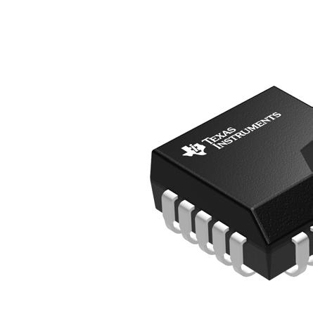
16 GENERIC PACKAGE VIEW DW 16 SOIC mm max height SMALL OUTLINE INTEGRATED CIRCUIT Images above are just a representation of the package family, actual package may vary. Refer to the product data sheet for package details /H
17 SCALE DW0016A PACKAGE OUTLINE SOIC mm max height SOIC C A PIN 1 ID AREA TYP 9.97 SEATING PLANE 0.1 C X NOTE 3 2X B NOTE X C A B 2.65 MAX 0.33 TYP 0.10 SEE DETAIL A 0.25 GAGE PLANE (1.4) DETAIL A TYPICAL /A 07/2016 NOTES: 1. All linear dimensions are in millimeters. Dimensions in parenthesis are for reference only. Dimensioning and tolerancing per ASME Y14.5M. 2. This drawing is subject to change without notice. 3. This dimension does not include mold flash, protrusions, or gate burrs. Mold flash, protrusions, or gate burrs shall not exceed 0.15 mm, per side. 4. This dimension does not include interlead flash. Interlead flash shall not exceed 0.25 mm, per side. 5. Reference JEDEC registration MS
18 DW0016A EXAMPLE BOARD LAYOUT SOIC mm max height SOIC 16X (2) SYMM SEE DETAILS X (0.6) SYMM 14X (1.27) 8 9 R0.05 TYP (9.3) LAND PATTERN EXAMPLE SCALE:7X METAL SOLDER MASK OPENING SOLDER MASK OPENING METAL 0.07 MAX ALL AROUND 0.07 MIN ALL AROUND NON SOLDER MASK DEFINED SOLDER MASK DEFINED SOLDER MASK DETAILS /A 07/2016 NOTES: (continued) 6. Publication IPC-7351 may have alternate designs. 7. Solder mask tolerances between and around signal pads can vary based on board fabrication site.
19 DW0016A EXAMPLE STENCIL DESIGN SOIC mm max height SOIC 16X (2) SYMM X (0.6) SYMM 14X (1.27) 8 9 R0.05 TYP (9.3) SOLDER PASTE EXAMPLE BASED ON mm THICK STENCIL SCALE:7X /A 07/2016 NOTES: (continued) 8. Laser cutting apertures with trapezoidal walls and rounded corners may offer better paste release. IPC-7525 may have alternate design recommendations. 9. Board assembly site may have different recommendations for stencil design.
20
21 IMPORTANT NOTICE Texas Instruments Incorporated (TI) reserves the right to make corrections, enhancements, improvements and other changes to its semiconductor products and services per JESD46, latest issue, and to discontinue any product or service per JESD48, latest issue. Buyers should obtain the latest relevant information before placing orders and should verify that such information is current and complete. TI s published terms of sale for semiconductor products ( apply to the sale of packaged integrated circuit products that TI has qualified and released to market. Additional terms may apply to the use or sale of other types of TI products and services. Reproduction of significant portions of TI information in TI data sheets is permissible only if reproduction is without alteration and is accompanied by all associated warranties, conditions, limitations, and notices. TI is not responsible or liable for such reproduced documentation. Information of third parties may be subject to additional restrictions. Resale of TI products or services with statements different from or beyond the parameters stated by TI for that product or service voids all express and any implied warranties for the associated TI product or service and is an unfair and deceptive business practice. TI is not responsible or liable for any such statements. Buyers and others who are developing systems that incorporate TI products (collectively, Designers ) understand and agree that Designers remain responsible for using their independent analysis, evaluation and judgment in designing their applications and that Designers have full and exclusive responsibility to assure the safety of Designers' applications and compliance of their applications (and of all TI products used in or for Designers applications) with all applicable regulations, laws and other applicable requirements. Designer represents that, with respect to their applications, Designer has all the necessary expertise to create and implement safeguards that (1) anticipate dangerous consequences of failures, (2) monitor failures and their consequences, and (3) lessen the likelihood of failures that might cause harm and take appropriate actions. Designer agrees that prior to using or distributing any applications that include TI products, Designer will thoroughly test such applications and the functionality of such TI products as used in such applications. TI s provision of technical, application or other design advice, quality characterization, reliability data or other services or information, including, but not limited to, reference designs and materials relating to evaluation modules, (collectively, TI Resources ) are intended to assist designers who are developing applications that incorporate TI products; by downloading, accessing or using TI Resources in any way, Designer (individually or, if Designer is acting on behalf of a company, Designer s company) agrees to use any particular TI Resource solely for this purpose and subject to the terms of this Notice. TI s provision of TI Resources does not expand or otherwise alter TI s applicable published warranties or warranty disclaimers for TI products, and no additional obligations or liabilities arise from TI providing such TI Resources. TI reserves the right to make corrections, enhancements, improvements and other changes to its TI Resources. TI has not conducted any testing other than that specifically described in the published documentation for a particular TI Resource. Designer is authorized to use, copy and modify any individual TI Resource only in connection with the development of applications that include the TI product(s) identified in such TI Resource. NO OTHER LICENSE, EXPRESS OR IMPLIED, BY ESTOPPEL OR OTHERWISE TO ANY OTHER TI INTELLECTUAL PROPERTY RIGHT, AND NO LICENSE TO ANY TECHNOLOGY OR INTELLECTUAL PROPERTY RIGHT OF TI OR ANY THIRD PARTY IS GRANTED HEREIN, including but not limited to any patent right, copyright, mask work right, or other intellectual property right relating to any combination, machine, or process in which TI products or services are used. Information regarding or referencing third-party products or services does not constitute a license to use such products or services, or a warranty or endorsement thereof. Use of TI Resources may require a license from a third party under the patents or other intellectual property of the third party, or a license from TI under the patents or other intellectual property of TI. TI RESOURCES ARE PROVIDED AS IS AND WITH ALL FAULTS. TI DISCLAIMS ALL OTHER WARRANTIES OR REPRESENTATIONS, EXPRESS OR IMPLIED, REGARDING RESOURCES OR USE THEREOF, INCLUDING BUT NOT LIMITED TO ACCURACY OR COMPLETENESS, TITLE, ANY EPIDEMIC FAILURE WARRANTY AND ANY IMPLIED WARRANTIES OF MERCHANTABILITY, FITNESS FOR A PARTICULAR PURPOSE, AND NON-INFRINGEMENT OF ANY THIRD PARTY INTELLECTUAL PROPERTY RIGHTS. TI SHALL NOT BE LIABLE FOR AND SHALL NOT DEFEND OR INDEMNIFY DESIGNER AGAINST ANY CLAIM, INCLUDING BUT NOT LIMITED TO ANY INFRINGEMENT CLAIM THAT RELATES TO OR IS BASED ON ANY COMBINATION OF PRODUCTS EVEN IF DESCRIBED IN TI RESOURCES OR OTHERWISE. IN NO EVENT SHALL TI BE LIABLE FOR ANY ACTUAL, DIRECT, SPECIAL, COLLATERAL, INDIRECT, PUNITIVE, INCIDENTAL, CONSEQUENTIAL OR EXEMPLARY DAMAGES IN CONNECTION WITH OR ARISING OUT OF TI RESOURCES OR USE THEREOF, AND REGARDLESS OF WHETHER TI HAS BEEN ADVISED OF THE POSSIBILITY OF SUCH DAMAGES. Unless TI has explicitly designated an individual product as meeting the requirements of a particular industry standard (e.g., ISO/TS and ISO 26262), TI is not responsible for any failure to meet such industry standard requirements. Where TI specifically promotes products as facilitating functional safety or as compliant with industry functional safety standards, such products are intended to help enable customers to design and create their own applications that meet applicable functional safety standards and requirements. Using products in an application does not by itself establish any safety features in the application. Designers must ensure compliance with safety-related requirements and standards applicable to their applications. Designer may not use any TI products in life-critical medical equipment unless authorized officers of the parties have executed a special contract specifically governing such use. Life-critical medical equipment is medical equipment where failure of such equipment would cause serious bodily injury or death (e.g., life support, pacemakers, defibrillators, heart pumps, neurostimulators, and implantables). Such equipment includes, without limitation, all medical devices identified by the U.S. Food and Drug Administration as Class III devices and equivalent classifications outside the U.S. TI may expressly designate certain products as completing a particular qualification (e.g., Q100, Military Grade, or Enhanced Product). Designers agree that it has the necessary expertise to select the product with the appropriate qualification designation for their applications and that proper product selection is at Designers own risk. Designers are solely responsible for compliance with all legal and regulatory requirements in connection with such selection. Designer will fully indemnify TI and its representatives against any damages, costs, losses, and/or liabilities arising out of Designer s noncompliance with the terms and provisions of this Notice. Mailing Address: Texas Instruments, Post Office Box , Dallas, Texas Copyright 2017, Texas Instruments Incorporated
SN54LS670, SN74LS670 4-BY-4 REGISTER FILES WITH 3-STATE OUTPUTS
 SN54LS670, SN74LS670 4-BY-4 REGISTER FILES WITH 3-STATE OUTPUTS SDLS193 MARCH 1974 REVISED MARCH 1988 PRODUCTION DATA information is current as of publication date. Products conform to specifications per
SDLS940A MARCH 1974 REVISED MARCH Copyright 1988, Texas Instruments Incorporated
 SN5490A, SN5492A, SN5493A, SN54LS90, SN54LS92, SN54LS93 SN7490A, SN7492A, SN7493A, SN74LS90, SN74LS92, SN74LS93 DECADE, DIVIDE-BY-TWELVE AND BINARY COUNTERS SDLS940A MARCH 1974 REVISED MARCH 1988 PRODUCTION
SN5446A, 47A, 48, SN54LS47, LS48, LS49 SN7446A, 47A, 48, SN74LS47, LS48, LS49 BCD-TO-SEVEN-SEGMENT DECODERS/DRIVERS
 SN5446A, 47A, 48, SN54LS47, LS48, LS49 SN7446A, 47A, 48, SN74LS47, LS48, LS49 BCD-TO-SEVEN-SEGMENT DECODERS/DRIVERS SDLS111 MARCH 1974 REVISED MARCH 1988 PRODUCTION DATA information is current as of publication
SN54155, SN54156, SN54LS155A, SN54LS156, SN74155, SN74156, SN74LS155A, SN74LS156 DUAL 2-LINE TO 4-LINE DECODERS/DEMULTIPLEXERS
 SN54155, SN54156, SN54LS155A, SN54LS156, SN74155, SN74156, SN74LS155A, SN74LS156 DUAL 2-LINE TO 4-LINE DECODERS/DEMULTIPLEXERS SDLS057 MARCH 1974 REVISED MARCH 1988 PRODUCTION DATA information is current
Data sheet acquired from Harris Semiconductor SCHS287B Revised January 2004
 Data sheet acquired from Harris Semiconductor SCHS287B Revised January 2004 The RCA CD54/74AC240, CD54/74AC241, and CD54/74AC244 and the CD54/74ACT240, CD54/74ACT241, and CD54/74ACT244 3-state octal buffer/line
DUAL SCHOTTKY DIODE BRIDGE
 UC1610 UC3610 DUAL SCHOTTKY DIODE BRIDGE SLUS339B JUNE 1993 REVISED DECEMBER 2004 FEATURES Monolithic Eight-Diode Array Exceptional Efficiency Low Forward Voltage Fast Recovery Time High Peak Current Small
Data sheet acquired from Harris Semiconductor SCHS098D Revised October 2003
 Data sheet acquired from Harris Semiconductor SCHS098D Revised October 2003 The CD40107B is a dual 2-input NAND buffer/driver containing two independent 2-input NAND buffers with open-drain single n-channel
SN5446A, 47A, 48, SN54LS47, LS48, LS49 SN7446A, 47A, 48, SN74LS47, LS48, LS49 BCD-TO-SEVEN-SEGMENT DECODERS/DRIVERS
 SN5446A, 47A, 48, SN54LS47, LS48, LS49 SN7446A, 47A, 48, SN74LS47, LS48, LS49 BCD-TO-SEVEN-SEGMENT DECODERS/DRIVERS SDLS111 MARCH 1974 REVISED MARCH 1988 PRODUCTION DATA information is current as of publication
The CD54AC540, -541, and CD54ACT540, -541, available in chip form (H suffix), are operable over the 55 to +125 C temperature range.
, are operable over the 55 to +125 C temperature range.") Data sheet acquired from Harris Semiconductor SCHS285A Revised November 1999 The CD54/74AC540, -541, and CD54/74ACT540, -541 octal buffer/line drivers use the RCA ADVANCED CMOS technology. The CD54/74AC/ACT540
Data sheet acquired from Harris Semiconductor SCHS285A Revised November 1999 The CD54/74AC540, -541, and CD54/74ACT540, -541 octal buffer/line drivers use the RCA ADVANCED CMOS technology. The CD54/74AC/ACT540
SN5446A, 47A, 48, SN54LS47, LS48, LS49 SN7446A, 47A, 48, SN74LS47, LS48, LS49 BCD-TO-SEVEN-SEGMENT DECODERS/DRIVERS
 SN5446A, 47A, 48, SN54LS47, LS48, LS49 SN7446A, 47A, 48, SN74LS47, LS48, LS49 BCD-TO-SEVEN-SEGMENT DECODERS/DRIVERS SDLS111 MARCH 1974 REVISED MARCH 1988 PRODUCTION DATA information is current as of publication
Data sheet acquired from Harris Semiconductor SCHS091B Revised July 2003
 Data sheet acquired from Harris Semiconductor SCHS091B Revised July 2003 The CD4585B types are supplied in 16-lead hermetic dual-in-line ceramic packages (F3A suffix), 16-lead dual-in-line plastic packages
SN54390, SN54LS390, SN54393, SN54LS393 SN74390, SN74LS390, SN74393, SN74LS393 DUAL 4-BIT DECADE AND BINARY COUNTERS
 SN54390, SN54LS390, SN54393, SN54LS393 SN74390, SN74LS390, SN74393, SN74LS393 DUAL 4-BIT DECADE AND BINARY COUNTERS SDLS107 OCTOBER 1976 REVISED MARCH 1988 PRODUCTION DATA information is current as of
SDLS940A MARCH 1974 REVISED MARCH Copyright 1988, Texas Instruments Incorporated
 SN5490A, SN5492A, SN5493A, SN54LS90, SN54LS92, SN54LS93 SN7490A, SN7492A, SN7493A, SN74LS90, SN74LS92, SN74LS93 DECADE, DIVIDE-BY-TWELVE AND BINARY COUNTERS SDLS940A MARCH 1974 REVISED MARCH 1988 PRODUCTION
For data sheet and general inquiries on the UCD30xx part family, please contact
 For data sheet and general inquiries on the UCD30xx part family, please contact ucd30xxdigitalpowersupport@list.ti.com PACKAGE MATERIALS INFORMATION www.ti.com 14-Jul-2012 TAPE AND REEL INFORMATION *All
Data sheet acquired from Harris Semiconductor SCHS058C Revised October 2003
 Data sheet acquired from Harris Semiconductor SCHS058C Revised October 2003 The CD4076B types are supplied in 16-lead hermetic dual-in-line ceramic packages (F3A suffix), 16-lead dual-in-line plastic packages
SN54LS292, SN54LS294, SN74LS292, SN74LS294 PROGRAMMABLE FREQUENCY DIVIDERS/DIGITAL TIMERS
 PRODUCTION DATA information is current as of publication date. Products conform to specifications per the terms of Texas Instruments standard warranty. Production processing does not necessarily include
 Distributed by: www.jameco.com 1-800-831-4242 The content and copyrights of the attached material are the property of its owner. Data sheet acquired from Harris Semiconductor SCHS086D Revised April 2004
Data sheet acquired from Harris Semiconductor SCHS018C Revised September 2003
 Data sheet acquired from Harris Semiconductor SCHS018C Revised September 2003 The CD4007UB types are supplied in 14-lead hermetic dual-in-line ceramic packages (F3A suffix), 14-lead dual-in-line plastic
SN5473, SN54LS73A, SN7473, SN74LS73A DUAL J-K FLIP-FLOPS WITH CLEAR
 SN5473, SN54LS73A, SN7473, SN74LS73A DUAL J-K FLIP-FLOPS WITH CLEAR SDLS118 DECEMBER 1983 REVISED MARCH 1988 PRODUCTION DATA information is current as of publication date. Products conform to specifications
Data sheet acquired from Harris Semiconductor SCHS015C Revised August 2003
 Data sheet acquired from Harris Semiconductor SCHS015C Revised August 2003 The CD4001B, CD4002B, and CD4025B types are supplied in 14-lead hermetic dual-in-line ceramic packages (F3A suffix), 14-lead dual-in-line
SDLS940A MARCH 1974 REVISED MARCH Copyright 1988, Texas Instruments Incorporated
 SN5490A, SN5492A, SN5493A, SN54LS90, SN54LS92, SN54LS93 SN7490A, SN7492A, SN7493A, SN74LS90, SN74LS92, SN74LS93 DECADE, DIVIDE-BY-TWELVE AND BINARY COUNTERS SDLS940A MARCH 1974 REVISED MARCH 1988 PRODUCTION
 Distributed by: www.jameco.com 1-800-831-4242 The content and copyrights of the attached material are the property of its owner. Data sheet acquired from Harris Semiconductor SCHS057C Revised September
SDLS940A MARCH 1974 REVISED MARCH Copyright 1988, Texas Instruments Incorporated
 SN5490A, SN5492A, SN5493A, SN54LS90, SN54LS92, SN54LS93 SN7490A, SN7492A, SN7493A, SN74LS90, SN74LS92, SN74LS93 DECADE, DIVIDE-BY-TWELVE AND BINARY COUNTERS SDLS940A MARCH 1974 REVISED MARCH 1988 PRODUCTION
 Distributed by: www.jameco.com 1-800-831-4242 The content and copyrights of the attached material are the property of its owner. Data sheet acquired from Harris Semiconductor SCHS072B Revised July 2003
 Distributed by: www.jameco.com 1-800-831-4242 The content and copyrights of the attached material are the property of its owner. Data sheet acquired from Harris Semiconductor SCHS021D Revised September
SN5495A, SN54LS95B SN7495A, SN74LS95B 4-BIT PARALLEL-ACCESS SHIFT REGISTERS
 PRODUCTION DATA information is current as of publication date. Products conform to specifications per the terms of Texas Instruments standard warranty. Production processing does not necessarily include
SDLS940A MARCH 1974 REVISED MARCH Copyright 1988, Texas Instruments Incorporated
 PRODUCTION DATA information is current as of publication date. Products conform to specifications per the terms of Texas Instruments standard warranty. Production processing does not necessarily include
SN54LS181, SN54S181 SN74LS181, SN74S181 ARITHMETIC LOGIC UNITS/FUNCTION GENERATORS
 PRODUCTION DATA information is current as of publication date. Products conform to specifications per the terms of Texas Instruments standard warranty. Production processing does not necessarily include
SDLS047 DECEMBER 1983 REVISED MARCH 1988
 SDLS047 DECEMBER 1983 REVISED MARCH 1988 Copyright 1988, Texas Instruments Incorporated POST OFFICE BOX 655303 DALLAS, TEXAS 75265 1 SDLS047 DECEMBER 1983 REVISED MARCH 1988 2 POST OFFICE BOX 655303 DALLAS,
SN5473, SN54LS73A, SN7473, SN74LS73A DUAL J-K FLIP-FLOPS WITH CLEAR
 SN5473, SN54LS73A, SN7473, SN74LS73A DUAL J-K FLIP-FLOPS WITH CLEAR SDLS118 DECEMBER 1983 REVISED MARCH 1988 PRODUCTION DATA information is current as of publication date. Products conform to specifications
SN5473, SN54LS73A, SN7473, SN74LS73A DUAL J-K FLIP-FLOPS WITH CLEAR
 SN5473, SN54LS73A, SN7473, SN74LS73A DUAL J-K FLIP-FLOPS WITH CLEAR SDLS118 DECEMBER 1983 REVISED MARCH 1988 PRODUCTION DATA information is current as of publication date. Products conform to specifications
SN54S140, SN74S140 DUAL 4-INPUT POSITIVE-NAND 50-OHM LINE DRIVERS
 SN54S140, SN74S140 DUAL 4-INPUT POSITIVE-NAND 50-OHM LINE DRIVERS SDLS210 DECEMBER 1983 REVISED MARCH 1988 PRODUCTION Products conform DATA to specifications information is per current the terms as of
SDLS940A MARCH 1974 REVISED MARCH Copyright 1988, Texas Instruments Incorporated
 PRODUCTION DATA information is current as of publication date. Products conform to specifications per the terms of Texas Instruments standard warranty. Production processing does not necessarily include
Figure 1 Input power cable (left) and output power cable (right)
 and output power cable (right)") TIDA-00282 Cable Assemblies These cable assemblies are intended for use with the C2000-based Automotive Digitally-controlled Boost Power Supply board described in TI Designs TIDA-00282. Figure 1 Input
TIDA-00282 Cable Assemblies These cable assemblies are intended for use with the C2000-based Automotive Digitally-controlled Boost Power Supply board described in TI Designs TIDA-00282. Figure 1 Input
SN5410, SN54LS10, SN54S10, SN7410, SN74LS10, SN74S10 TRIPLE 3-INPUT POSITIVE-NAND GATES
 SN540, SN54LS0, SN54S0, SN740, SN74LS0, SN74S0 TRIPLE 3-INPUT POSITIVE-NAND GATES SDLS035A DECEMBER 983 REVISED APRIL 2003 PRODUCTION DATA information is current as of publication date. Products conform
SN5446A, 47A, 48, SN54LS47, LS48, LS49 SN7446A, 47A, 48, SN74LS47, LS48, LS49 BCD-TO-SEVEN-SEGMENT DECODERS/DRIVERS
 PRODUCTION DATA information is current as of publication date. Products conform to specifications per the terms of Texas Instruments standard warranty. Production processing does not necessarily include
SDLS068A DECEMBER 1972 REVISED OCTOBER Copyright 2001, Texas Instruments Incorporated
 SN54174, SN54175, SN54LS174, SN54LS175, SN54S174, SN54S175, SN74174, SN74175, SN74LS174, SN74LS175, SN74S174, SN74S175 PRODUCTION DATA information is current as of publication date. Products conform to
 Distributed by: www.jameco.com 1-800-831-4242 The content and copyrights of the attached material are the property of its owner. Data sheet acquired from Harris Semiconductor SCHS044A Revised March 2002
Guidelines for Returns (SPRAC01A SEPTEMBER 2017)
") Guidelines for Returns (SPRAC01A SEPTEMBER 2017) Introduction Texas Instruments (TI) strives to provide quality products and is continuously improving products, processes and services. To enable an efficient
Guidelines for Returns (SPRAC01A SEPTEMBER 2017) Introduction Texas Instruments (TI) strives to provide quality products and is continuously improving products, processes and services. To enable an efficient
SN65HVD257D CAN EVM. CAN Transceivers with Fast Loop Times for Highly Loaded Networks and Features For Functional Safety Networks REVISION: A
 EVM TEST PROCEDURE SN65HVD257D CAN EVM CAN Transceivers with Fast Loop Times for Highly Loaded Networks and Features For Functional Safety Networks REVISION: A By: Scott Monroe and Jason Blackman REVISION
Package Mounting Guide SOP/QFP
 Package Mounting Guide Revision 1.0 2016-03 2016-03-17 1 / 14 Rev. 1.0 2016 Toshiba Corporation Table of Contents Package Mounting Guide Preface... 4 Purpose of this document... 4 Intended Audience...
Section 7. Additional Information on Products, Tools and Support
 Section 7 Additional Information on Products, Tools and Support From 7-1 For more information on Data Converters please look at the Texas Instruments data converter home page: This page provides access
CD4071B Quad 2-Input OR Gate CD4072B Dual 4-Input OR Gate CD4075B Triple 3-Input OR Gate
 Data sheet acquired from Harris Semiconductor SCHS056D Revised August 2003 CD4071B Quad 2-Input OR Gate CD4072B Dual 4-Input OR Gate CD4075B Triple 3-Input OR Gate CD4071B, CD4072B, and CD4075B OR gates
AN Recommendations for PCB assembly of DSN1006. Document information
 Recoendations for PCB assembly of DSN1006 Rev. 1 29 July 2015 Application note Document information Info Keywords Abstract Content DSN1006, DSN1006-2, DSN1006U-2, SOD993, SOD995, 0402 package size, reflow
AN Recommendations for PCB assembly of DSN Document information
 Rev. 2 23 September 2015 Application note Document information Info Keywords Abstract Content DSN0603, DSN0603-2, SOD962, 0603 package size, reflow soldering, surface mount, solder paste, stencil aperture,
TC4W53F/FU
 1 2 3 4 5 RESTRICTIONS ON PRODUCT USE Toshiba Corporation, and its subsidiaries and affiliates (collectively TOSHIBA ), reserve the right to make changes to the information in this document, and related
Package Mounting Guide BGA
 Package Mounting Guide Revision 1.0 2017-03 2017-03-17 1 / 16 Rev. 1.0 2017 Toshiba Corporation Table of Contents Package Mounting Guide Preface... 4 Purpose of this document... 4 Intended Audience...
Platform Flash PROM VOG48 Package Lead Finish Conversion to NiPdAu
 Platform Flash PROM VOG48 Package Lead Finish Conversion to NiPdAu Qualification Report Xilinx is disclosing this Qualification Report (the Documentation ) to you solely for use in the development of designs
Reliability Tests Report
 Product Name: Package Name: CRS12 SFLAT Reliability Tests Report 1. Thermal tests Peak : 260 deg.c(a moment) Reflow zone : 230 deg.c 30 to 50 s Preheat : 180 to 190 deg.c, 60 to 120 s 3 times Peak : 260
SMV LF: Hyperabrupt Junction Tuning Varactor
 DATA SHEET SMV1145-079LF: Hyperabrupt Junction Tuning Varactor Applications High volume commercial systems Features Frequency linear design Low series resistance Package is rated MSL1, 260 C per JEDEC
1SS427 1SS Applications. 2. Packaging and Internal Circuit Rev.3.0. Start of commercial production
 Switching Diodes 1SS427 Silicon Epitaxial Planar 1SS427 1. Applications Ultra-High-Speed Switching 2. Packaging and Internal Circuit 1: Cathode 2: Anode SOD-923 1: Cathode 2: Anode fsc 1 Start of commercial
Recommended Land Pattern: [mm] Stencil Suggestion:
![Recommended Land Pattern: [mm] Stencil Suggestion:](/thumbs/77/75627151.jpg "Recommended Land Pattern: [mm] Stencil Suggestion:") Dimensions: [mm] Recommended Land Pattern: [mm] Properties: Properties Value Unit Thread M3 Inner Diameter Ø ID 4.2 mm O 6,0 G u 0,1 1,0 O 4,2 sectional drawing - M 3,0 Suggested Solder pad Non plated
Dimensions: [mm] Recommended Land Pattern: [mm] Properties: Properties Value Unit Thread M3 Inner Diameter Ø ID 4.2 mm O 6,0 G u 0,1 1,0 O 4,2 sectional drawing - M 3,0 Suggested Solder pad Non plated
Recommended Land Pattern: [mm] Stencil Suggestion:
![Recommended Land Pattern: [mm] Stencil Suggestion:](/thumbs/90/103462493.jpg "Recommended Land Pattern: [mm] Stencil Suggestion:") Dimensions: [mm] Recommended Land Pattern: [mm] Properties: Properties Value Unit Thread M3 Inner Diameter Ø ID 4.2 mm O 6,0 G u 0,1 1,0 O 4,2 sectional drawing - M 3,0 Suggested Solder pad Non plated
Dimensions: [mm] Recommended Land Pattern: [mm] Properties: Properties Value Unit Thread M3 Inner Diameter Ø ID 4.2 mm O 6,0 G u 0,1 1,0 O 4,2 sectional drawing - M 3,0 Suggested Solder pad Non plated
Recommended Land Pattern: [mm]
![Recommended Land Pattern: [mm]](/thumbs/91/105181600.jpg "Recommended Land Pattern: [mm]") Dimensions: [mm] Recommended Land Pattern: [mm] Electrical Properties: Properties Test conditions Value Unit Tol. Frequency Range f 5150-5875 MHz 1,3 Insertion Loss IL 5150-5875 MHz 1.5 db max. VSWR 5150-5875
Dimensions: [mm] Recommended Land Pattern: [mm] Electrical Properties: Properties Test conditions Value Unit Tol. Frequency Range f 5150-5875 MHz 1,3 Insertion Loss IL 5150-5875 MHz 1.5 db max. VSWR 5150-5875
CFN Series Metal Foil, Current Sense Resistor
 RoHS COMPLIANT* & HALOGEN FREE** Features n Metal foil n High power density n High reliability and stability n RoHS compliant* and halogen free** Applications n Current sensing n Power supplies n Stepper
General Information on the Assembly and Solder Pad Design of the DRAGON Family Application Note
 General Information on the Assembly and Solder Pad Design of the DRAGON Family Application Note Abstract This application note gives general information on the assembly and design of the solder pad of
Package LGA6x FixPitch- / FreePitch-Sensors
 Package LG6x FixPitch- / FreePitch-Sensors LG6x.HIE.03 Page 1 of 6 1. Packaging Package LG6x The sensors are delivered in vacuum sealed, ESD-compliant dry bag. The series delivery form is tape & reel with
Phase Shifter. No. SP-LFZ P1/6. 1. Electrical Characteristics (at -40 ~ +85 C) Nominal Characteristics Impedance
 Nominal Characteristics Impedance") P1/6 Phase Shifter 1. Electrical Characteristics (at -40 ~ +85 C) LFP152G5E090F123TEMP 0.48 db max. at +25 C 0. 53 db max. at -40 ~ +85 C 13.0 db min. at 200.00 ~ 400.00 MHz 94.5 ± 5.5 at 2400.00 MHz 90.0
P1/6 Phase Shifter 1. Electrical Characteristics (at -40 ~ +85 C) LFP152G5E090F123TEMP 0.48 db max. at +25 C 0. 53 db max. at -40 ~ +85 C 13.0 db min. at 200.00 ~ 400.00 MHz 94.5 ± 5.5 at 2400.00 MHz 90.0
Recommended Land Pattern: [mm]
![Recommended Land Pattern: [mm]](/thumbs/92/108685678.jpg "Recommended Land Pattern: [mm]") Dimensions: [mm] Recommended Land Pattern: [mm] Electrical Properties: Properties Test conditions Value Unit Tol. Inductance L 1.06 MHz 22 µh ±10% Rated Current I R ΔT = 40 K 650 ma max. DC Resistance
Dimensions: [mm] Recommended Land Pattern: [mm] Electrical Properties: Properties Test conditions Value Unit Tol. Inductance L 1.06 MHz 22 µh ±10% Rated Current I R ΔT = 40 K 650 ma max. DC Resistance
High Temperature (245 C) Thick Film Chip Resistor
 Thick Film Chip Resistor") High Temperature (245 C) Thick Film Chip Resistor For applications such as down hole applications or aircraft breaking systems, the need for parts able to withstand very severe conditions (temperature
High Temperature (245 C) Thick Film Chip Resistor For applications such as down hole applications or aircraft breaking systems, the need for parts able to withstand very severe conditions (temperature
Recommended Land Pattern: [mm] Stencil Suggestion:
![Recommended Land Pattern: [mm] Stencil Suggestion:](/thumbs/82/86769336.jpg "Recommended Land Pattern: [mm] Stencil Suggestion:") Dimensions: [mm] Recommended Land Pattern: [mm] Properties: 6:1 detail B O3,2 Solder Pad Properties Value Unit Material Brass Surface Tin ±0,1 ±0,1 Bevelled edge 0,5 ±0,1 around 3,0 ±0,2 O1,85 Via Tightening
Dimensions: [mm] Recommended Land Pattern: [mm] Properties: 6:1 detail B O3,2 Solder Pad Properties Value Unit Material Brass Surface Tin ±0,1 ±0,1 Bevelled edge 0,5 ±0,1 around 3,0 ±0,2 O1,85 Via Tightening
Recommended Land Pattern: [mm]
![Recommended Land Pattern: [mm]](/thumbs/77/75871344.jpg "Recommended Land Pattern: [mm]") Dimensions: [mm] 0,3 ± 0,1 Recommended Land Pattern: [mm] 0,762 Electrical Properties: Properties Test conditions Value Unit Tol. Inductance 200 MHz L 56 nh ±5% Q-Factor 200 MHz Q min. 32 min. DC Resistance
Dimensions: [mm] 0,3 ± 0,1 Recommended Land Pattern: [mm] 0,762 Electrical Properties: Properties Test conditions Value Unit Tol. Inductance 200 MHz L 56 nh ±5% Q-Factor 200 MHz Q min. 32 min. DC Resistance
Recommended Land Pattern: [mm]
![Recommended Land Pattern: [mm]](/thumbs/94/118765902.jpg "Recommended Land Pattern: [mm]") Dimensions: [mm] 0,3 ± 0,1 Recommended Land Pattern: [mm] 0,762 Electrical Properties: Properties Test conditions Value Unit Tol. Inductance 250 MHz L 11 nh ±5% Q-Factor 250 MHz Q min. 30 min. DC Resistance
Dimensions: [mm] 0,3 ± 0,1 Recommended Land Pattern: [mm] 0,762 Electrical Properties: Properties Test conditions Value Unit Tol. Inductance 250 MHz L 11 nh ±5% Q-Factor 250 MHz Q min. 30 min. DC Resistance
Low Maintenance AC Powered Security Gate
 AN-9002 IPC Application Note: Low Maintenance AC Powered Security Gate Mechanical Gate components: A typical Security Gate system consists of the gate, a rail or guide system, one or two motors, a cable
Recommended Land Pattern: [mm] Stencil Suggestion:
![Recommended Land Pattern: [mm] Stencil Suggestion:](/thumbs/90/102451029.jpg "Recommended Land Pattern: [mm] Stencil Suggestion:") Dimensions: [mm] Recommended Land Pattern: [mm] Properties: Properties Value Unit ±0,1 Bevelled edge 0,5 ±0,1 around 5:1 detail B 3,0 ±0,2 O3,2 Solder Pad non plated through-hole Material Brass Surface
Dimensions: [mm] Recommended Land Pattern: [mm] Properties: Properties Value Unit ±0,1 Bevelled edge 0,5 ±0,1 around 5:1 detail B 3,0 ±0,2 O3,2 Solder Pad non plated through-hole Material Brass Surface
TMS320C6000 BGA Manufacturing Considerations
 TMS320C6000 BGA Manufacturing Considerations David Bell C6000 Applications Team Abstract When designing with a high-density BGA package, it is important to be aware of different techniques that aid in
CRK Series Metal Strip, Wide Terminal Current Sense Resistor
 RoHS COMPLIANT* & HALOGEN FREE** Features n ide terminal type n Excellent heat dissipation n High reliability n Metal alloy plate n RoHS compliant* and halogen free** Applications n Current sensing n Power
TMS320C6x Manufacturing with the BGA Package
 TMS320C6x Manufacturing with the BGA Package APPLICATION REPORT: SPRA429 David Bell Digital Signal Processing Solutions March 1998 IMPORTANT NOTICE Texas Instruments (TI) reserves the right to make changes
PHASE SHIFTER. No. LFP15CE-01 P1/ Electrical Characteristics (at -40 ~ +85 C) Nominal Characteristics Impedance
 Nominal Characteristics Impedance") No. LFP15CE-01 P1/12 PHASE SHIFTER 1. Electrical Characteristics (at -40 ~ +85 C) LFP151G9E030E111 0.70 db max. at +25 C 0. 80 db max. at -40 ~ +85 C 0.50 db max. at +25 C 0.60 db max. at -40 ~ +85 C 0.50
No. LFP15CE-01 P1/12 PHASE SHIFTER 1. Electrical Characteristics (at -40 ~ +85 C) LFP151G9E030E111 0.70 db max. at +25 C 0. 80 db max. at -40 ~ +85 C 0.50 db max. at +25 C 0.60 db max. at -40 ~ +85 C 0.50
Recommended Land Pattern: [mm]
![Recommended Land Pattern: [mm]](/thumbs/92/108683517.jpg "Recommended Land Pattern: [mm]") Dimensions: [mm] 2,5 ±0,2 Recommended Land Pattern: [mm] 2,7 Electrical Properties: Properties Test conditions Value Unit Tol. Inductance L 100 khz/ 1 V 2.2 µh ±20% Rated Current I R ΔT = 40 K 1.8 A max.
Dimensions: [mm] 2,5 ±0,2 Recommended Land Pattern: [mm] 2,7 Electrical Properties: Properties Test conditions Value Unit Tol. Inductance L 100 khz/ 1 V 2.2 µh ±20% Rated Current I R ΔT = 40 K 1.8 A max.
Product Marking: Schematic: General Properties: WE-PD SMT Shielded Power Inductor SIZE REVISION STATUS DATE (YYYY-MM-DD) BUSINESS UNIT PAGE
 BUSINESS UNIT PAGE") Product Marking: Start of Winding Schematic: General Properties: It is recommended that the temperature of the component does not exceed +125 C under worst case conditions Storage Conditions (in original
Product Marking: Start of Winding Schematic: General Properties: It is recommended that the temperature of the component does not exceed +125 C under worst case conditions Storage Conditions (in original
Recommended Land Pattern: [mm]
![Recommended Land Pattern: [mm]](/thumbs/92/108389450.jpg "Recommended Land Pattern: [mm]") Dimensions: [mm] 8,0 ±0,3 5,0 ±0,2 12,0 ±0,5 10,0 max. Recommended Land Pattern: [mm] 5,4 7,0 2,9 12,8 no vias and sensitive traces underneath the component Scale - 2:1 Schematic: Electrical Properties:
Dimensions: [mm] 8,0 ±0,3 5,0 ±0,2 12,0 ±0,5 10,0 max. Recommended Land Pattern: [mm] 5,4 7,0 2,9 12,8 no vias and sensitive traces underneath the component Scale - 2:1 Schematic: Electrical Properties:
Recommended Land Pattern: [mm]
![Recommended Land Pattern: [mm]](/thumbs/92/109322159.jpg "Recommended Land Pattern: [mm]") Dimensions: [mm] 8,0 ±0,3 5,0 ±0,2 12,0 ±0,5 10,0 max. Recommended Land Pattern: [mm] 5,4 7,0 2,9 12,8 no vias and sensitive traces underneath the component Scale - 2:1 Schematic: Electrical Properties:
Dimensions: [mm] 8,0 ±0,3 5,0 ±0,2 12,0 ±0,5 10,0 max. Recommended Land Pattern: [mm] 5,4 7,0 2,9 12,8 no vias and sensitive traces underneath the component Scale - 2:1 Schematic: Electrical Properties:
Recommended Land Pattern: [mm]
![Recommended Land Pattern: [mm]](/thumbs/74/69946433.jpg "Recommended Land Pattern: [mm]") Dimensions: [mm] Recommended Land Pattern: [mm] Electrical Properties: Properties Test conditions Value Unit Tol. 1,7 Inductance 100 khz/ 250 mv L 47 µh ±20% Rated Current ΔT = 40 K I R 1.1 A max. 4,0
Dimensions: [mm] Recommended Land Pattern: [mm] Electrical Properties: Properties Test conditions Value Unit Tol. 1,7 Inductance 100 khz/ 250 mv L 47 µh ±20% Rated Current ΔT = 40 K I R 1.1 A max. 4,0
Recommended Land Pattern: [mm]
![Recommended Land Pattern: [mm]](/thumbs/93/112534808.jpg "Recommended Land Pattern: [mm]") Dimensions: [mm] 8,0 ±0,3 5,0 ±0,2 12,0 ±0,5 Recommended Land Pattern: [mm] 5,4 7,0 2,9 12,8 no vias and sensitive traces underneath the component Scale - 2:1 Schematic: Electrical Properties: Properties
Dimensions: [mm] 8,0 ±0,3 5,0 ±0,2 12,0 ±0,5 Recommended Land Pattern: [mm] 5,4 7,0 2,9 12,8 no vias and sensitive traces underneath the component Scale - 2:1 Schematic: Electrical Properties: Properties
Recommended Land Pattern: [mm]
![Recommended Land Pattern: [mm]](/thumbs/93/113495291.jpg "Recommended Land Pattern: [mm]") Dimensions: [mm] 8,0 ±0,3 5,0 ±0,2 12,0 ±0,5 10,0 max. Recommended Land Pattern: [mm] 5,4 7,0 2,9 12,8 no vias and sensitive traces underneath the component Scale - 2:1 Schematic: Electrical Properties:
Dimensions: [mm] 8,0 ±0,3 5,0 ±0,2 12,0 ±0,5 10,0 max. Recommended Land Pattern: [mm] 5,4 7,0 2,9 12,8 no vias and sensitive traces underneath the component Scale - 2:1 Schematic: Electrical Properties:
Recommended Land Pattern: [mm]
![Recommended Land Pattern: [mm]](/thumbs/93/113836283.jpg "Recommended Land Pattern: [mm]") Dimensions: [mm] 8,0 ±0,3 5,0 ±0,2 12,0 ±0,5 10,0 max. Recommended Land Pattern: [mm] 5,4 7,0 2,9 12,8 no vias and sensitive traces underneath the component Scale - 2:1 Schematic: Electrical Properties:
Dimensions: [mm] 8,0 ±0,3 5,0 ±0,2 12,0 ±0,5 10,0 max. Recommended Land Pattern: [mm] 5,4 7,0 2,9 12,8 no vias and sensitive traces underneath the component Scale - 2:1 Schematic: Electrical Properties:
Recommended Land Pattern: [mm]
![Recommended Land Pattern: [mm]](/thumbs/94/119206143.jpg "Recommended Land Pattern: [mm]") Dimensions: [mm] Recommended Land Pattern: [mm] Electrical & Optical Properties: Properties Test conditions Value Unit Tol. 2,05 6,05 2,05 Inductance L 100 khz/ 10 ma 1.8 µh ±20% Rated Current I R ΔT =
Dimensions: [mm] Recommended Land Pattern: [mm] Electrical & Optical Properties: Properties Test conditions Value Unit Tol. 2,05 6,05 2,05 Inductance L 100 khz/ 10 ma 1.8 µh ±20% Rated Current I R ΔT =
Recommended Land Pattern: [mm]
![Recommended Land Pattern: [mm]](/thumbs/92/108683501.jpg "Recommended Land Pattern: [mm]") Dimensions: [mm] Recommended Land Pattern: [mm] Electrical Properties: Properties Test conditions Value Unit Tol. 1,7 Inductance L 1 khz/ 250 mv 47 µh ±20% Rated Current I R ΔT = 40 K 1.03 A max. 1,5 ±0,3
Dimensions: [mm] Recommended Land Pattern: [mm] Electrical Properties: Properties Test conditions Value Unit Tol. 1,7 Inductance L 1 khz/ 250 mv 47 µh ±20% Rated Current I R ΔT = 40 K 1.03 A max. 1,5 ±0,3
Recommended Land Pattern: [mm]
![Recommended Land Pattern: [mm]](/thumbs/96/126600407.jpg "Recommended Land Pattern: [mm]") Dimensions: [mm] 8,0 ±0,3 5,0 ±0,2 12,0 ±0,5 Recommended Land Pattern: [mm] 5,4 7,0 2,9 12,8 no vias and sensitive traces underneath the component Scale - 2:1 Schematic: Electrical Properties: Properties
Dimensions: [mm] 8,0 ±0,3 5,0 ±0,2 12,0 ±0,5 Recommended Land Pattern: [mm] 5,4 7,0 2,9 12,8 no vias and sensitive traces underneath the component Scale - 2:1 Schematic: Electrical Properties: Properties
Recommended Land Pattern: [mm]
![Recommended Land Pattern: [mm]](/thumbs/93/112799635.jpg "Recommended Land Pattern: [mm]") Dimensions: [mm] Recommended Land Pattern: [mm] Electrical Properties: Properties Test conditions Value Unit Tol. 1,7 Inductance L 1 khz/ 250 mv 10 µh ±20% Rated Current I R ΔT = 40 K 1.83 A max. 1,5 ±0,3
Dimensions: [mm] Recommended Land Pattern: [mm] Electrical Properties: Properties Test conditions Value Unit Tol. 1,7 Inductance L 1 khz/ 250 mv 10 µh ±20% Rated Current I R ΔT = 40 K 1.83 A max. 1,5 ±0,3
DRAFT. Recommended Land Pattern: [mm] Electrical Properties: Dimensions: [mm] Schematic: General Properties: Product Marking:
![DRAFT. Recommended Land Pattern: [mm] Electrical Properties: Dimensions: [mm] Schematic: General Properties: Product Marking:](/thumbs/91/106053527.jpg "DRAFT. Recommended Land Pattern: [mm] Electrical Properties: Dimensions: [mm] Schematic: General Properties: Product Marking:") Dimensions: [mm] Recommended Land Pattern: [mm] Electrical Properties: Properties Test conditions Value Unit Tol. Inductance L 100 khz/ 1 ma 2.2 µh ±20% Start of Winding Marking 4,8 ±0,3 Product Marking:
Dimensions: [mm] Recommended Land Pattern: [mm] Electrical Properties: Properties Test conditions Value Unit Tol. Inductance L 100 khz/ 1 ma 2.2 µh ±20% Start of Winding Marking 4,8 ±0,3 Product Marking:
TOSHIBA Transistor Silicon PNP Epitaxial Type (PCT Process) (Bias Resistor built-in Transistor) RN2110, RN2111
 (Bias Resistor built-in Transistor) RN2110, RN2111") , TOSHIBA Transistor Silicon PNP Epitaxial Type (PCT Process) (Bias Resistor built-in Transistor), Switching, Inverter Circuit, Interface Circuit and Driver Circuit Applications Built-in bias resistors
, TOSHIBA Transistor Silicon PNP Epitaxial Type (PCT Process) (Bias Resistor built-in Transistor), Switching, Inverter Circuit, Interface Circuit and Driver Circuit Applications Built-in bias resistors
PCB Mount VIA Soldering Guidelines
 APPLICATION NOTE AN:401 PCB Mount VIA Soldering Guidelines Ankur Patel Applications Engineering Contents Page Introduction 1 Storage 1 Handling 1 Placement 1 Soldering Process 2 Fluxing 2 Preheating 3
Recommended Land Pattern: [mm]
![Recommended Land Pattern: [mm]](/thumbs/95/124859995.jpg "Recommended Land Pattern: [mm]") Dimensions: [mm] Recommended Land Pattern: [mm] Electrical Properties: Properties Test conditions Value Unit Tol. 5,0 Inductance L 100 khz/ 100 mv 4.7 µh ±20% Rated Inductance L R 100 khz/ 100 mv/ 13.0
Dimensions: [mm] Recommended Land Pattern: [mm] Electrical Properties: Properties Test conditions Value Unit Tol. 5,0 Inductance L 100 khz/ 100 mv 4.7 µh ±20% Rated Inductance L R 100 khz/ 100 mv/ 13.0
A Component Supplier s Green Approach Texas Instruments
 A Component Supplier s Green Approach Texas Instruments IPC/JEDEC Pb-free Conference Dallas, TX Dec 9, 2008 Mark Frimann 1 Texas Instruments & RoHS Nickel-Palladium-Gold RoHS Compliant Solutions (no Tin
Recommended Land Pattern: [mm]
![Recommended Land Pattern: [mm]](/thumbs/92/109149930.jpg "Recommended Land Pattern: [mm]") Dimensions: [mm] Recommended Land Pattern: [mm] Electrical Properties: Properties Test conditions Value Unit Tol. RDC is measured at these points. Inductance L 100 khz/ 10 ma 4.7 µh ±20% Rated Current
Dimensions: [mm] Recommended Land Pattern: [mm] Electrical Properties: Properties Test conditions Value Unit Tol. RDC is measured at these points. Inductance L 100 khz/ 10 ma 4.7 µh ±20% Rated Current
Recommended Land Pattern: [mm]
![Recommended Land Pattern: [mm]](/thumbs/92/109215094.jpg "Recommended Land Pattern: [mm]") Dimensions: [mm] Recommended Land Pattern: [mm] Electrical Properties: Properties Test conditions Value Unit Tol. RDC is measured at these points. Inductance L 100 khz/ 10 ma 2.2 µh ±20% Rated Current
Dimensions: [mm] Recommended Land Pattern: [mm] Electrical Properties: Properties Test conditions Value Unit Tol. RDC is measured at these points. Inductance L 100 khz/ 10 ma 2.2 µh ±20% Rated Current
Recommended Land Pattern: [mm]
![Recommended Land Pattern: [mm]](/thumbs/95/124810191.jpg "Recommended Land Pattern: [mm]") Dimensions: [mm] Recommended Land Pattern: [mm] Electrical Properties: Properties Test conditions Value Unit Tol. RDC is measured at these points. Inductance L 100 khz/ 10 ma 0.68 µh ±20% Rated Current
Dimensions: [mm] Recommended Land Pattern: [mm] Electrical Properties: Properties Test conditions Value Unit Tol. RDC is measured at these points. Inductance L 100 khz/ 10 ma 0.68 µh ±20% Rated Current
Recommended Land Pattern: [mm]
![Recommended Land Pattern: [mm]](/thumbs/96/126600434.jpg "Recommended Land Pattern: [mm]") Dimensions: [mm] 2,5 ±0,2 1,25 ±0,2 5 ±0,2 4 ±0,3 Recommended Land Pattern: [mm] 4,5 2,3 1,55 Scale - 5:1 Electrical Properties: Properties Test conditions Value Unit Tol. Inductance L 100 khz/ 1 V 15
Dimensions: [mm] 2,5 ±0,2 1,25 ±0,2 5 ±0,2 4 ±0,3 Recommended Land Pattern: [mm] 4,5 2,3 1,55 Scale - 5:1 Electrical Properties: Properties Test conditions Value Unit Tol. Inductance L 100 khz/ 1 V 15
Recommended Land Pattern: [mm]
![Recommended Land Pattern: [mm]](/thumbs/94/118765807.jpg "Recommended Land Pattern: [mm]") Dimensions: [mm] Recommended Land Pattern: [mm] Electrical Properties: Properties Test conditions Value Unit Tol. 7,9 Inductance 1 MHz L 146 nh ±20% Q-Factor 100 MHz Q 163 typ. 8,55 u 1,0 DC Resistance
Dimensions: [mm] Recommended Land Pattern: [mm] Electrical Properties: Properties Test conditions Value Unit Tol. 7,9 Inductance 1 MHz L 146 nh ±20% Q-Factor 100 MHz Q 163 typ. 8,55 u 1,0 DC Resistance
LA PD120HP1. Premium Edition Standard PIN photodiode 120 mil
 Light Avenue Premium Edition detector series is designed for high performance consumer applications. This chip is a high sensitive PIN photodiode chip with 7.7 mm 2 sensitive area detecting visible and
Recommended Land Pattern: [mm] Stencil Suggestion:
![Recommended Land Pattern: [mm] Stencil Suggestion:](/thumbs/88/114837681.jpg "Recommended Land Pattern: [mm] Stencil Suggestion:") Dimensions: [mm] Recommended Land Pattern: [mm] Properties: 5,54 O 0,84 55 detail 0,2 suggested solder pad O 0,97 +0,2-0,0 non plated 3,33 Properties Value Unit Material Surface rass Solder Cream Thickness
Dimensions: [mm] Recommended Land Pattern: [mm] Properties: 5,54 O 0,84 55 detail 0,2 suggested solder pad O 0,97 +0,2-0,0 non plated 3,33 Properties Value Unit Material Surface rass Solder Cream Thickness
Recommended Land Pattern: [mm]
![Recommended Land Pattern: [mm]](/thumbs/86/93359061.jpg "Recommended Land Pattern: [mm]") Dimensions: [mm] Recommended Land Pattern: [mm] Electrical & Optical Properties: Properties Test conditions Value Unit Tol. Inductance 250 MHz L 6.8 nh ±2% 1,2 0,5 Q-factor 250 MHz Q 28 min. DC Resistance
Dimensions: [mm] Recommended Land Pattern: [mm] Electrical & Optical Properties: Properties Test conditions Value Unit Tol. Inductance 250 MHz L 6.8 nh ±2% 1,2 0,5 Q-factor 250 MHz Q 28 min. DC Resistance