Thales vision & needs in advanced packaging for high end applications
|
|
|
- Easter Shelton
- 6 years ago
- Views:
Transcription
1 Thales vision & needs in advanced packaging for high end applications M. Brizoux, A. Lecavelier Thales Global Services / Group Industry Chemnitzer Seminar June 23 th -24 th, 2015 Fraunhofer ENAS - Packaging
2 Content Introduction Thales products & mission profiles Packaging trends driven by mobility / IoT Advanced packaging needs & vision for high end applications Supply chain & value chain evolutions Technology needs & forecasted roadmap Reliability assessment toolbox Conclusions 2
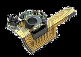
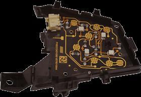
3 Thales products & mission profiles Main product characteristics Low volume (10-10k pcs/year) N 1 worldwide Heterogeneous Complex Dense boards Advanced technology as key differentiator Payloads for telecom satellites N 2 worldwide Air Traffic Management Sonars Security for interbank transactions Reparability Reliability Rail signalling systems In-flight entertainment and connectivity Military tactical radiocommunications Long mission profile Harsh environment N 3 worldwide Constraints Commercial avionics Civil satellites Military surface radars Dependency of civil market: dual technologies Need to launch manufacturing spread over long period Management of obsolescence Sourcing (PCB, EMS ): New technologies, specific processes & Export control 3

![Delta T [ C] Mechanical Shock and High Vibration Level Repair Needs Typical Volume per Product Batch Harsh](/docs-images/78/77887369/images/4-2.jpg "thermo-mechanical environment Harsh mechanical environment Mechanical shocks & vibrations Constraints far from")
 Military Avionics (a / b / c) 10 0.")
 Yes Yes 50 Telecom 7 to 20 0.01% -40 85 35 Yes Automotive under Hood 5 0.")
 20 (+40;+60;+80) Yes (rework) 3 1000 Yes No 100 000 Yes No 100 000 Computers 5 0.")
4 Thales products & mission profiles Reliability in harsh environment & long mission profiles Up to 35 years operation Use Category Typical years of Service Accepted Cumulated Failure within Lifetime Tmin [ C] Tmax [ C] Delta T [ C] Mechanical Shock and High Vibration Level Repair Needs Typical Volume per Product Batch Harsh thermo-mechanical environment Harsh mechanical environment Mechanical shocks & vibrations Constraints far from consumer electronic Space (leo / geo) 5 to % / 100 Yes Yes (rework) Military Avionics (a / b / c) % / 60 / 80 Yes Yes 10 Commercial Avionics % Yes Yes 200 Military Ground & Ship % (+60) Yes Yes 50 Telecom 7 to % Yes Automotive under Hood 5 0.1% Industrial & Automotive Passenger Compartment % (+100;+140) 20 (+40;+60;+80) Yes (rework) Yes No Yes No Computers 5 0.1% No No Consumer 1 to 3 1.0% No No Classification based on IPC-SM-785 High-Reliability Requirements Harsh Thermomechanical Environment Harsh Mechanical Environment Repairability Low Volume 4


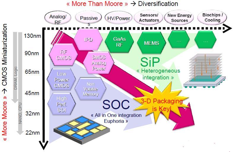


5 Packaging trend driven by Mobility / IoT Heterogeneity & density Sense, interact, power : complex heterogeneous integration PACKAGE key to adapt Compute & storage: complex design Agressive dimension reduction 5


6 SiP modules: key for complex/dense electronics SiP modules : paramount solution to make testability easier & improve yield Advantages Significantly increased board density Heterogeneous functionalities in a package Improved technical performances Reduced mother board complexity Re-usable module & reduction of development time Nb of Pts Aera mm² Nb of Pts/ dm² Top board With SIP Bottom board With SIP Shielded zone Constraints NRE in low volume Thermal management Complex supply chain management Obsolescence management Multi-sourcing Total density Total density with SIP Pts /dm² Pts/dm² SIP increase the total density by ~3 6


 Line/space (PCB) 1")
7 PCB and assembly trend PCB design trends driven by IC carrier PCB has to accommodate the latest packaging trends Finer pitch, increased I/O count: BGA, QFN, WLP packages, SiP modules Increased density by embedding components into PCB or Si carriers Increased challenge for solder mask years delay 7 10 Flip-chip pitch Package pitch Line/space (IC carrier) Line/space (PCB) HARTING TRW


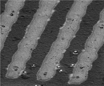

8 Conductor deposition on polymer Different processes like Molded Interconnect Devices Address the coupling electrical/mechanical Mature with one layer CITEC HARTING TRW Aerosol jet printing Fine line (typically 100µm) Multilayer under development Ink jet printing (2D) OPTOMEC Fine line (typically 100µm) Line definition function of drop size & surface energy OPTOMEC OPTOMEC NY Industries NY Industries 8
9 Supply & value chain evolutions Added value in packaging development Strong competition between IC foundries & PCB makers Heterogeneous integration at board level Increase the complexity of supply chain Wafer (FE) Packaging (BE) Electronic board Wafer level packages 3D modules, SiP Embedded passives & dies Fine pitch, heterogeneous, PoP, SiP + test Added value increase Procurement critical Foundry OSAT Back end PCB maker EMS OEM 9 Coupling must strongly increase Complex supply chain


10 Example of PCB embedding: complex supply chain Chip / wafer post-process required for PCB embedding RDL to adapt the die pitch to the PCB scale Wafer thinning Embedded resistor Cu plating: Pad finish must be copper Thermal management can require 2 Cu faces metallization Si dies procurement hard point for low volume Embedded active die Foundry OSAT PCB maker EMS OEM Ceramic chip 10 One board inside an equipment / system Active chip capacitor


11 3D IC packaging supply chain 11 Fast evolution in service offered, from SME to large providers Partner selection must fit with roadmap


 Reballing")
 Technology watch Early assessment (Eolane) Deployment of SnPb+ backward")
12 Focus on examples: PCBA technology / Lead-Free assembly 12 Lead-free assembly July 2006 entry into force of EU directive Long transition period 2002 Reballing & backward solution LF not yet used in harsh environments & for long mission profiles Backward SAC low Ag Interposer 2008 CATS project ( French MOD) Backward (mechanical stresses) PCB material LF compatible 2007 Cu dissolution 2006 Backward solders (low voids) Reballing 2005 Backward (Celestica corporate) Qualification fluxes, solder (pastes, wires) Technology watch Early assessment (Eolane) Deployment of SnPb+ backward process

13 Focus on examples: PCB technology / HDI boards with µvias HDI boards Development of test vehicles Incremental learning DfM & DfR establishment Collaboration with industrial & academic partner 13 Long development time for high-end applications Stacked µvias used in Thales products Only few & independent variables can be addressed at a time
14 Technology/process introduction into new products Reliability risk management is crucial before releasing a technology / process Strong coupling with partners Process maturity required before reliability assessment Dedicated toolbox & methodologies to evaluate technologies & processes 14


15 Tool box for advanced technologies / processes evaluation Supplier roadmaps Thales needs Test Methodologies Environmental Tests Failure Analysis Failure Analysis Test Vehicles Product Representative Test Vehicles Test definition Post Assembly Analysis Highly Accelerated Tests Failure Mode Analysis Return of Experience Comparison Failure Mechanisms Accelerated Test Conditions Mission Profile Definition Acceleration Factor Continuous Monitoring Specific Failure Criteria Statistical Analysis Finite Element Analysis Material Characterization Experimental Results Correlation 1 0,10 1,00 10,00 15


16 Establishment of DfM & DfR rules DfM & DfR rules establishment is performed through DoE Simulation is a very useful tool for To understand failure mechanism in complement to experimental DoE results To vary key parameters in a shorter time with a calibrated simulation model To substitute by sensitivity analysis an unknown physical parameter value 0.8mm pitch BGA100 overlapping embedded dies 16
17 Conclusions Packaging is a key differentiator for high density electronics & high reliability to: New generation of SIP are extremely complex Take the benefit of the huge evolution of the Si and III-V Mix technologies (MEMS, sensors, digital, analog, power ) Couple electronics & mechanics Manage the reliability risk including thermal management in harsh environment SIP / module using heterogeneous Technologies/Processes become mandatory Therefore: The supply chain is extremely complex Management of Heterogeneous bricks linked with different MRL In low volume, bare dies is a blocking point regarding procurement & Known Good Die For High end electronics Considering the fast evolution of T/P driven by mass product There is a strong need to develop T/P based on roadmap & in a frame of a network In partnership with labs, institutes, spin off, SME 17
18 Thank you
System in Package: Identified Technology Needs from the 2004 inemi Roadmap
 System in Package: Identified Technology Needs from the 2004 inemi Roadmap James Mark Bird Amkor Technology Inc System in package (SiP) technology has grown significantly in the past several years. It
Close supply chain collaboration enables easy implementation of chip embedded power SiP
 Close supply chain collaboration enables easy implementation of chip embedded power SiP Gerald Weidinger, R&D Project Leader, AT&S AT & S Austria Technologie & Systemtechnik Aktiengesellschaft Fabriksgasse13
Challenges and Solutions for Cost Effective Next Generation Advanced Packaging. H.P. Wirtz, Ph.D. MiNaPAD Conference, Grenoble April 2012
 Challenges and Solutions for Cost Effective Next Generation Advanced Packaging H.P. Wirtz, Ph.D. MiNaPAD Conference, Grenoble April 2012 Outline Next Generation Package Requirements ewlb (Fan-Out Wafer
Simulation of Embedded Components in PCB Environment and Verification of Board Reliability
 Simulation of Embedded Components in PCB Environment and Verification of Board Reliability J. Stahr, M. Morianz AT&S Leoben, Austria M. Brizoux, A. Grivon, W. Maia Thales Global Services Meudon-la-Forêt,
3D Package Technologies Review with Gap Analysis for Mobile Application Requirements. Apr 22, 2014 STATS ChipPAC Japan
 3D Package Technologies Review with Gap Analysis for Mobile Application Requirements Apr 22, 2014 STATS ChipPAC Japan T.Nishio Contents Package trends and roadmap update Advanced technology update Fine
System-in-Package (SiP) on Wafer Level, Enabled by Fan-Out WLP (ewlb)
 on Wafer Level, Enabled by Fan-Out WLP (ewlb)") System-in-Package (SiP) on Wafer Level, Enabled by Fan-Out WLP (ewlb) Steffen Kröhnert, José Campos, Eoin O Toole NANIUM S.A., Vila do Conde, Portugal Outline Short Company Overview NANIUM Introduction
System-in-Package (SiP) on Wafer Level, Enabled by Fan-Out WLP (ewlb) Steffen Kröhnert, José Campos, Eoin O Toole NANIUM S.A., Vila do Conde, Portugal Outline Short Company Overview NANIUM Introduction
Challenges for Embedded Device Technologies for Package Level Integration
 Challenges for Embedded Device Technologies for Package Level Integration Kevin Cannon, Steve Riches Tribus-D Ltd Guangbin Dou, Andrew Holmes Imperial College London Embedded Die Technology IMAPS-UK/NMI
Embedding Passive and Active Components: PCB Design and Fabrication Process Variations
 Embedding Passive and Active Components: PCB Design and Fabrication Process Variations Vern Solberg Solberg Technical Consulting Saratoga, California USA Abstract Embedding components within the PC board
Automotive Electronic Material Challenges. Anitha Sinkfield, Delphi
 Automotive Electronic Material Challenges Anitha Sinkfield, Delphi Automotive Electronic Material Challenges Project Update About inemi Project Participants Problem Statement Project Details Summary and
Innovative Substrate Technologies in the Era of IoTs
 Innovative Substrate Technologies in the Era of IoTs Dyi- Chung Hu 胡迪群 September 4, 2015 Unimicron Contents Introduction Substrate Technology - Evolution Substrate Technology - Revolution Glass substrate
RF System in Packages using Integrated Passive Devices
 RF System in Packages using Integrated Passive Devices by Kai Liu, YongTaek Lee, HyunTai Kim, Gwang Kim, and Billy Ahn STATS ChipPAC 1711 W. Greentree Drive, Suite #117, Tempe, AZ 85284, USA Tel: 480-222-1722
Semiconductor IC Packaging Technology Challenges: The Next Five Years
 SPAY025 May 2006 White Paper Mario A. Bolanos, Director Semiconductor Group Packaging Technology Development, Texas Instruments In the era of communications and entertainment, growth of consumer electronics
Wire-Bond CABGA A New Near Die Size Packaging Innovation Yeonho Choi February 1, 2017
 Amkor Technology, Inc. White Paper Wire-Bond CABGA A New Near Die Size Packaging Innovation Yeonho Choi February 1, 2017 Abstract Expanding its ChipArray Ball Grid Array (CABGA) package form factor miniaturization
Silicon Interposers with Integrated Passive Devices: Ultra-Miniaturized Solution using 2.5D Packaging Platform
 Minapad 2014, May 21 22th, Grenoble; France Silicon Interposers with Integrated Passive Devices: Ultra-Miniaturized Solution using 2.5D Packaging Platform Stéphane Bellenger, Laëtitia Omnès, Jean-René
Cost effective 300mm Large Scale ewlb (embedded Wafer Level BGA) Technology
 Technology") Cost effective 300mm Large Scale ewlb (embedded Wafer Level BGA) Technology by Meenakshi Prashant, Seung Wook Yoon, Yaojian LIN and Pandi C. Marimuthu STATS ChipPAC Ltd. 5 Yishun Street 23, Singapore 768442
Cost effective 300mm Large Scale ewlb (embedded Wafer Level BGA) Technology by Meenakshi Prashant, Seung Wook Yoon, Yaojian LIN and Pandi C. Marimuthu STATS ChipPAC Ltd. 5 Yishun Street 23, Singapore 768442
Chips Face-up Panelization Approach For Fan-out Packaging
 Chips Face-up Panelization Approach For Fan-out Packaging Oct. 15, 2015 B. Rogers, D. Sanchez, C. Bishop, C. Sandstrom, C. Scanlan, TOlson T. REV A Background on FOWLP Fan-Out Wafer Level Packaging o Chips
Pb-free Challenges for High Complexity Products. inemi Jan 16 th 2008
 Pb-free Challenges for High Complexity Products inemi Jan 16 th 2008 All Rights Reserved Alcatel-Lucent 2007 Agenda RoHS 101 Typical complex of telecom products (different from consumable) Pb-free Concerns
Modelling Embedded Die Systems
 Modelling Embedded Die Systems Stoyan Stoyanov and Chris Bailey Computational Mechanics and Reliability Group (CMRG) University of Greenwich, London, UK 22 September 2016 IMAPS/NMI Conference on EDT Content
Novel Materials and Activities for Next Generation Package. Hitachi Chemical., Co.Ltd. Packaging Solution Center Hiroaki Miyajima
 Novel Materials and Activities for Next Generation Package Hitachi Chemical., Co.Ltd. Packaging Solution Center Hiroaki Miyajima 1. Activities of Packaging Solution Center 2. Novel Materials for Next Gen.
Chip Packaging for Wearables Choosing the Lowest Cost Package
 Chip Packaging for Wearables Choosing the Lowest Cost Package Alan Palesko alanp@savansys.com (512) 402-9943 www.savansys.com Slide - 1 Agenda Introduction Wearable Requirements Packaging Technologies
YOUR Strategic TESTING ENGINEERING CONCEPT SMT FLIP CHIP PRODUCTION OPTO PACKAGING PROCESS DEVELOPMENT CHIP ON BOARD SUPPLY CHAIN MANAGEMENT
 YOUR Strategic TECHNOLOGY PARTNER Wafer Back-End OPTO PACKAGING PROCESS DEVELOPMENT CONCEPT FLIP CHIP PROTOTYping ENGINEERING TESTING SMT PRODUCTION CHIP ON BOARD SUPPLY CHAIN MANAGEMENT Next Level 0f
Open-Sourcing the Model-Based Systems Engineering Solution Capella
 Open-Sourcing the Model-Based Systems Engineering Solution Capella C. Boudjennah 1, B. Combemale 2, D. Exertier 3, Matthieu Helleboid 3, S. Lacrampe 1, M.A Peraldi-Frati 4 1 Obeo 2 University of Rennes
Panel Discussion: Advanced Packaging
 Dr. Steve Bezuk Senior Director IC Packaging Engineering Qualcomm Technologies, Inc. Panel Discussion: Advanced Packaging PAGE 1 Technical Challenges of Packaging (Mobile Focus) Materials Die materials
Basic PCB Level Assembly Process Methodology for 3D Package-on-Package
 Basic PCB Level Assembly Process Methodology for 3D Package-on-Package Vern Solberg STC-Madison Madison, Wisconsin USA Abstract The motivation for developing higher density IC packaging continues to be
Roundtable 3DIC & TSV: Ready for HVM? European 3D TSV Summit
 Roundtable 3DIC & TSV: Ready for HVM? European 3D TSV Summit Infineon VTI Xilinx Synopsys Micron CEA LETI 2013 Yann Guillou Business Development Manager Lionel Cadix Market & Technology Analyst, Advanced
Graser User Conference Only
 2.5D/3D Design Solution Eric Chen & Scott Liu 31/Oct/2014 Roadmap data is provided for informational purposes only and does not represent a commitment to deliver any of the features or functionality discussed
Board Level Reliability Improvement in ewlb (Embedded Wafer Level BGA) Packages
 Packages") Board Level Reliability Improvement in ewlb (Embedded Wafer Level BGA) Packages by Seng Guan Chow, Yaojian Lin, Bernard Adams * and Seung Wook Yoon** STATS ChipPAC Ltd. 5 Yishun Street 23, Singapore 768442
Board Level Reliability Improvement in ewlb (Embedded Wafer Level BGA) Packages by Seng Guan Chow, Yaojian Lin, Bernard Adams * and Seung Wook Yoon** STATS ChipPAC Ltd. 5 Yishun Street 23, Singapore 768442
"ewlb Technology: Advanced Semiconductor Packaging Solutions"
 "ewlb Technology: Advanced Semiconductor Packaging Solutions" by Sharma Gaurav@, S.W. Yoon, Yap Yok Mian, Shanmugam Karthik, Yaojian Lin, Pandi C. Marimuthu and Yeong J. Lee* STATS ChipPAC Ltd. 5 Yishun
SEMI MEMS Tech Seminar (Sept 26, Cornaredo, Italy)
") SEMI MEMS Tech Seminar (Sept 26, 2013 - Cornaredo, Italy) Opportunities of Wafer Level Embedded Technologies for MEMS Devices T. Braun ( 1 ), K.-F. Becker ( 1 ), R. Kahle ( 2 ), V. Bader ( 1 ), S. Voges
SEMI MEMS Tech Seminar (Sept 26, 2013 - Cornaredo, Italy) Opportunities of Wafer Level Embedded Technologies for MEMS Devices T. Braun ( 1 ), K.-F. Becker ( 1 ), R. Kahle ( 2 ), V. Bader ( 1 ), S. Voges
Capella on the field: Model-based system engineering use cases
 www.thalesgroup.com Capella on the field: Model-based system engineering use cases EclipseCon Europe 2014 Ludwigsburg, October 29 th, 2014 Christophe Gatti (Thales Corporate Engineering) Matthieu Helleboid
Design for Flip-Chip and Chip-Size Package Technology
 Design for Flip-Chip and Chip-Size Package Technology Vern Solberg Solberg Technology Consulting Madison, Wisconsin Abstract As new generations of electronic products emerge they often surpass the capability
Development of System in Package
 Development of System in Package In recent years, there has been a demand to offer increasingly enhanced performance for a SiP that implements downsized and lower-profile chips at lower cost. This article
System Level Effects on Solder Joint Reliability
 System Level Effects on Solder Joint Reliability Maxim Serebreni 2004 2010 Outline Thermo-mechanical Fatigue of solder interconnects Shear and tensile effects on Solder Fatigue Effect of Glass Style on
The 3D Silicon Leader
 The 3D Silicon Leader TSV technology embedding high density capacitors for advanced 3D packaging solutions IMAPS Device Packaging Conference 2014 Catherine Bunel 2014.03.12 Outline Introduction IPDiA s
IMPACT OF LEAD-FREE COMPONENTS AND TECHNOLOGY SCALING FOR HIGH RELIABILITY APPLICATIONS
 IMPACT OF LEAD-FREE COMPONENTS AND TECHNOLOGY SCALING FOR HIGH RELIABILITY APPLICATIONS Chris Bailey, Ph.D. University of Greenwich London, United Kingdom c.bailey@gre.ac.uk ABSTRACT Semiconductor technology
9 rue Alfred Kastler - BP Nantes Cedex 3 - France Phone : +33 (0) website :
 website :") 9 rue Alfred Kastler - BP 10748-44307 Nantes Cedex 3 - France Phone : +33 (0) 240 180 916 - email : info@systemplus.fr - website : www.systemplus.fr February 2012 - Version 1 Written by: Romain FRAUX DISCLAIMER
9 rue Alfred Kastler - BP 10748-44307 Nantes Cedex 3 - France Phone : +33 (0) 240 180 916 - email : info@systemplus.fr - website : www.systemplus.fr February 2012 - Version 1 Written by: Romain FRAUX DISCLAIMER
IMPLEMENTATION OF A FULLY MOLDED FAN-OUT PACKAGING TECHNOLOGY
 IMPLEMENTATION OF A FULLY MOLDED FAN-OUT PACKAGING TECHNOLOGY B. Rogers, C. Scanlan, and T. Olson Deca Technologies, Inc. Tempe, AZ USA boyd.rogers@decatechnologies.com ABSTRACT Fan-Out Wafer-Level Packaging
Ultralow Residue Semiconductor Grade Fluxes for Copper Pillar Flip-Chip
 Ultralow Residue Semiconductor Grade Fluxes for Copper Pillar Flip-Chip SzePei Lim (Presenter), Jason Chou, Maria Durham, and Dr. Andy Mackie Indium Corporation 1 Outline of Presentation Roadmaps and challenges
EPOXY FLUX MATERIAL AND PROCESS FOR ENHANCING ELECTRICAL INTERCONNECTIONS
 As originally published in the SMTA Proceedings. EPOXY FLUX MATERIAL AND PROCESS FOR ENHANCING ELECTRICAL INTERCONNECTIONS Neil Poole, Ph.D., Elvira Vasquez, and Brian J. Toleno, Ph.D. Henkel Electronic
Advances in Printing nano Cu and Using Existing Cu Based Manufacturing Processes. Michael J. Carmody Chief Scientist, Intrinsiq Materials
 Advances in Printing nano Cu and Using Existing Cu Based Manufacturing Processes Michael J. Carmody Chief Scientist, Intrinsiq Materials Why Use Copper? Lower Cost than Silver. Print on Numerous Substrates.
Thermo-Mechanical FEM Analysis of Lead Free and Lead Containing Solder for Flip Chip Applications
 Thermo-Mechanical FEM Analysis of Lead Free and Lead Containing Solder for Flip Chip Applications M. Gonzalez 1, B. Vandevelde 1, Jan Vanfleteren 2 and D. Manessis 3 1 IMEC, Kapeldreef 75, 3001, Leuven,
3D-WLCSP Package Technology: Processing and Reliability Characterization
 3D-WLCSP Package Technology: Processing and Reliability Characterization, Paul N. Houston, Brian Lewis, Fei Xie, Ph.D., Zhaozhi Li, Ph.D.* ENGENT Inc. * Auburn University ENGENT, Inc. 2012 1 Outline Packaging
PCB/PCBA Material Characterization for Automotive Harsh Environments
 PCB/PCBA Material Characterization for Automotive Harsh Environments Project Chair: Steve Brown MacDermid Performance Solutions inemi Staff: Steve Payne Agenda Introduction of Project Chair and inemi Project
Nondestructive Internal Inspection. The World s Leading Acoustic Micro Imaging Lab
 Nondestructive Internal Inspection The World s Leading Acoustic Micro Imaging Lab Unmatched Capabilities and Extensive Expertise At Your Service SonoLab, a division of Sonoscan, is the world s largest
Power Electronics Packaging Revolution Module without bond wires, solder and thermal paste
 SEMIKRON Pty Ltd 8/8 Garden Rd Clayton Melbourne 3168 VIC Australia Power Electronics Packaging Revolution Module without bond wires, solder and thermal paste For some years now, the elimination of bond
Low Temperature Co-fired Ceramics (LTCC) Multi-layer Module Boards
 Multi-layer Module Boards") Low Temperature Co-fired Ceramics () Multi-layer Module Boards Example: Automotive Application Example: Communication Application Murata's Low Temperature Co-fired Ceramics offer highly integrated substrates
Low Temperature Co-fired Ceramics () Multi-layer Module Boards Example: Automotive Application Example: Communication Application Murata's Low Temperature Co-fired Ceramics offer highly integrated substrates
IMPACT OF MICROVIA-IN-PAD DESIGN ON VOID FORMATION
 IMPACT OF MICROVIA-IN-PAD DESIGN ON VOID FORMATION Frank Grano, Felix Bruno Huntsville, AL Dana Korf, Eamon O Keeffe San Jose, CA Cheryl Kelley Salem, NH Joint Paper by Sanmina-SCI Corporation EMS, GTS
AEC WORK SHOP SESSION KNOWN GOOD DIE / MULTI-CHIP MODULE. Daniel Vanderstraeten On Semiconductor
 AEC WORK SHOP SESSION KNOWN GOOD DIE / MULTI-CHIP MODULE Banjie Bautista - Integrated Silicon Solution Inc. Pamela Finer Pericom Semiconductor Tim Haifley Altera Tom Lawler Lattice Semiconductor Nick Lycoudes
Advancements In Packaging Technology Driven By Global Market Return. M. G. Todd
 Advancements In Packaging Technology Driven By Global Market Return M. G. Todd Electronic Materials, Henkel Corporation, Irvine, California 92618, USA Recently, the focus of attention in the IC packaging
White Paper Quality and Reliability Challenges for Package on Package. By Craig Hillman and Randy Kong
 White Paper Quality and Reliability Challenges for Package on Package By Craig Hillman and Randy Kong Background Semiconductor technology advances have been fulfilling Moore s law for many decades. However,
The Packaging and Reliability Qualification of MEMS Resonator Devices
 The Packaging and Reliability Qualification of MEMS Resonator Devices Pavan Gupta Vice President, Operations Yin-Chen Lu, Preston Galle Quartz and MEMS Oscillators source: www.ecliptek.com Quartz Oscillators:
Packaging Substrate Workshop Wrap Up. Bob Pfahl, inemi
 Packaging Substrate Workshop Wrap Up Bob Pfahl, inemi Warpage Facilitator: Jie Xue, Cisco Presenter: ML Loke, Intel Breakout Session (ends 10:30 am) Introduction & your expectation Issues & Root cause
Samsung 3D TSV Stacked DDR4 DRAM
 Samsung 3D TSV Stacked DDR4 DRAM The First Memory product with Via-Middle TSV! 3D TSV technology is expected to reach $4.8B in revenues by 2019, mainly driven by 3D stacked DRAM and followed by 3D Logic/Memory
3D Integrated ewlb /FO-WLP Technology for PoP & SiP
 3D Integrated ewlb /FO-WLP Technology for PoP & SiP by Yaojian Lin, Chen Kang, Linda Chua, Won Kyung Choi and *Seung Wook Yoon STATS ChipPAC Pte Ltd. 5 Yishun Street 23, Singapore 768442 *STATS ChipPAC
Copper Wire Packaging Reliability for Automotive and High Voltage
 Copper Wire Packaging Reliability for Automotive and High Voltage Tu Anh Tran AMPG Package Technology Manager Aug.11.2015 TM External Use Agenda New Automotive Environments Wire Bond Interconnect Selection
Semiconductor Packaging and Assembly 2002 Review and Outlook
 Gartner Dataquest Alert Semiconductor Packaging and Assembly 2002 Review and Outlook During 2002, the industry continued slow growth in unit volumes after bottoming out in September 2001. After a hearty
Three-Dimensional Molded Interconnect Devices (3D-MID)
") Jörg Frank Three-Dimensional Molded Interconnect Devices (3D-MID) Materials, Manufacturing, Assembly and Applica ons for Injec on Molded Circuit Carriers Sample Pages ISBN 978-1-56990-551-7 HANSER Hanser
Jörg Frank Three-Dimensional Molded Interconnect Devices (3D-MID) Materials, Manufacturing, Assembly and Applica ons for Injec on Molded Circuit Carriers Sample Pages ISBN 978-1-56990-551-7 HANSER Hanser
Non-Hermetic Packaging of RF Multi-Chip Modules
 Non-Hermetic Packaging of RF Multi-Chip Modules Matthew Gruber Lockheed Martin MST Moorestown, NJ 1 A Comment about this Presentation In accordance with ITAR restrictions, a few concessions had to be made
Advanced Analytical Techniques for Semiconductor Assembly Materials and Processes. Jason Chou and Sze Pei Lim Indium Corporation
 Advanced Analytical Techniques for Semiconductor Assembly Materials and Processes Jason Chou and Sze Pei Lim Indium Corporation Agenda Company introduction Semiconductor assembly roadmap challenges Fine
FLIP CHIP CHIP ON BOARD SMT ENGINEERING OPTO PACKAGING SUPPLY CHAIN MANAGEMENT TESTING YOUR INNOVATIVE TECHNOLOGY PARTNER PRODUCTION CONCEPT
 YOUR INNOVATIVE TECHNOLOGY PARTNER CHIP ON BOARD OPTO PACKAGING PROCESS DEVELOPMENT CONCEPT FLIP CHIP ENGINEERING TESTING PRODUCTION SMT SUPPLY CHAIN MANAGEMENT PROTOTYPES HIGH-PRECISION ASSEMBLY OF MICRO-
Silicon Wafer Processing PAKAGING AND TEST
 Silicon Wafer Processing PAKAGING AND TEST Parametrical test using test structures regularly distributed in the wafer Wafer die test marking defective dies dies separation die fixing (not marked as defective)
OHMEGA-PLY INTEGRAL PLANAR RESISTORS: THE LOWER COST ALTERNATIVE By Daniel Brandler Ohmega Technologies, Inc.
 OHMEGA-PLY INTEGRAL PLANAR RESISTORS: THE LOWER COST ALTERNATIVE By Daniel Brandler Ohmega Technologies, Inc. Printed circuit board designers are being forced to interconnect electronic devices of increasing
NXP SCM-i.MX6 Quad High Density Fan-Out Wafer-Level System-in-Package
 NXP SCM-i.MX6 Quad High Density Fan-Out Wafer-Level System-in-Package The first ultra-small multi-die low power module with boot memory and power management integrated in a package-on-package compatible
FRAUNHOFER INSTITUTE FOR RELIABILITY AND MICROINTEGRATION IZM DEPARTMENT WAFER LEVEL SYSTEM INTEGRATION BERLIN
 FRAUNHOFER INSTITUTE FOR RELIABILITY AND MICROINTEGRATION IZM DEPARTMENT WAFER LEVEL SYSTEM INTEGRATION BERLIN WAFER LEVEL SYSTEM INTEGRATION ELECTRONIC PACKAGING AT FRAUNHOFER IZM The Fraunhofer Institute
IPC-AJ-820A Assembly and Joining Handbook. The How and Why of All Things PCB & PCA
 IPC-AJ-820A Assembly and Joining Handbook The How and Why of All Things PCB & PCA 1 Scope To provide guidelines and supporting info for the mfg of electronic equipment To explain the HOW TO and WHY Discussions
WF6317. A superactive low-volatile/high heat-resistant water-soluble flux for ball soldering
 WF637 A superactive low-volatile/high heat-resistant water-soluble flux for ball soldering Low viscosity and high tacking power stabilize ball holding force and ensures excellent solder wettability Easy
Evaluation of Cu Pillar Chemistries
 Presented at 2016 IMAPS Device Packaging Evaluation of Cu Pillar Chemistries imaps Device Packaging Conference Spring 2016 Matthew Thorseth, Mark Scalisi, Inho Lee, Sang-Min Park, Yil-Hak Lee, Jonathan
Electronic Costing & Technology Experts
 Electronic Costing & Technology Experts 21 rue la Nouë Bras de Fer 44200 Nantes France Phone : +33 (0) 240 180 916 email : info@systemplus.fr www.systemplus.fr May 2013 Version 1 Written by Romain Fraux
TSV CHIP STACKING MEETS PRODUCTIVITY
 TSV CHIP STACKING MEETS PRODUCTIVITY EUROPEAN 3D TSV SUMMIT 22-23.1.2013 GRENOBLE HANNES KOSTNER DIRECTOR R&D BESI AUSTRIA OVERVIEW Flip Chip Packaging Evolution The Simple World of C4 New Flip Chip Demands
Highly Accelerated Thermal Shock Reliability Testing
 Highly Accelerated Thermal Shock Reliability Testing by Bob E. Neves Microtek Laboratories, Inc. Anaheim CA and Rick B. Snyder Delphi Delco Electronics Systems, Inc. Kokomo IN and Timothy A. Estes Conductor
Coil on Module. Packaging innovation for egov documents.
 Coil on Module Packaging innovation for egov documents www.infineon.com/com Abstract Modern ID cards are required to stand up to many types of stress, ranging from attempts at physical alteration, to wear
Development of Exposed Die Large Body to Die Size Ratio Wafer Level Package Technology
 Development of Exposed Die Large Body to Die Size Ratio Wafer Level Package Technology by J. Osenbach 1, S. Emerich1, L. Golick1, S. Cate 2, M. Chan3, S.W. Yoon 3, Y.J. Lin 4 & K. Wong 5, 1LSI Corporation
Board Assembly MANUFACTURING TECHNOLOGIES. Wave and Selective Soldering... 48
 Board Assembly Dr. Dongkai Shangguan, Flextronics, Chair Dr. Ravi Bhatkal, Cookson Electronics, Co-Chair David Geiger, Flextronics, Co-Chair CONTENTS: Board Assembly... 1 Executive Summary... 1 Introduction...
ALTERNATIVES TO SOLDER IN INTERCONNECT, PACKAGING, AND ASSEMBLY
 ALTERNATIVES TO SOLDER IN INTERCONNECT, PACKAGING, AND ASSEMBLY Herbert J. Neuhaus, Ph.D., and Charles E. Bauer, Ph.D. TechLead Corporation Portland, OR, USA herb.neuhaus@techleadcorp.com ABSTRACT Solder
TSV Interposer Process Flow with IME 300mm Facilities
 TSV Interposer Process Flow with IME 300mm Facilities Property of Institute of Microelectronics (IME)-Singapore August 17, 2012 Outline 1. TSV interposer (TSI) cross sectional schematic TSI with BEOL,
Alternative Approaches to 3-Dimensional Packaging and Interconnection
 Alternative Approaches to 3-Dimensional Packaging and Interconnection Joseph Fjelstad SiliconPipe, Inc. www.sipipe.com IC Packaging a Technology in Transition In the past, IC packaging has been considered
Prime Technology Inc.(PTI), Engineering Capability
, Engineering Capability") Technology, Knowhow, Services & Market Segments With large-scale resources and the broadest capital in the Electronics Manufacturing Services (EMS) industry, Prime Technology (PTI) provides services from
Technology, Knowhow, Services & Market Segments With large-scale resources and the broadest capital in the Electronics Manufacturing Services (EMS) industry, Prime Technology (PTI) provides services from
Thermo-Mechanical Reliability Assessment of TSV Die Stacks by Finite Element Analysis
 Thermo-Mechanical Reliability Assessment of TSV Die Stacks by Finite Element Analysis Dr. Roland Irsigler, emens AG Corporate Technology, CT T P HTC Outline TSV SOLID µbump Stacking TSV application FEA
Statement of Work (SOW) inemi Board Assembly TIG BiSn-Based Low-Temperature Soldering Process and Reliability Project
 inemi Board Assembly TIG BiSn-Based Low-Temperature Soldering Process and Reliability Project") Statement of Work (SOW) inemi Board Assembly TIG BiSn-Based Low-Temperature Soldering Process and Reliability Project Version 1.4 Date: December 1, 2015 Project Leader: Raiyo Aspandiar, Intel Corporation
Statement of Work (SOW) inemi Board Assembly TIG BiSn-Based Low-Temperature Soldering Process and Reliability Project Version 1.4 Date: December 1, 2015 Project Leader: Raiyo Aspandiar, Intel Corporation
Test Flow for Advanced Packages (2.5D/SLIM/3D)
") 1 Test Flow for Advanced Packages (2.5D/SLIM/3D) Gerard John Amkor Technology Inc. Gerard.John@amkor.com 2045 East Innovation Circle, Tempe, AZ 85284, USA Phone: (480) 821-5000 ADVANCED PACKAGE TEST FLOW
1 Test Flow for Advanced Packages (2.5D/SLIM/3D) Gerard John Amkor Technology Inc. Gerard.John@amkor.com 2045 East Innovation Circle, Tempe, AZ 85284, USA Phone: (480) 821-5000 ADVANCED PACKAGE TEST FLOW
Packaging Commercial CMOS Chips for Lab on a Chip Integration
 Supporting Information for Packaging Commercial CMOS Chips for Lab on a Chip Integration by Timir Datta-Chaudhuri, Pamela Abshire, and Elisabeth Smela Biocompatibility Although the supplier s instructions
Package Solutions and Innovations
 Package Solutions and Innovations with Compression Molding IEEE SVC CPMT Aug 2015 Presented by C.H. Ang Towa USA Company Profile www.cpmt.org/scv 1 Corporate Overview Company: Towa Corp., Kyoto Japan Established:
Qualification and Performance Specification for Flexible Printed Boards
 Qualification and Performance Specification for Flexible Printed Boards Developed by the Flexible Circuits Performance Specifications Subcommittee (D-12) of the Flexible Circuits Committee (D-10) of IPC
3D technologies for integration of MEMS
 3D technologies for integration of MEMS, Fraunhofer Institute for Electronic Nano Systems Folie 1 Outlook Introduction 3D Processes Process integration Characterization Sample Applications Conclusion Folie
2.5D and 3D Semiconductor Package Technology: Evolution and Innovation
 2.5D and 3D Semiconductor Package Technology: Evolution and Innovation Vern Solberg Solberg Technical Consulting Saratoga, California USA Abstract The electronics industry is experiencing a renaissance
Silicon Interposer with Embedded Microfluidic Cooling for High-Performance Computing Systems
 Silicon Interposer with Embedded Microfluidic Cooling for High-Performance Computing Systems Li Zheng 1, Yang Zhang, Xuchen Zhang and Muhannad S. Bakir 2 School of Electrical and Computer Engineering Georgia
Thin Wafers Bonding & Processing
 Thin Wafers Bonding & Processing A market perspective 2012 Why New Handling Technologies Consumer electronics is today a big driver for smaller, higher performing & lower cost device configurations. These
Power Electronics Packaging Solutions for Device Junction Temperature over 220 o C
 EPRC 12 Project Proposal Power Electronics Packaging Solutions for Device Junction Temperature over 220 o C 15 th August 2012 Page 1 Motivation Increased requirements of high power semiconductor device
FABRICATION AND RELIABILITY OF ULTRA-FINE RDL STRUCTURES IN ADVANCED PACKAGING BY EXCIMER LASER ABLATION
 FABRICATION AND RELIABILITY OF ULTRA-FINE RDL STRUCTURES IN ADVANCED PACKAGING BY EXCIMER LASER ABLATION NCCAVS Joint Users Group Technical Symposium San Jose, June 7 th, 2017 Markus Arendt, SÜSS MicroTec
Thales further strengthens its digital leadership thanks to the acquisition of Guavus 28 April 2017
 Thales further strengthens its digital leadership thanks to the acquisition of Guavus 28 April 2017 www.thalesgroup.com Digital transformation: a key growth opportunity for Thales Building a growing, more
TSV Processing and Wafer Stacking. Kathy Cook and Maggie Zoberbier, 3D Business Development
 TSV Processing and Wafer Stacking Kathy Cook and Maggie Zoberbier, 3D Business Development Outline Why 3D Integration? TSV Process Variations Lithography Process Results Stacking Technology Wafer Bonding
Copyright 2009 Year IEEE. Reprinted from 2009 Electronic Components and Technology Conference. Such permission of the IEEE does not in any way imply
 Copyright 2009 Year IEEE. Reprinted from 2009 Electronic Components and Technology Conference. Such permission of the IEEE does not in any way imply IEEE endorsement of any of Institute of Microelectronics
MATERIALS. September Construction Profiles and Material Decomposition p.18. Improved Thin-Film Resistor Material p.24
 September 2013 Construction Profiles and Material Decomposition p.18 MATERIALS Improved Thin-Film Resistor Material p.24 High-Frequency Laminates for Hybrid Multilayer PCBs p.30 Material Selection for
Material Selection and Parameter Optimization for Reliable TMV Pop Assembly
 Selection and Parameter Optimization for Reliable TMV Pop Assembly Brian Roggeman, David Vicari Universal Instruments Corp. Binghamton, NY, USA Roggeman@uic.com Martin Anselm, Ph.D. - S09_02.doc Lee Smith,
Manufacturing and Reliability Modelling
 Manufacturing and Reliability Modelling Silicon Chip C Bailey University of Greenwich London, England Printed Circuit Board Airflow Temperature Stress at end of Reflow Stress Product Performance in-service
Fanout Flipchip ewlb (embedded Wafer Level Ball Grid Array) Technology as 2.5D Packaging Solution
 Technology as 2.5D Packaging Solution") Fanout Flipchip ewlb (embedded Wafer Level Ball Grid Array) Technology as 2.5D Packaging Solution by Seung Wook Yoon,*Patrick Tang, **Roger Emigh, Yaojian Lin, Pandi C. Marimuthu, and *Raj Pendse STATS
Fanout Flipchip ewlb (embedded Wafer Level Ball Grid Array) Technology as 2.5D Packaging Solution by Seung Wook Yoon,*Patrick Tang, **Roger Emigh, Yaojian Lin, Pandi C. Marimuthu, and *Raj Pendse STATS
3D Packaging- Synthetic Quartz Substrate and Interposers for High Frequency Applications. Vern Stygar #1, Tim Mobley* 2 # Asahi Glass Corporation
 3D Packaging- Synthetic Quartz Substrate and Interposers for High Frequency Applications Vern Stygar #1, Tim Mobley* 2 # Asahi Glass Corporation 4375 Northwest 235 th Avenue, Hillsboro OR USA 97124 1 vstygar@agem.com