Development of Conductive Polymer Film and R2R Coating Process
|
|
|
- Laurence Chandler
- 5 years ago
- Views:
Transcription
1 Development of Conductive Polymer Film and R2R Coating Process Nizamidin Jappar; Ph.D. General Manager of R&D Kimoto Tech Inc. AIMCAL Web Coating & Handling Conference

2 Outline 1 Background Develop a conductive polymer film Scratch resistance film Future plan
3 1 Background


4 Multiple High Growth Markets Opportunity for conductive Film

5 Market and Manufacturing Directions Thinner, Lighter. Large display area. Flexible, Rugged. Touch interface. Lower cost.
6 Why R2R Manufacturing? Flexible Formable Weight Ruggedness High cost Low Cost Roll-to-Roll Production? Because it may be essential to enable the high volume applications of flexible displays!
7 Key Issues: ITO film 1. Brittle Limited Compatibility with Flexible Devices bending results in increased sheet resistance 2. Requires expensive vacuum based deposition process Increases MFG Complexity / Cost 3. Inorganic material: Indium is a rare metal Significant Price Fluctuations ($250 to $1000 per kg)

 Carbon")
8 Opportunity for ITO Alternative Conductive Polymer (CP) Silver Nanowires (SNW) Carbon Nanotube (CNT)
9 Characteristics Material Mfg. method Cost Resistivity Ω/sq Transparent Flexibility ITO Dry X X CNT Wet SNW Wet CP Wet


10 Flexible Electrodes Enhances New Applications Extraordinary Readability All lighting conditions Any illumination angle Ultra-Low Power Zero-Power Image Stability Exceptional Portability Thin, Light & Rugged Touch panel (sensor) Low-Risk Manufacturing Uses existing display infrastructure -materials, components & processes Simple assembly Fast-to-Market with minimal capital
11 2 Develop a conductive polymer film
12 Chemical structure of PEDOT/PSS O S O + SO 3 H y Na 2 S 2 O 8 (Fe 2 (SO 4 ) 3 ) H 2 O H O S O O O O O O O O O + + S S S H S SO 3 H SO 3 - SO 3 H SO 3 - SO 3 H "EDOT" Poly(3,4-ethylene dioxylene thiophene) "PEDOT/PSSA" Poly(4-styrene sulfonic acid) Orgacon is the trade name for Agfa Materials conductive polymer product line. The active component in Orgacon products is the water based electronic conductive polymer dispersion PEDOT/PSS (polyethylene dioxythiophene).
13 Conductive Polymer Coating Process 1. Formulation: Additive 2. Primer coating 3. Corona treatment
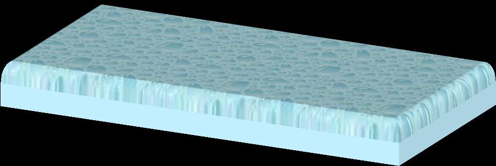
14 Factors for Water Resistance Additive Thick ness Temp. Drying Time Water Resistance What is Main Factor? Quantitative Evaluation
15 Main Factor for Water Resistance W = x A 1.0 x H -1.5 x T 2.0 x θ 1.2 A : Amount of Additive H : Thickness T : Temperature θ : Time Drying Condition is the most important factor
16 Calc. Resistivity Calc. Resistivity Main Factor for Resistivity Calc. Calculation 0% 10% 0 % +10 % - 10 % -10% Exp. Resistivity Exp. Resistivity

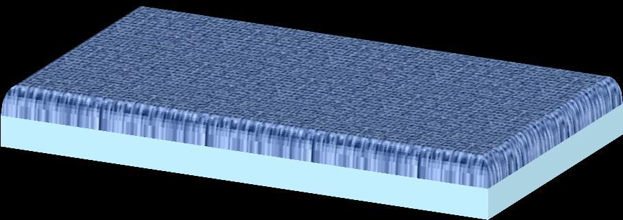
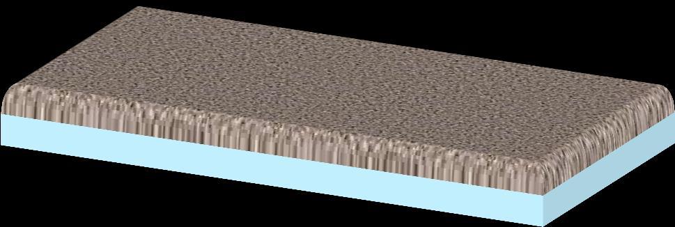
17 Cross-web Surface Resistivity Uniformity Conductive film
 300-500 450 450 VLT (%) on 188µm PET > 86-90% 91,4% 90% Stability (ratio R/R0) 240hr@60 C/90%RH <1,1 1,3 0,9 240hr@80 C <1,1 1,4 0,8 Temperature &")
18 Key property : low surface resistance high VLT Different formulation types Coating formulations & coated film Property ITO Orgacon S305 Orgacon S305plus SER (Ohm/sq) VLT (%) on 188µm PET > 86-90% 91,4% 90% Stability (ratio R/R0) 240hr@60 C/90%RH <1,1 1,3 0,9 240hr@80 C <1,1 1,4 0,8 Temperature & UVstabilized
19 SELECTION of Support PET SER Ohm/s q VLT% (hazeguar d) a* b* Haze % Optical grade PET Ref S305plus

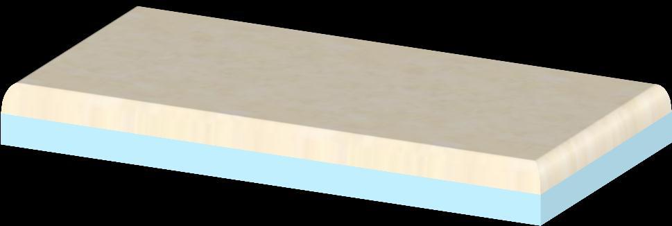
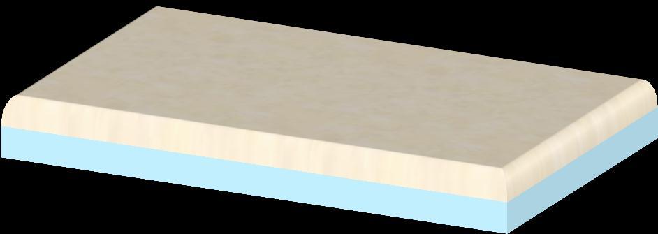
20 Ohmlex Film Conductive Polymer Coated Film
21 3 Scratch resistance film
22 Protective Film Applications A scratch resistance surface on appliances that must be resistant to chemical household cleaning Protective film used for touch screen, membrane switch and electronic display surface protection An abrasion resistant over laminate for signage and display applications Protective film for LCD, plasma and other flat screen displays UV protective film for solar and photovoltaic uses Adhesive protective film Scratch-resistant over laminates for printed labels


23 Development Concept of KTI UV Hard Coat Film Both side Coating Anti-finger Print ADDITIONAL One side Coating Structure Hardness/ Flexibility Properties Conductive /UVHC UV absorb Oligomer Monomers Clear Hard Coating Formulation Additives Surface Matte Solvents Texture Base Technology Surface Technology
24 KTI UV Hard Coated Film Properties Haze Optical Gloss Adhesion Chemical Surface E Transmittance Hardness Physical Flexibility
25 Anti-Fingerprint UV Hard Coated Film Formulation : Acrylic polymer 30 % Pigment A : 1~ 15 µm, 1 ~ 3 % Pigment A : 5~ 50 nm, 1 ~ 3 % Photo initiators: 1 ~ 2 % Properties : Surface tension 25 mn/m ~ Ra 0.05 µm ~ Rz 0.2 ~ 2.0 µm Haze: 1.5 % ~ Hardness: 2H Finger print: less visible & easy wipe out
26 Urea Lactic acid Sodium pyrophosphate Sodium chloride Ethanol Water Formulation of Artificial Fingerprint Solution

27 KTI Anti-sparkle Hard Coated Film KTI utilises an Anti Glare coating on the PET; which is exactly the same as an Anti Reflective coating, designed to eliminate reflection and subsequent interference with the image presented to the user. 01 AFP side is for surface of case, and it has a property of easy to wipe our the finger Surface print. Glass


28 Adjust each layers reflective index Eliminates reflected light and maximizes transmitted light in an optical system. Ƞ air < ƞ 01AFP < ƞ 02A < ƞ glass


29 Kimoto Tech UV Hard Coated PET

30 Kimoto Tech UV Stabilized, UV Hard Coated PET


31 Kimoto Tech UV Hard Coated PC

32 KTI Product Offering For Touch Applications Ohmlex Flexiber PSA Prosave Touch Panel E-Reader E- Tablets Membrane Switch Flex Solar cell

33 Future Plan Current Performance Resistivity : Ω/sq. Other Market Requirements : Less than 100 Ω/sq.
34 Conclusions CP products are good alternatives for any transparent conducting material on the market today The SER/ %VLT ratio is closing the gap with ITO CP products are well suited in AC EL / OLED s/ OPV Very flexible and stretchable High conductivity + high efficiency Good stability to T/RH and light R2R compatible KTI UV cured hard coats are offered on a variety of film substrate from PET to PC.


35 KTI Will Form Partnerships to Enable New Touch, Flexible Electronics & Energy Applications KTI Enable Touch & Flexible Applications

36 Kimoto Tech Company Location KIMOTO Co., LTD Tokyo, Japan KIMOTO INDUSTRIES CO., LTD Shenyang, and Shanghai, China KIMOTO TECH, INC Georgia, USA KIMOTO LTD Switzerland KIMOTO CO., LTD Taiwan

37 Kimoto Tech Inc. Cedartown, Georgia
38 THANK YOU FOR YOUR ATTENTION N.Jappar; Ph.D. General Manager of Research and Development Kimoto Tech Inc ext.136