Microelectronics. Integrated circuits. Introduction to the IC technology M.Rencz 11 September, Expected decrease in line width
|
|
|
- Christiana Anderson
- 5 years ago
- Views:
Transcription
1 Microelectronics Introduction to the IC technology M.Rencz 11 September, /16/02 1/37 Integrated circuits Development is controlled by the roadmaps. Self-fulfilling predictions for the tendencies of development. 1. Roadmap requirements for IC fabrication Year Semiconductor technology needs Feature size, nm Millions of transistors per square centimeter Number of wiring layers Assembly and packaging technology needs Pad pitch, nm Cents per pin Power, W Die size, mm Performance, MHz Voltage, V Pin count Source: National Technolgy Roadmap for Semiconductors 9/16/02 2/37 Expected decrease in line width 9/16/02 3/37


2 Oxide thickness, Power supply and threshold voltage tendencies Approaching physical limits 9/16/02 4/37 Interconnect resulted delay has to be decreased. The delay is proportional to the R and C of the interconnect lines. (see later) Decreasing R: copper instead of Al Decreasing C: lower ε insulator instead of SiO 2 9/16/02 r 3.9 5/37 SiO2 Packaged integrated circuits on a PCB (Computer motherboard) VLSI rudiments Microprocessor chip layout 9/16/02 6/37


3 isolation Cross-section of a chip SiO 2 ~1µm Forming electrodes ~10µm Substrate Si, thickness ~ 200µm 9/16/02 7/37 Cross-section of transistors npn bipolar transistor n channel MOS transistor 9/16/02 8/37 Cross-section of a 3 layer interconnect (5-6 metal layers are usual today) 9/16/02 9/37


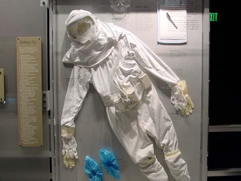
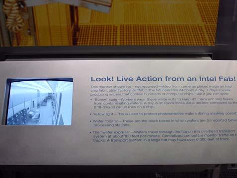
4 Forming the vertical structure: technology Forming the horizontal structure: design separated in space and time Their relationship is given by the Design rules referring to the technology. 9/16/02 10/37 Fabricating VLSI circuits: the planar technology Planar: refers to the fact that all the circuits are fabricated in a plane Base: the silicon single crystal, fabricated in bars. The 2-12 diameter large, about 0.25 mm thick wafers are sliced from these. On one wafer several thousands of IC chips or dies are fabricated at the same time Finished wafers before dicing 9/16/02 11/37 The group of wafers processed together: a party A party is being put into a furnace Very high cleanness requirements: clean rooms 9/16/02 12/37


5 9/16/02 13/37 9/16/02 14/37 9/16/02 15/37


6 9/16/02 16/37 9/16/02 17/37 9/16/02 18/37

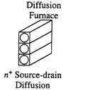
7 9/16/02 19/37 Microelectronics fabrication process A sequence of doping, deposition lithographic process steps 9/16/02 20/37 Doping procedures: aims at changing the doping at certain volumes of the semiconductor methods: diffusion ion implantation Diffusion: as a result of the elevated temperature (about.1000 C ) the dopant atoms from the ambient diffuse into the silicon at the locations where this is not prevented by SiO 2. The silicon dioxide masks against the diffusion. 9/16/02 21/37
8 Doping profile after diffusion x = 0 is the surface, x points perpendicularly inwards the Si The doping of the surface layers is stronger Side diffusion has to be considered 9/16/02 22/37 Ion implantation: shooting accelerated ions into the Si Doping profile after ion implantation x = 0 is the surface, x points perpendicularly inwards the Si 9/16/02 23/37 Advantages of ion-implantation over the diffusion higher accuracy, low temperature operation no size difference between the mask and the doped surface area disadvantages: damaged crystal structure less productive than diffusion 9/16/02 24/37
 2.")
9 Layer deposition steps Chemical or physical methods to produce contiguous layer on the surface Oxidation Production of SiO 2 layer on the surface of Si in oxygen ambience at about 1000 C temperature. The SiO 2 layer on the surface is perfect conductor, behaving selectively against chemicals The double role of SiO 2 1. Fabrication technological (masks) 2. Electronic insulation between the surface layers (Thick oxide) dielectric of MOS transistors (thin oxide) 9/16/02 25/37 Epitaxial layer deposition Forming of a Si layer on the surface that continues the single crystal structure, but e.g. with lower doping density 1200 C temp.process. CVD (Chemical Vapor Deposition) deposition of amorphous or polycrystalline Si onto the surface PVD (Physical Vapor Deposition) For the deposition of metal layers (evaporation or sputtering ) 9/16/02 26/37 Steps of the lithography To form the patterning in the SiO 2 Steps photoresist deposition on the surface patterning oxide etching Chip patterns: reticle, wafer patterns masks. Photo-technical steps Illumination through the masks The mask patterns imaged into the SiO 2 New masks for all the technological steps a technology is defined by a series of masks Pattern data are produced by CAD programs 9/16/02 27/37
10 Possibilities for wafer patterning 9/16/02 28/37 Photo-lithographic steps Patterning the SiO 2 mask Si-dioxide resist Si substrate At the illuminated areas the photo-resist polymerises, becomes resistive against certain chemicals, so that the mask pattern may be transmitted into the resist, later into the SiO 2 Si-dioxide Si After development 9/16/02 29/37 Si substrate After oxide etching: Si substrate After cleaning: Doping (e.g.diffusion) Si substrate The SiO 2 pattern masks against the diffusion 9/16/02 30/37


11 Individual steps Wafer operations are group operations cheap. Individual operations are expensive, should be minimised. Most of the testing steps have to be carried out on the wafer, the bad chips must not be packaged Dicing 9/16/02 31/37 Packaging The most frequent packaging methods Wire bonded flip chip 9/16/02 32/37 MOS IC fabrication steps The structure: p - oxide n + n + p + field implant Source/drain doping Layout: Thin oxide poli-si gate Metal contact W L 9/16/02 33/37


12 9/16/02 34/37 9/16/02 35/37 9/16/02 36/37

13 Example: detail of a fabricated IC, electron-microscopic image 9/16/02 37/37