Searching for new API Polymorphs Crystal Structure Determination of Pharmaceutical crystals using Electron Diffraction Tomography
|
|
|
- Dina Francis
- 5 years ago
- Views:
Transcription
1 Searching for new API Polymorphs Crystal Structure Determination of Pharmaceutical crystals using Electron Diffraction Tomography Dr. Partha Pratim Das Application Specialist NanoMEGAS SPRL, Belgium

2 This document was presented at PPXRD - Pharmaceutical Powder X-ray Diffraction Symposium Sponsored by The International Centre for Diffraction Data This presentation is provided by the International Centre for Diffraction Data in cooperation with the authors and presenters of the PPXRD symposia for the express purpose of educating the scientific community. All copyrights for the presentation are retained by the original authors. The ICDD has received permission from the authors to post this material on our website and make the material available for viewing. Usage is restricted for the purposes of education and scientific research. PPXRD Website ICDD Website -
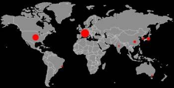
3 130 installations world-wide in TEM (26 countries)


TEM, EELS,")


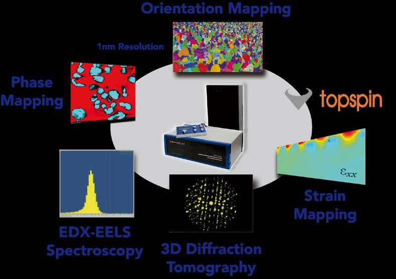
4 Free transnational access to the most advanced TEM equipment and skilled operators for HR(S)TEM, EELS, EDX, Tomography, Holography and various in-situ state-of-the-art experiments SME participation NanoMEGAS CEOS
5 Searching for API Polymorphs and solving their nanostructure by TEM Electron Diffraction

6 STRUCTURE ANALYSIS WITH ELECTRON DIFFRACTION Why electrons? times stronger interaction with matter compared with X-ray single crystal data on powder sample short data collection time - X- Ray peaks broaden with crystals of nm range With Electron microscope we can study nm- and micro-sized crystals
 Diffraction selected area, nano- and")
 Chemical")
7 STRUCTURE ANALYSIS WITH TEM Transmission electron microscopy (TEM) Diffraction selected area, nano- and convergent beam electron diffraction Imaging conventional, high resolution (HREM) Chemical analysis EDS and EELS

 Point resolution (Å)")

8 STRUCTURE ANALYSIS WITH TEM With TEM microscopes we can obtain images of crystalline materials with atomic resolution: Acceleration voltage (kv) Point resolution (Å) TEM grid 3.05 mm size 120 ~ We can see and analyze nano-crystals Very small quantity of sample!


 may produce ED")


9 STRUCTURE ANALYSIS WITH TEM TEM : Electron diffraction advantages TEM goniometer Diameter of grid mm Every TEM (electron microscope) may produce ED patterns and HREM from individual single nanocrystals ED information: Cell parameter and symmetry determination Measuring intensity values leads to structure determination
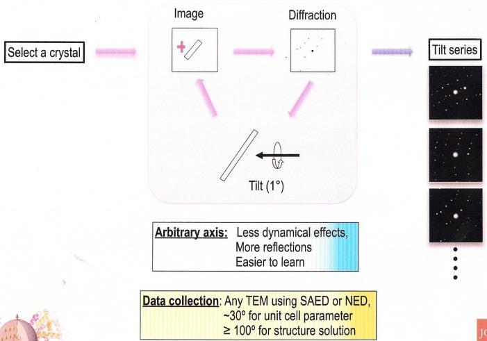
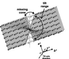


10 3D Diffraction tomography in TEM : 3D reconstruction of Reciprocal space TEM holder 50 nm 500 nm Kolb et al., Ultramicroscopy 107 (2007)
11 TEM - organic samples Cryo Cooling Can be used to Reduce beam damage Keeping Crystal deep Frozen Kolb et al, Polymer Reviews, 50: , 2010
12 TEM - organic samples What is the allowed maximum (critical) dose? Most biological specimens (proteins) 6 e-/å 2 Glaeser, 1971 Aromatic polymers (such as polystyrene) 36 e-/ Å 2 Anthracence 42 e-/ Å 2 Poly-xylene 120 e-/ Å 2 Kumar & Adams, 1990; Williams & Carter, 2004 Zeolites 100 e-/å 2 Ceramics 600 e-/å 2 Pan & Crozier, 1993
.")
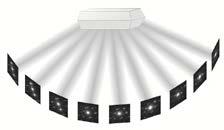
13 STRATEGY 1: FAST TOMOGRAPHY APPROACH Crystal is continuously rotated during sequential pattern acquisition avoiding intermediate stops for relocation of the crystal The missing wedge of the reciprocal space between the patterns is recorded by longer exposures during the crystal tilt Data Collection data can be recued <15 mint Gemmi et al. J. Appl. Cryst. (2015). 48
14 STRATEGY 2: FAST TOMOGRAPHY + Direct Electron Detection Camera Ideal detector for low intensity TEM Less radiation damage on sample gives more information For instance: more rotation information Very sharp images (No blurring effects from electron multiplication as in CCD) Medipix-Timepix 1 Electron TimePix = CMOS 1 Count x 100 more 512 x 512 pixels (262k pixels) sensitive than CCD > 120 fps X 10 more sensitive than IP dynamic range is (13 bit) per frame 55 micron pixel 25 μs exposure Acta Cryst. (2016). A72,

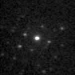
15 Low dose with Timepix < e-/ Å 2 /sec High Resolution Diffraction Pattern without Cryo
 crystal (Data collected -25 0 to 26")
.")
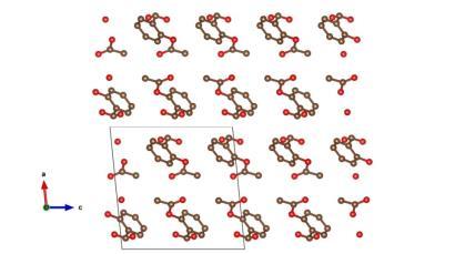
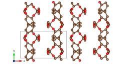
16 Data Collection with Fast Tomography + Timepix- CMOS of carbamazepine (CBZ) crystal (Data collected to 26 0 ) 55 frames summed / 1 0 NO CRYO USED Resolution: 0.8 Å Collection time < 3 min Acta Cryst. (2016). A72,


17 Ab-initio structure solution of carbamazepine (CBZ) crystal from ED Data Experimental a = 7.68 Å b = Å c = Å β = ο NO CRYO USED Literature Reported a = Å b = Å c = Å β = 92.94Å


 NO CRYO")
18 Data Collection with Timepix-CMOS Nicotinic Acid Crystal Resolution: 0.8 Å (Data collected to 26 0 ) NO CRYO USED Collection time < 3 min

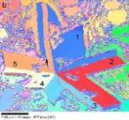
.")
19 Structure was solved ab-initio by DM from ED Data Solved from ED Literature Reported Unit cell from ED a = 7.19 Å b = Å c = 7.28 Å β = Literature Reported a = 7.19 Å b = Å c = 7.23 Å β = Å Acta Cryst. (2016). A72,

20 Acta A72 (2016) doi: /s
 doi:10.")
21 Acta A72 (2016) doi: /s CBZ Nicotinic Acid Nicotinic Acid
22
 a = 4.")

 Å b = 12.")
 Å SPG: P2 1 2 1 2")
23 API 1 (ED Obtained Unit Cell and SPG) a = 4.99 Å b = Å c = Å SPG: P (Obtained by X-ray) a = (4) Å b = (11) Å c = (2) Å SPG: P Collaboration TeraCrystal
24 Structure Solution Using ED Data API 1
 RED- Structure from Electron Diffraction (SA) Collaboration")
25 API 1 Comparison with x-ray structure Blue Structure from SCXRD (Direct Methods) RED- Structure from Electron Diffraction (SA) Collaboration TeraCrystal
 a = 7.56 Å b = 38.07 Å c = 8.")

 Å c = 8.5629(12) Å β = 108.")
26 API 2 (ED Obtained Unit Cell and SPG) a = 7.56 Å b = Å c = 8.61 Å β = ο SPG: P2 1 /n (Obtained by X-ray) a = 7.627(1) Å b = (4) Å c = (12) Å β = (15) ο SPG: P2 1 /n Collaboration TeraCrystal


 In Collaboration with")
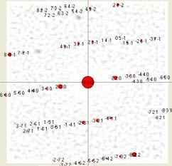
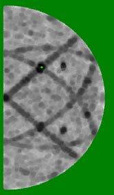
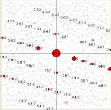
27 STRATEGY 3: Random Tomography Collection of 12 random quasi- oriented PED patterns at 300 kv spot size 10 nm scanning at high speed rates > 50 fps CRYSTAL UNIT CELL is calculated from several random patterns (oriented or not) In Collaboration with University of Cambridge, UK

28 131 ZA ZA ZA 512 ZA 023 ZA ZA ZA 001 ZA EDIff software : cell parameters are found from 11 random PED patterns a b c alpha beta gamma


29 Validation of Result ASPIRIN form I (: a=11.233(3) Å, b=6.544(1) Å, c=11.231(3) Å, â = 95.89(2)


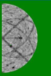
30 ZA close to [110] ZA close to [-1-1-5]
31 Nanoscale Texture Studies Crystalline and Amorphous Phase Mapping Using TEM Electron Diffraction


32 TEM Orientation imaging /phase mapping characterization at 1 nm scale (EBSD-TEM) from nm EBSD-SEM to 1 nm EBSD -like TEM 10 nm


 5-10")
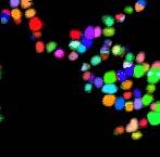
33 ASTAR : Crystal Orientation Mapping & Phase mapping at nanoscale Scan sample area 1 µm Orientation map Scanning the TEM beam in precession mode Step size 0.1 nm -100 nm Dedicated CCD with > 100 frames /sec Typical area 5 x 5 microns Scanning times (typical) 5-10 min Orientation map

")


34 Identification example : nanocrystalline Cu Diffraction pattern ( nanocrystalline cubic copper) correlation index = 585 Correlation index map For a given ED pattern, the correlation index map is calculated for all possible template orientations and plotted on a map that represents a portion of the stereographic projection (reduced to a double standard triangle). That resulting map reveals the most probable orientation for every experimental spot ED pattern ( in this case ED pattern is found to be close to 110 ZA orientation )

35 TEM orientation imaging : Spatial Resolution 1 nm to 500 nm Cu grains of different sizes Courtesy Muriel Veron Grenoble INP


36 Hydroxyapatite young bone Red: 001 Green:100 Blue: 010 Apatite nanocrystals of different sizes and orientations Courtesy Dr. R. Kroger, Univ of York


37 TEM : visualize EXACT amorphous / nanocrystalline content in a sample Example : Mg-Cu-Gd partly recrystallized metallic glass with Mg 2 Cu and Cu 2 Gd crystalline precipitates Crystalline or Amorphous? amorphous crystalline
38 CONCLUSIONS Most important reasons to use Electron Diffraction Nanocrystalline samples that give poor X-Ray patterns Inconclusive cell determination /crystal structure from X-Ray Detailed overview over crystalline vs amorphous content Solve crystal structures ab-intio from 50 nm-micron size crystals How Electron Diffraction can be used? Use any TEM (120, 200, 300 kv LaB6 or FEG) 3D precession diffraction tomography (ADT-3D) can help to find ab-initio the unit cell / crystal structure of any unknown crystal < 50 nm Random precession diffraction tomography (ASTAR) to find unit cell and crystal structure by reconstructing reciprocal space from quasi-oriented PED patterns Reveal detailed local amorphous vs crystalline part in samples
39 COLLABORATIONS University of Valencia, Spain University of Basel, Switzerland University of Cambridge, UK Center for Nanotechnology Italy SIMAP-INP Grenoble-France, Dr. Edgar Rauch Amsterdam Scientific Instruments/Teracrystal CONTACT US