Semiconductors. The essential materials for microelectronics technology A key property: conductivity (or resistivity) - large dynamic range
|
|
|
- Stephen Powell
- 5 years ago
- Views:
Transcription
1 Semiconductors The essential materials for microelectronics technology A key property: conductivity (or resistivity) - large dynamic range - controllable (or engineerable)
2 Example of controllable conductivity CE: large resistance CE: small resistance
3 Materials for semiconductors Crystalline Amorphous Inorganics Organics Materials DON'T define semiconductor: they are embodiments of the semiconductor concept Semiconductor is NOT defined by the materials: it is defined by the electrical properties: neither insulator nor conductor (later on, we will see a fundamental property is a band gap)


4 Crystal structure demos When atoms are arranged regularly (crystalline) When atoms are arranged randomly (amorphous)

5 Common semiconductors II III IV V VI B C N O Mg Al Si P S Zn Ga Ge As Se Cd In Sn Sb Te Hg Tl Pb II-VI III-V IV IV-VI ZnS ZnSe CdTe ionic GaN, AlN GaAs InP InSb C Si Ge covalent PbS PbSe PbTe
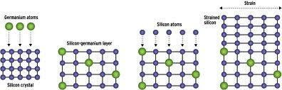
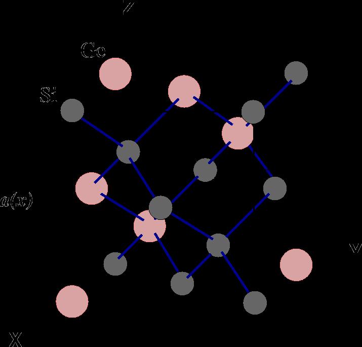

6 Stoichiometrically alloyed semiconductors Si-Ge

7 Stoichiometrically alloyed semiconductors III-V Ga As Ga x In 1-x As Ga In As x 1-x y P 1-y
8 Crystalline Amorphous Crystalline Polycrystalline

9 Hologram of Si crystal

10 Electron bonding in a crystal


11 Some crystals Diamond or Si AlN/GaN See links to wolfram demonstrations

12 Analysis of crystal structure

13 Construction of a crystal (see HW)
14 Key concepts of crystal structure Periodic: if you know a basic structure, you know the rest of the crystal The unit of one period is called unit cell If we know one unit cell, we should be able to describe the rest of the crystal! How? T lmn la mb nc Translation vector Unit vectors r r T lmn Integer
15 Crystal plane Miller index: a way to label a plane Take inverse Multiply the least common denominator Miller index z x 2 y All parallel planes have the same index
16 Crystal structure affects electron transport
17 Common semiconductor bandgap vs. lattice constant
18 Impurities in semiconductors materials that are not part of that particular semiconductor: examples: a very small amount of Si atoms in a GaAs crystal. The Si atoms are impurities (even though Si crystal is a semiconductor) Why do impurities matter? impurities affect the transport properties of a semiconductor. It can make the semiconductor negative type (n-type) or positive type (p-type). It can make semiconductor highly conducting (shallow donors or acceptors) or highly insulating (deep traps). We want to have total control of a semiconductor transport properties so that we can engineer devices; uncontrolled impurities limit our ability to engineer the devices, therefore, uncontrolled impurities are not desirable.
19 - But: controllable impurities are desirable because this is how we make devices. - Controlled insertion of impurity is call doping. Such a SC is called a doped semiconductor What is p-doped and what is n-doped? - Sometimes, as a part of the crystal growth process, some impurities are incorporated unintentionally, but they have a strong consequence and must be taken into account in the engineering of devices, this situation is called unintentional doping Eliminating uncontrolled impurities or unintentional doping has been the top priority in the crystal growth business for a long time. Now a day, the level of purity of commercial SC is reaching an ultra low level: better than 1 part in ; where it hardly matters in many cases.
20 Defects Defects are locations within a crystal where the structure deviates substantially from the ideal crystal structure. Common types of defects: point defect, line dislocation, twinning.
21 Point defects Schottky Frankel
22 Dislocation defects Line dislocation: edge dislocation Screw dislocation
23 Twinning defects
24 Twinning in Si

25 Stacking fault
26 Why care about defects? Defects are mostly undesirable (to the best of my knowledge): they always make devices worse, and they virtually have no use in device engineering except for very minor roles in some cases (defects are intentionally induced sometime by ion bombardment to cause a part of semiconductors to be non-conducting or light-absorbing, for example in laser fabrication). Defects can cause deep traps, slow down carriers, shortened carrier lifetime, and can lead to catastrophic failures or degradation of devices. (The diode laser was invented in 1964, but it took over 15 years to turn it into a ubiquitous product, because early devices were very short-lived, because of material defects. Elimination of defects was the crucial step in giving us today communication, CD players, laser printers, ) A big part of crystal growth business is to grow crystals with lowest defect densities.
27 Crystal growth technology (assignment 1) The drive in making big single crystal is the economic of chip fabrication: bigger wafer results in lower production cost per chip. Epitaxial growth: the veneer analogue of semiconductor: most of the time, devices are fabricated on a thin layer (microns) near the surface. It is necessary to have good crystal only within this layer. People came up with the idea of growing just a thin layer of high quality crystal on top of another, called substrate. Crystal bonding: another technique: two crystals are bonded along their surface at the molecular level.
28 Bulk Crystal Growth cyj_vqcyi78 klw8j1c-1lk 8T5xWQ0nC_8
29 Epitaxial Growth NsGRKSV8yH8 zner-jf8958
30 Elements of semiconductor physics The roads Materials: crystals, defects Electronics structure Impurities Electrons, holes The cars The drivers