Metallizing High Aspect Ratio TSVs For MEMS Challenges and Capabilities. Vincent Mevellec, PhD
|
|
|
- Katrina Evans
- 5 years ago
- Views:
Transcription

1 Metallizing High Aspect Ratio TSVs For MEMS Challenges and Capabilities Vincent Mevellec, PhD
2 Agenda Introduction MEMS and sensors market TSV integration schemes Process flows for TSV Metallization aveni technologies and mechanisms Conclusion 2

3 aveni Introduction -Who Are We? aveni develops disruptive wet deposition technologies for 3D TSV and 2D interconnects Our technology creates superior quality films for isolation, barrier, seed, and fill applications High aspect ratios for TSV (vs. 10:1, the current industry standard); achieved 40:1 Key for MEMS of tomorrow, IoT, automotive, and biotechnology applications Headquartered in France, with service offices worldwide: Silicon Valley, Taiwan, Korea, et. al. 3


 Source: 3DInCites.")
4 Through Silicon Via (TSV) Introduction TSVs have been in existence for over 20 years First patented by Shockley in 1962 Most commonly used in CMOS image sensors TSVs offer several advantages over flip-chip stacking or wire bonding Higher interconnect density shortens signal path for faster operation at lower power Better utilization of chip real estate Devices with enhanced performance, integration, and smaller form factor TSVs have carved out a niche in advanced heterogeneous semiconductors Graphics chips integrating high bandwidth memory with graphics processing units on interposer (2.5D integration) Source: 3DInCites.com, Fraunhofer, et. al. Source: AMD 4

5 MEMS and Sensors Market 12% CAGR expected for MEMS and sensors revenue $38B in 2016 to $66B in 2021 MEMS segment of the market is 30%, with expected 14% CAGR through

6 MEMS Market by Device MEMS device market is quite broad TSVs and related technology used in a subset of devices aveni served markets 6

: 20:1; 5 x 100 µm")


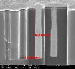
7 Via First TSV Integration Defines TSVs Before CMOS Via First TSV Via First (Polysilicon fill) Aspect Ratio (AR): 20:1; 5 x 100 µm Trench Poly filled vias and trenches are used for electrical connections in MEMS components that can withstand high temperature Courtesy CEA-Leti 7


8 Via Middle: TSVs Formed After FEOL CMOS, Before BEOL Via Middle TSV Via Middle (Copper fill) AR: 7:1 8:1 9:1 10:1 Size: 2 x 15 μm 10 x 80 μm 6 x 55 μm 10 x 100 μm TSV Cu fill is compatible with Via Middle Courtesy CEA-Leti 8


9 Via Last: TSVs are Formed After BEOL and Wafer Bonding Via Last TSV Via Last (Copper seed) Aspect Ratio: 1:1 2:1 3:1 Via Size: 80 x 80 μm 60 x 120 μm 40 x 120 μm Via Last has limited thermal budget (< 250 C) Generally large vias with low aspect ratio (<5:1), common with CIS Thick conformal copper to allow electrical contact Courtesy CEA-Leti 9
10 TSV Metallization Challenges at High Aspect Ratios (HAR) Layer Barrier Seed Fill (Plating) Requirements Conformal deposition with continuous coverage Low temperature deposition (Via Last) Low resistance Conformal deposition Continuous layer on sidewalls (no breaks) Minimize overburden Void-free deposition within entire TSV HAR TSVs HAR is generally defined to be 10:1 (height / width) 10
11 Process Flow Variations For TSV Metallization Layer Insulator Metal Barrier Cu Seed Deposition Process Type Dry PE-CVD SA-CVD ipvd CVD ALD ipvd CVD Wet in development Electroless (ELD) Chemicalgrafting (cg ) 1 Electrografting (eg ) 2 Dry deposition processes are challenging to integrate as aspect ratio increases >8:1 Integrating wet Cu seed meets technical needs for high aspect ratio TSVs Cu Fill 1 aveni Neso electroless deposition 2 aveni Rhea CVD Electrochemical Deposition (ECD) 11


12 Conventional Dry Techniques for TSV Metallization Physical vapor deposition (PVD) Plasma Enhanced Chemical Vapor Deposition Atomic Layer Deposition Courtesy Dow Corning, Oxford Instruments 12
 is usually preferred for its improved step coverage vs.")

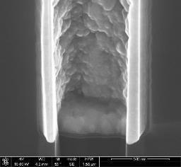
 8:1 AR - Void-free filling Increasing AR >10:1 AR - Voiding from seed discontinuity PVD")
13 ipvd Seed Layer ipvd Barrier Barrier and Seed Layers are Commonly Deposited Using PVD Ionized Physical Vapor Deposition (ipvd) is usually preferred for its improved step coverage vs. PVD ipvd TiN Barrier (10x80 µm) Barrier Location Thickness (nm) Field 750 % Step Coverage Upper 1/ Mid 43 6 Lower 1/ Bottom PVD Capabilities Reference / established process Compatible with all TSV integration types New materials available (seedless) 8:1 AR - Void-free filling Increasing AR >10:1 AR - Voiding from seed discontinuity PVD Limitations Low step coverage Low throughput at low temperature deposition (Via Last) Higher cost of ownership Courtesy CEA-Leti 13
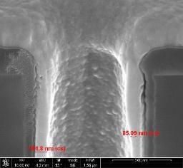
 Barrier Location Thickness (nm) Field 56 % Step Coverage Upper 1/3 83 148 Mid 69 123 Bottom 33 59 MOCVD Capabilities Good step")

14 MOCVD TiN (20:1) MOCVD TiN (8:1) Metal-Organic Chemical Vapor Deposition (MOCVD) Barrier For HAR barrier deposition, MOCVD appears the most promising option Precursor available for 200 C for Via Last compatibility MOCVD TiN Barrier (8:1 TSV) Barrier Location Thickness (nm) Field 56 % Step Coverage Upper 1/ Mid Bottom MOCVD Capabilities Good step coverage Low temperature deposition Extendibility up to 15:1 AR Controlled process for barrier layer MOCVD TiN Barrier in 10 x 200 μm TSV Barrier Location Thickness (nm) Field 67 % Step Coverage Upper 1/ Lower 1/ Bottom MOCVD Limitations Industrial scale integration to be confirmed Hardware development required for copper seed Courtesy CEA-Leti 14

15 ALD Barrier Atomic Layer Deposition (ALD) For Barrier ALD processes are becoming more mature for BEOL, but they have some limitations for TSV applications Extremely stringent requirements for chemical injection system and chamber design Step coverage in deep trench structures is a function of precursor residence time Long cycles and high pressure are required to minimize defect formation ALD Capabilities High conformality in high aspect ratio features Stoichiometry control Low defect density ALD Limitations Requires high temperature deposition; limits integration options Very slow / low throughput process (long pulse period) Thimsen, E. et al. Chem Mater 24, (2012) 15

")
 Compatible with all")

 Requires")
16 Neso Results Electroless Mechanism Cu Diffusion Barrier Layer With E-less Deposition Electroless Capabilities Ultra conformal (100% step coverage) Low resistivity (no copper seed required) Compatible with all insulator substrates 40:1 Aspect Ratio Electroless Limitations Organic activation One shot activation (1 hour stability after mixing) Requires dedicated equipment 16

 Adhesion to be improved on")
17 Neso Results Electroless Mechanism Cu Diffusion Barrier Electroless Deposition On Polysilicon Electroless Capabilities Aqueous-based activation Adhesion improvement Batch activation capability (single or multi wafer) Electroless Limitations NiB Ni2Si p-si SiO2 Requires additional processing step (poly-si) Adhesion to be improved on amorphous Si 17
18 Electrografted (eg) Rhea Cu Seed Layer Mechanism Strong adsorption on barrier layer High adhesion High nucleation density Reduced terminal effect Electrochemical reduction Metal barrier (Dry or Wet) Complexing agent Copper ions Cu Cu deposition 18
 Rs = 37.")

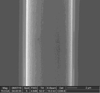
19 Wet Cu Seed Layer Maintains Barrier 300 mm 70 nm MOCVD TiN 70 nm MOCVD TiN nm Rhea Cu seed (as deposited) Rs = Ω/sq Non-unif = 4.12% 1 σ Rs = Ω/sq Non-unif = 3.86% 1 σ aveni Rhea Cu Seed from 300 mm Semitool Raider ECD-312 wet deposition system 19
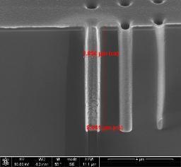
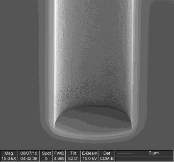
 10:1 (5x50µm) 20:1 (5x100µm) 35:1 (0.25x7µm) Aspect Ratio PVD (Dry) Cu Seed 1 μm Cu Seed Si Rhea Wet Cu Seed 0.")
20 Step Coverage TSV Cu Seed Step Coverage Benchmarking Study 100% 80% 60% 40% 20% 0% Step coverage vs. Aspect Ratio for Dry and Wet Cu Seed 5:1 (5x25µm) 10:1 (5x50µm) 20:1 (5x100µm) 35:1 (0.25x7µm) Aspect Ratio PVD (Dry) Cu Seed 1 μm Cu Seed Si Rhea Wet Cu Seed 0.2 μm Cu Seed Si PVD (Dry) Rhea (Wet) Pad Pad aveni Rhea solution requires less CMP processing vs. PVD seed 20


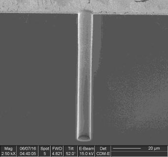
21 Wet Cu Seed with Dry TiN Barrier and Conventional ECD Filling Rhea Cu Seed in 10 x 100µm TSVs Rhea + ECD after annealing (wafer center) Highly conformal Rhea Cu Seed deposited in 10 x 100 mtsvs enables void-free filling at 300 mm Courtesy CEA-Leti 21


22 Kelvin and TSV Daisy Chain Yield Curves CVD TiN-Rhea Gen III PVD TiN-Rhea Gen IV Rhea repair CVD TiN- Rhea Gen III PVD TiN- Rhea Gen IV Rhea seed layer 10 x 100 µm Kelvin 10 x 100 µm 754 TSV Daisy Chain 100% yield in 10 x 100 μm TSV with Rhea Cu seed layer Courtesy CEA-Leti 22
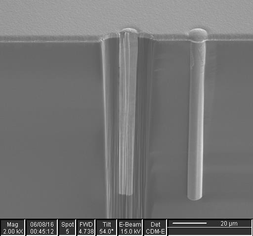
23 Extendibility to Narrow Diameter and High Aspect Ratio TSVs Full via Top Mid 0.8 x 9 μm (9:1) TSV Rhea Cu seed layer deposition Post copper plating 10 x 120 μm (12:1) TSV Full via Mid Bot Courtesy CEA-Leti 23

24 Final Product with Via-Last Integration Work ongoing with Teledyne DALSA and Freescale (NXP) at C2MI (Bromont, Canada) Final devices successfully connected by TSVs at wafer scale using Rhea seed layer Courtesy of 24
25 Conclusions As the demand for smaller MEMS devices increases, so will the need for HAR TSVs Integration scheme choice for TSV depends on device type, desired properties, and primarily thermal budget considerations Limitations for TSV dry processes (barrier and seed layers) arise for aspect ratios >8:1 Wet Cu seed is compatible with conventional plating tools High step coverage and reduced CMP process time with wet Cu seed Extendible to narrow TSV diameters ( 5 µm) and high aspect ratios ( 10:1 AR) 25
26 Acknowledgements Part of this work was partly funded thanks to the French national program Programme d Investissements d Avenir, IRT Nanoelec ANR-10-AIRT

27 THANK YOU