Czochralski Crystal Growth
|
|
|
- Lucas Warren
- 5 years ago
- Views:
Transcription
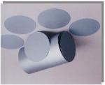
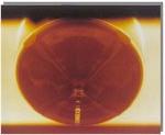
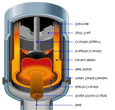
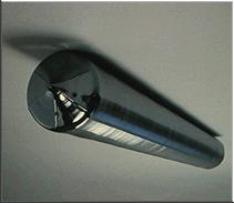
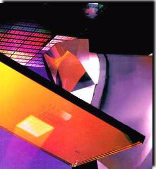
1 Czochralski Crystal Growth Crystal Pulling Crystal Ingots Shaping and Polishing 300 mm wafer 1
2 2
3 Advantage of larger diameter wafers Wafer area larger Chip area larger 3
4 4


5 Large-Diameter Wafer Handling La Vals Fab Production Fab 300mm wafer vs pizza Overhead rail transport of wafer cassette Lateral uniformity of processing effects across the WHOLE wafer is key consideration for microfabrication design 5
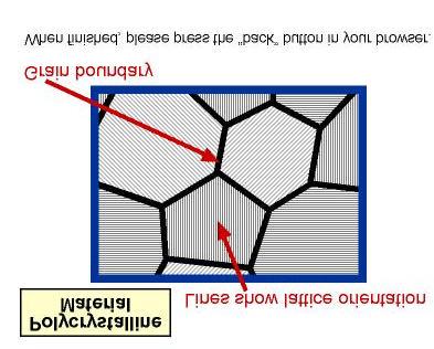
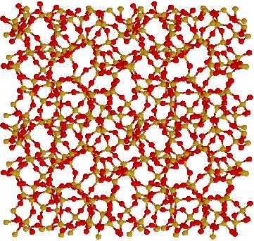
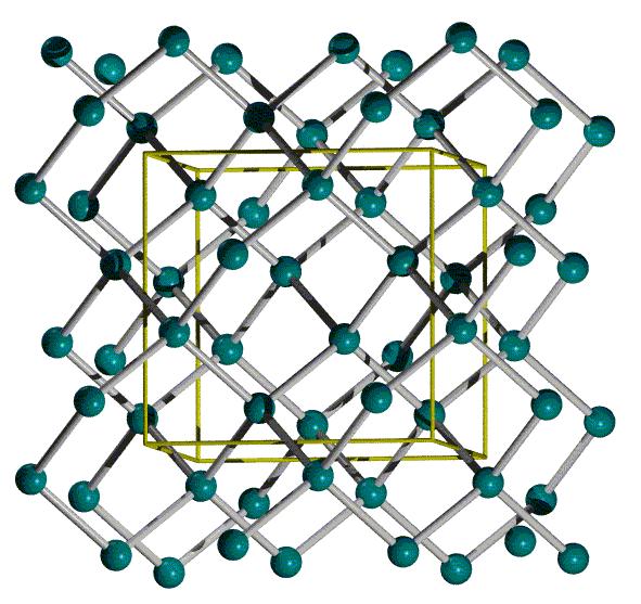
6 Microstructure of Electronic Materials Amorphous materials Single-Crystal Material 6

7 Photolithography glass plate chromium Positive Resist Part exposed to light will be dissolved in development solution. Processing Temperature Ambient 7
8 The Photo-Lithographic Process oxidation optical mask photoresist removal (ashing) photoresist coating photoresist exposure process step spin, rinse, dry acid etch photoresist develop
 Isotropic (e.g. Wet Etching) 9")
9 Etching Pattern resist mask Etching thin film Etching completed Remove resist mask Processing Temperature Ambient Anisotropic (e.g. Reactive Ion Etching) Isotropic (e.g. Wet Etching) 9
10 Etching Selectivity Example: HF solution etches SiO 2 but not Si SiO 2 HF solution Si Si * A high etching selectivity is usually desired 10
 Si substrate Etching continues Etching stops Effect of different mask")
11 Anisotropic Wet Etching of Si Crystals Etchants : KOH or EDP (Ethylene-Diamine_Pyrocatechol) Top view Cross-section (100) Si substrate Etching continues Etching stops Effect of different mask opening 11
 - use O 2. Dry oxidation Thick oxide growth (e.g. field oxide) - use H 2 O.")
12 Thermal Oxidation Processing Temperature o C Si + O 2 SiO 2 Si + 2 H 2 O SiO 2 + 2H 2 Oxide (X ox ) thickness t t O 2 (or H 2 O) diffuses through SiO 2 and reacts with Si at the interface to form more SiO 2. 1µm of SiO 2 formed consumes 0.44 µm of Si substrate. Thin oxide growth (e.g. gate oxide) - use O 2. Dry oxidation Thick oxide growth (e.g. field oxide) - use H 2 O. Wet oxidation Oxidation time(t) 12
13 Uneven surface topography with window oxidation 1 st oxidation Si Realistic topography with 2-dimensional effect 2 nd oxidation SiO 2 Si Pattern oxide window by litho and etch SiO 2 SiO 2 SiO 2 Si Si Si Note uneven Si surface after window oxidation 13
14 Local Oxidation O 2 silicon nitride pad oxide ~100 A LOCOS Process Si SiO 2 Si 3 N 4 Thermal Oxidization nitride Si 14

15 Ion Implantation typically used to introduce dopans into semiconductors Ion Energy ~1 kev to 200 kev Processing Temperature Room temp during implantation. After implantation, a 900 o C-1000 o C anneal step is needed to: 1) activate dopants 2) restore Si crystallinity 15
![Diffusion To introduce dopants into semiconductors [ Predeposition] To spread out the dopant profile [ Drive-in] D D](/docs-images/90/103024591/images/16-0.jpg "Q T = = D 0 e Q kt Diffusion Constant = Activation = Temp in K Energy ( D as T ) Processing Temperature 950-1200 o C")
16 Diffusion To introduce dopants into semiconductors [ Predeposition] To spread out the dopant profile [ Drive-in] D D Q T = = D 0 e Q kt Diffusion Constant = Activation = Temp in K Energy ( D as T ) Processing Temperature o C 16
17 Predeposition Si surface concentration maintained at constant C s (solid-solubility) during predep. Dose of dopant incorporation = C 2 s π Dt 17
18 Predeposition and Drive-in Half-gaussian depth profile after long drive-in. Predep only Dopant dose conserved during drive-in. Diffusion distance Predep +Drive-in ( ) Dt Concentration versus Depth 18
19 Physical Vapor Deposition (1) Evaporation Deposition Si Substrate Substrate at ~ room temp Deposited Al film (polycrystalline) evaporation Al charge (T source >>T boiling of Al, 700 O C) 19
20 Physical Vapor Deposition (2) Sputtering Deposition Si Substrate Substrate at ~ room temp Deposited Al film (polycrystalline) Ar + Ar ions with ~ kev kinetic energy Al target Al atoms ejected due to Ar ion bombardment 20
21 Chemical Vapor Deposition (CVD) Processing Temperature o C 21
22 Epitaxial Growth Processing Temperature o C Requires an ultra-clean Si surface prior to epi growth. Requires deposition of Si at very high temperature for perfect crystallinity. 22
23 Epitaxial Growth <Si> substrate 1) In-situ surface cleaning 2) Si CVD at high temperature <Si> Epi layer <Si> substrate Typically used when we need a lightly doped singlecrystal Si layer on top of heavily doped substrate. Example n - <Si> /cm 3 n + <Si> e.g /cm 3 23


24 Cost of Silicon Real Estate 200mm Si wafer 200mm Epi wafer 1812 sq/ft House Menlo Park, CA $80 $140 $944,492 $0.25 /cm 2 $ 0.44 /cm 2 $0.56 /cm 2 24
25 Chemical Mechanical Polishing (CMP) Wafer is polished using a slurry containing silica abrasives (10-90 nm particle size) etching agents (e.g. dilute HF) Backing film provides elasticity between carrier and wafer Polishing pad made of polyurethane, with 1 µm perforations rough surface to hold slurry Ambient Temperature 25
 at high")
26 Rapid Thermal Annealing (RTA) Sub-micron MOSFETs need ultra-shallow junctions (x j <50 nm) Dopant diffusion during activation anneal must be minimized Short annealing time (<1 min.) at high temperature is required Ordinary furnaces (e.g. used for thermal oxidation and CVD) heat and cool wafers at a slow rate (<50 o C per minute) Special annealing tools have been developed to enable much faster temperature ramping, and precise control of annealing time ramp rates as fast as 200 o C/second anneal times as short as 0.5 second typically single-wafer process chamber:
 layers shallow trench isolation (STI) copper metallization Oxide Isolation of Transistors p+ n damascene process p+ SiO 2 p n+ p n+ IC with 5 layers of Al")
27 Chemical Mechanical Polishing (CMP) Chemical mechanical polishing is used to planarize the surface of a wafer at various steps in the process of fabricating an integrated circuit. interlevel dielectric (ILD) layers shallow trench isolation (STI) copper metallization Oxide Isolation of Transistors p+ n damascene process p+ SiO 2 p n+ p n+ IC with 5 layers of Al wiring

 (1) (2)")

28 Copper Metallization Dual Damascene Process (IBM Corporation) (1) (2) courtesy of Sung Gyu Pyo, Hynix Semiconductor (4) (3) (5)


29 Metal Plating ~ ambient temp 29
30 List of Conventional Microfabrication Modules Lithography Thermal Oxidation Etching (Chemical, Plasma) Ion Implantation Diffusion Physical Vapor Deposition PVD Chemical Vapor Deposition CVD and Epitaxial Growth Chemical Mechanical Polishing CMP Metal Plating 30
31 Processing Temperature and Material Failure Temperature Process Temperature in C Resist Exposure Resist Reflow Resist Spin-on Resist Bake Sputtering Deposition Evaporation Deposition Si Melting Point (1412C) CVD Ion Implantation Post Implantation Anneal Thermal Oxidation Al-Si Eutectic (560C) Dopant Diffusion Epi 31