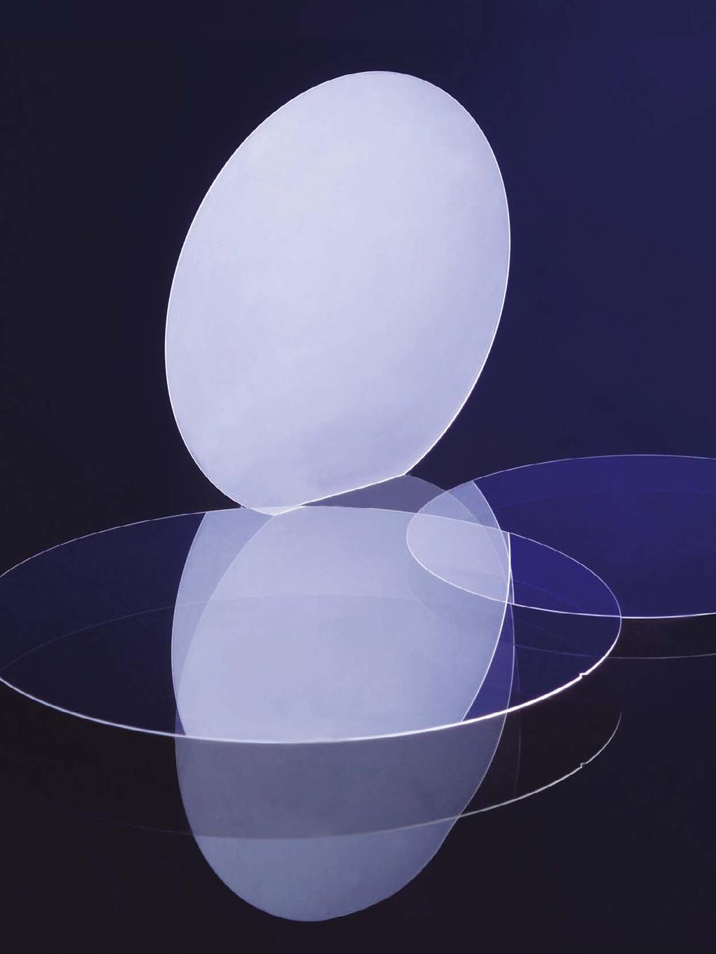
Glass Wafer. Specification
|
|
|
- Allan Ellis
- 5 years ago
- Views:
Transcription
1 Glass Wafer Specification
2 Glass Wafer Specification SCHOTT Thin Glass and Wafer products are the result of deep technological expertise. With a product portfolio of more than 100 optical glasses, special materials and wafer processing technologies, we are a valuable partner to customers worldwide in developing highly differentiated solutions for the semiconductor and biotech industry. This specification provides a full overview for our glass wafer manufacturing competencies. It describes our hot forming and processing capabilities we offer to the market. Due to the variety of customer requirements please feel free to contact our sales organization in order to discuss your requests in detail. Our sales is supported by application engineering in order to give customers needed support for best solutions. Beside this glass wafer specification SCHOTT has additional Datasheets for information about glass types and their physical and chemical properties as well for specific process or product related information. Please contact our sales for any needed support. Typical Applications AF 32 eco MEMpax / BOROFLOAT 33 FOTURAN II D 263 T eco / D 263 T B 270, B 270 i Wafer-Level Chip-Scale Packaging (WLCSP) Wafer-Level Optics (WLO) Thin Film Battery (TFB) Interposer Substrates Ultra-Thin Glass (UTG) Micro Electro-Mechanical Systems (MEMS) Microfluidics RF-MEMS-Sensors Microfluidics Micro-Optics IC Interposer IR-Cut Filter Touch Panel Microfluidics Lab-On-a-Chip Fingerprint Sensors Wafer-Level Chip-Scale Packaging (WLCSP) Optoelectronics Main Properties of Glass Wafers Excellent transmission Superior fire-polished surface finish for glass types Variety of available glass types matching your individual application needs Superior wafer flatness through state-of-the-art double side polishing processes Customized structuring Wide range of available thicknesses from mm up to 3 mm Outstanding dielectric properties (specific data available on request) Suitable solutions for different bonding technologies High quality processing following international industry s Customized properties available upon request (geometry, quality) 2
3 Glass Wafer from SCHOTT SCHOTT has several processes for wafer glass manufacturing and processing. This guide will present a brief overview of the glass wafer properties and their specific advantages: 1. Overview of glass types 4. Structuring capabilities 2. Glass formats & geometrical properties 5. Packaging methods 3. Wafer quality 6. Contacts 1. Overview of Glass Types SCHOTT offers a range of glass types produced in various hot forming technologies. The (DD) technology is the main process to produce glass wafers with superior surface quality directly out of the hot forming process without the need for any additional surface treatment (e.g. D 263 T eco, AF 32 eco). Our Up- (e.g. B 270 i) and Float (BOROFLOAT 33) production technologies are dedicated to materials where the customer applications may require additional surface treatment (lapping & polishing). Further details on physical and chemical properties of the above glass types are available in separate specifications of each glass type. Properties Optical Properties Units/ Condition D 263 T eco D 263 T Refractive index n D Luminous Transmittance τ vd65 (at thickness) % AF 32 eco MEMpax BOROFLOAT 33 B 270 B 270 i FOTURAN II (2 mm) (2 mm) Abbe value ν e Thermal Properties CTE α (20 C, 300 C) 10 6 K Transformation temperature Tg Mechanical Properties Density ρ *(annealed at 40 C/h) C g/cm³ 2.51* 2.43* 2.22* Young s modulus E kn/mm² Poisson s ratio μ Knoop hardness HK 0.1/ Chemical Properties Hydrolytic resistance acc. to ISO 719 Acid resistance acc. to DIN Alkali resistance acc. to DIN ISO 695 Electrical Properties Dielectric constant ε r Dissipation factor tan δ Class HGB 1 HGB 1 HGB 1 HGB 1 HGB 3 HGB 3 HGB 4 Class S 2 S 4 S 1 S 1 S 2 S 2 S 1 Class A 2 A 3 A 2 A 2 A 2 A 1 A 2 1 MHz 1 GHz 5 GHz 1 MHz 1 GHz 5 GHz
4 Additional properties Additional Properties D 263 T eco D 263 T AF 32 eco MEMpax BOROFLOAT 33 B 270 B 270 i FOTURAN II Hot Forming Technology Microfloat Ultra-thin glass possible ü ü ü ü Up- Alkaline content ü ü ü ü ü ü Anodic bonding with Si ü ü ü ü ü ü Electrostatic bonding ü ü ü ü ü ü ü Adhesive bonding ü ü ü ü ü ü ü Chemical toughening ü ü ü ü ü Wafer quality requests lapping & polishing ü ü ü 2. Glass Formats & Geometrical Properties Formats per glass types Upon request, SCHOTT also offers customized formats and shapes within the limits of production and processing capabilities, beyond those listed below. Sizes D 263 T eco D 263 T AF 32 eco MEMpax BOROFLOAT 33 B 270 B 270 i FOTURAN II Formats wafer min. max. 4 inch 4 inch 4 inch 8 inch Thickness range min. max mm 1.1 mm mm 1.1 mm 0.2 mm 0.7 mm 0.5 mm 3.0 mm 0.3 mm 0.9 mm 0.8 mm 3.0 mm 0.5 mm 3.0 mm Geometrical properties Property Thickness / Condition Specification / Tolerance Format tolerances depending on thickness ± 0.1 mm to ± 0.2 mm Thickness tolerances TTV Warp Roughness (Ra) Edge grinding (bevel width) Notch & Flat (SEMI ) 0.5 mm > 0.5 mm lapped & polished 0.5 mm 0.5 mm to 0.7 mm > 0.7 mm < 0.2 mm 0.2 mm to 0.5 mm > 0.5 mm lapped & polished 0.2 mm 0.7 mm > 0.7 mm < 0.2 mm 0.2 mm ± 5.0 μm ± 10.0 μm ± 20.0 μm 5.0 μm to 10.0 μm 10.0 μm 15.0 μm 300 μm to 2000 μm 80 μm to 200 μm 100 μm to 200 μm 0.5 nm 1.5 nm C- or Facet-shape 0.1 mm to 0.5 mm 0.1 mm to 0.7 mm flat only (cut only) flat and notch double flat and notch possible 4
5 3. Wafer Quality Quality Property Condition Specification Inspection condition cleaned uncleaned (cut glass only) Inspection time unaided eyes 15 seconds Inspection illumination Inspection procedure Visual properties Wafer cleaning Wafer quality level Edge quality (chips) Wafer laser marking (serial number possible) removing of removable particles < 5 10 μm scratch / dig MIL-PRF-13830B thickness 0.3 mm clean room at class 100 controlled room climate 1.5 klux to 180 klux distance 15 cm to 30 cm 100 % inspection clean room, cleaning machine supported by US/MS, DI-water 10/5 60/ μm to 300 μm Fonts: Arial, DOT, SEMI Size: 1 mm to 5 mm Reporting on request quality report for each shipment 4. Structuring Capabilities With our ultrasonic lapping (USSL) technology, SCHOTT has established a specific solution for structured glass wafers. Ultrasonic lapping requires a lapping and polishing surface treatment processing. Structuring Property Level USSL (Fig. 1) Thickness range Element shape Wafer size Element size Position & form element tolerance Pitch Edge to edge distance Angle shape position Taper angle 0.5 mm 0.4 mm round holes only 100 mm to 150 mm 200 mm 0.4 mm to 1.1 mm ± 80 μm ± 50 μm 1.75 mm 1.30 mm 1.20 mm 0.90 mm (90 ± 0.5) degree (90 ± 0.3) degree (90 0.5) degree Surface quality 10/5 40/20 Element quality (chips) 100 μm 50 μm Surface treatment requested lapping & polishing Fig. 1 Hole E Glass Thickness Ø D D: hole diameter E: angle shape position 5

 6 inch to spacer rings, Tyvek, plastic layer 6.")

6 5. Packaging Methods Depending on format and thickness we can offer various packaging methods. Basis are wafer boxes. Packing is done either inside or outside clean room. Clean room conditions: class 1000 including vacuum bags. Packing method Wafer Size Interlayer Picture Wafer box SCHOTT 4 inch to paper, Tyvek Wafer box SEMI 4 inch to 8 inch Cassette box (coin stack) 6 inch to spacer rings, Tyvek, plastic layer 6. Contacts Please feel free to contact us for any question related to our products or your projects. With a network of our Application Engineering which is situated worldwide we will find suitable solutions for your projects. SCHOTT North America, Inc. Advanced Optics 400 York Avenue Duryea, PA USA Phone / Fax / info.optics@us.schott.com 6