Major Fabrication Steps in MOS Process Flow
|
|
|
- Imogene McKenzie
- 5 years ago
- Views:
Transcription

 Photoresist Coating Mask-Wafer Alignment and")


 Polysilicon Deposition Polysilicon Mask and")


1 Major Fabrication Steps in MOS Process Flow UV light Mask oxygen Silicon dioxide photoresist exposed photoresist oxide Silicon substrate Oxidation (Field oxide) Photoresist Coating Mask-Wafer Alignment and Exposure Exposed Photoresist Photoresist Develop Ionized CF 4 gas photoresist oxide Ionized oxygen gas oxide oxygen gate oxide Dopant gas Silane gas polysilicon Ionized CCl 4 gas oxide Oxide Etch CF 4 or C 3 F 8 or CHF 3 O 3 CF4 +O 2 or CL 2 Photoresist Strip Oxidation (Gate oxide) Polysilicon Deposition Polysilicon Mask and Etch Scanning ion beam silicon nitride Contact holes Metal contacts ox S G D Ion Implantation top nitride G G S D S D S G D Active Regions Nitride Deposition Used with permission from Advanced Micro Devices Contact Etch drain G S D Metal Deposition and Etch
2 Lithography Basic concepts for photolithography, including process overview, critical dimension generations, light spectrum, resolution and process latitude. Difference between negative and positive lithography. Eight basic steps to photolithography. Wafer surface preparation for photolithography. Photoresist physical properties. Applications of conventional i-line photoresist. Deep UV resists Photoresist application techniques Soft bake processing
3 Model of Typical Wafer Flow in a Sub-Micron CMOS IC Fab Wafer Fabrication (front-end) Wafer Start Unpatterned Wafer Thin Films Polish Completed Wafer Diffusion Photo Etch Test/Sort Implant

4 Schematic creation of MOS field effect transistor. Gate electrode Source electrode Drain electrode Gate length Gate oxide
 through chemical vapor")
5 Step 0 The positively doped silicon wafer is first coated with an insulating layer of silicon dioxide (yellow) through chemical vapor deposition.
6 Step 1 An ultraviolet light-sensitive thin layer of photoresist (blue) is applied to the silicon dioxide surface and evenly spread across the wafer.
7 Step 2 The first mask is placed over the wafer and ultraviolet light is projected onto the mask. Areas of photoresist exposed to the light are hardened and those shielded remain soft. (Lithography step number 1)
8 Step 3 The unexposed (and soft) photoresist is removed by washing with a solvent, leaving the hardened resist and underlying silicon dioxide layer intact.
9 Eight Steps of Photolithography UV Light HMDS Resist Mask 1) Vapor prime 2) Spin coat 3) Soft bake 4) Alignment and Exposure 5) Post-exposure bake 6) Develop 7) Hard bake 8) Develop inspect

10 Lithography: 10 Step Process
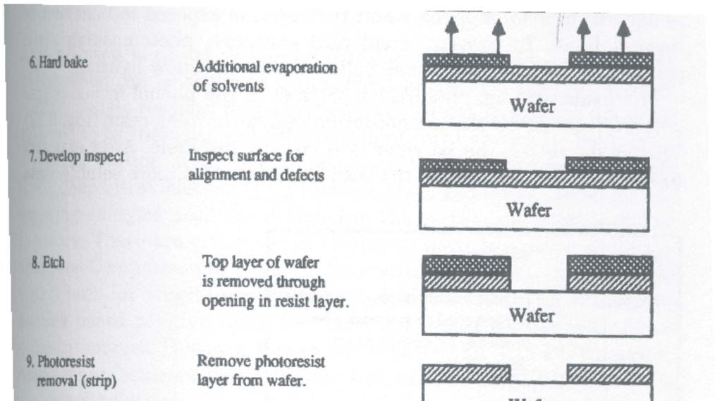
11 Lithography: 10 Step Process
12 Surface Preparation Surface preparation. Surface needs to be compatible with photoresist solvent and material. Want wetting of surface. Want boundary conditions for flow fixed at surface. Surface needs to be dry. Many resist material are hydrophobic and require dry surfaces for good adhesion Traditional solution is adhesion promoters chemicals that react with surface groups, especially ones that are hydrophilic, and convert to surface groups that are hydrophobic
13 Surface Drying Surface cleanliness is achieved by quick transfer of wafer from previous deposition (oxidation) step to this first lithographic step. If wafer had to be stored or transferred for an excessive amount of time, previously described cleaning steps have to be applied. (Spin-Rinse-Dryer) Wafer are stored in dry (<50% RH) air Particulate blow-off with hot nitrogen Three baking types possible: (low temp (150C), med. Temp (400C), high temp. (750C)). Low temp multilayer water is evaporated, Med. Temp monolayer water is evaporated, High Temp. surface OH groups are removed. Usually only low temp heating (easy).
14 Surface treatment procedures. HMDS in xylene(10-100%): common adhesion promotion agent. Hexamethyl disilazane (Me = CH 3 ) Reactivity toward surface hydroxyl groups 2 Surface-OH + HMDS 2 Surface-O-Si(Me) 3 + NH 3 Surface-OH: hydrophilic Surface-O-Si(Me) 3 : hydrophobic and oleophilic Web site with list of common surface preparation chemicals:


15 Influence of HMDS treatment on surface properties of Silicon.
16 Other Primers Trichlorosilane H 3 C CH 2 H 2 C CH 2 H 2 C Cl Si CH 2 n-hexyltrichlorosilane Cl Cl Triethoxysilanes H 2 C CH 3 H 3 C O O H 3 C CH 2 Si O C HC CH 2 H C C H CH CH phenyltriethoxysilane
17 Primer Application Immersion Priming Possible, Easy Little control, high primer consumption, large contamination risk Spin-on Priming Possible, Easy High Consumption Vapor priming: Very homogeneous, Low use of primer, Method of choice Special equipment required
 Clean and dry wafer surface (hydrophobic) Temp ~ 200 to 250 C Time ~ 60 sec.")
18 HMDS Hot Plate Dehydration Bake and Vapor Prime Process Summary: Dehydration bake in enclosed chamber with exhaust Hexamethyldisilazane (HMDS) Clean and dry wafer surface (hydrophobic) Temp ~ 200 to 250 C Time ~ 60 sec. Chamber cover Wafer Vapor Primer Hot plate Exhaust

19 Vapor Priming Priming from bubbler possible. Vacuum-bake priming method of choice. First Temperature ramp to 150C, then evacuation, then primer gas. Low consumption, no contamination
20 Application of HMDS through vapor phase exposure.

21 HMDS Puddle Dispense and Spin Puddle formation Spin wafer to remove excess liquid
22 Effect of Poor Resist Adhesion Due to Surface Contamination Resist liftoff
23 Eight Steps of Photolithography UV Light HMDS Resist Mask 1) Vapor prime 2) Spin coat 3) Soft bake 4) Alignment and Exposure 5) Post-exposure bake 6) Develop 7) Hard bake 8) Develop inspect

24 Spin Coat Process Summary: Wafer is held onto vacuum chuck Dispense ~5ml of photoresist Slow spin ~ 500 rpm Ramp up to ~ 3000 to 5000 rpm Quality measures: time speed thickness uniformity particles and defects Photoresist dispenser Vacuum chuck To vacuum pump Spindle connected to spin motor

 Resist")
")

25 Steps of Photoresist Spin Coating 1) Resist dispense 2) Spin-up 3) Spin-off 4) Solvent evaporation
26 Spin-coating process. Stage One: Deposition of the coating fluid onto the substrate. Stage Two: The substrate is accelerated up to its final rotation speed. The fluid becomes thin enough that the viscous shear drag exactly balances the rotational acceleration. Stage Three: the substrate is spinning at a constant rate and fluid viscous forces dominate fluid thinning behavior. Stage Four: The substrate is spinning at a constant rate and solvent evaporation dominates the coating thinning behavior.
27 Photoresist Application Apply, Spread, Spin-Off


28 Photoresist Dispense Nozzle Spinner X Z Y Nozzle position can be adjusted in four directions. Resist dispenser nozzle Wafer Resist flow Stainless steel bowl Bottom side EBR Air flow Vacuum chuck Air flow Exhaust Spin motor Drain Vacuum
 Viscosity determined by solid")
29 Spin-on of Resist Cs= centistokes= kinematic viscosity= absolute viscosity /density= centipoise/(g/cm 3 ) Viscosity determined by solid contents
30 Example spin speed curve: Resist: JSR positive resist. Solution Viscosity (cp).
31 Resist Spin Speed Curve Spin Speed Curve of IX300 Resist Thickness (Å) cp 70 cp 21 cp Spin Speed (RPM)
32 Spin-coating parameters. Theory suggests that: thickness K Where is the angular spin speed (radians per second); And K is a constant which increases with increasing viscosity. See Emslie, Bonner, and Peck, J. Appl. Phys (1958) and Meyerhofer, J. Appl. Phys (1978).


33 Spin coating defects. Photoresist coating defects can include: Dewetting ( fish eyes ). Comets (from particulates). Striations. Particulates (including polymer gel, sensitizer crytals). Edge beads. Striations. Comet.
34 Spin coating defects: Edge bead.
35 Eight Steps of Photolithography UV Light HMDS Resist Mask 1) Vapor prime 2) Spin coat 3) Soft bake 4) Alignment and Exposure 5) Post-exposure bake 6) Develop 7) Hard bake 8) Develop inspect
36 Soft bake Characteristics of Soft Bake: Improves Photoresist-to-Wafer Adhesion Promotes Resist Uniformity on Wafer Improves Linewidth Control During Etch Drives Off Most of Solvent in Photoresist Typical Bake Temperatures are 90 to 100 C For About 30 Seconds On a Hot Plate Followed by Cooling Step on Cold Plate
37 Soft Bake on Vacuum Hot Plate Purpose of Soft Bake: Partial evaporation of photoresist solvents Improves adhesion Improves uniformity Improves etch resistance Improves linewidth control Optimizes light absorbance characteristics of photoresist Chamber cover Wafer Hot plate Solvent exhaust
38 Solvent Content of Resist Versus Temperature During Soft Bake Residual Solvent (% w/w) DNQ/Novolak resist Bake Temperature ( C)
39 Heating Systems Convection Oven, Hot Plate, Moving Belt Oven, Microwave The cleanest: vacuum oven
40 Table of Softbake Methods
41 Eight Steps of Photolithography UV Light HMDS Resist Mask 1) Vapor prime 2) Spin coat 3) Soft bake 4) Alignment and Exposure 5) Post-exposure bake 6) Develop 7) Hard bake 8) Develop inspect
42 Section of the Electromagnetic Spectrum Visible Gamma rays X-rays UV Infrared Microwaves Radio waves f (Hz) (m) (nm) VUV DUV DUV i h g Common UV wavelengths used in optical lithography.
43 DUV Emission Spectrum KrF laser emission spectrum Emission spectrum of high-intensity mercury lamp i-line 365 nm Relative Intensity (%) Relative Intensity (%) DUV* 248 nm h-line 405 nm g-line 436 nm 248 nm Wavelength (nm) * Intensity of mercury lamp is too low at 248 nm to be usable in DUV photolithography applications. Excimer lasers, such as shown on the left provide more energy for a given DUV wavelength.
44 The optical spectrum and optical light sources. High pressure mercury arc lamp. Excimer laser lines.
45 Important Wavelengths for Photolithography Exposure UV Wavelength (nm) Wavelength Name UV Emission Source 436 g-line Mercury arc lamp 405 h-line Mercury arc lamp 365 i-line Mercury arc lamp 248 Deep UV (DUV) Mercury arc lamp or Krypton Fluoride (KrF) excimer laser 193 Deep UV (DUV) Argon Fluoride (ArF) excimer laser 157 Vacuum UV (VUV) Fluorine (F 2 ) excimer laser Table 13.1
46
47 Characterization of optical radiation. Wavelength (or wavelength range or spectral linewidth). Intensity (described by Poynting vector). Energy per area per time. Typically in W/cm 2 or mwatt/cm 2 (for continuous irradiation and sometimes for pulsed irradiation averaged over many pulses). Generally averaged over spectral output or over the useful spectral output. For pulsed sources, sometimes peak power/cm 2, pulse length, repetition frequency, and average power/cm 2. Dose: net energy per area typically J/cm 2 or mj/cm 2. For pulsed sources sometimes the pulse energy is given, for cw (continuous wave) sources always the power is stated.
48 Lithography. Basic lithographic concept:
49 Photolithography Processes Negative Resist Wafer image is opposite of mask image Exposed resist hardens and is insoluble Developer removes unexposed resist Positive Resist Mask image is same as wafer image Exposed resist softens and is soluble Developer removes exposed resist
50 Negative Lithography Chrome island on glass mask Shadow on photoresist Ultraviolet light Exposed area of photoresist Areas exposed to light become crosslinked and resist the developer chemical. Island Photoresist Window Photoresist Oxide Silicon substrate Oxide Silicon substrate Resulting pattern after the resist is developed.


51 Positive Lithography Ultraviolet light Chrome island on glass mask Shadow on photoresist Areas exposed to light are dissolved. Island Window Exposed area of photoresist photoresist Photoresist Photoresist photoresist Oxide oxide Silicon silicon substrate Oxide oxide Silicon silicon substrate Resulting pattern after the resist is developed.


52 Relationship Between Mask and Resist Desired photoresist structure to be printed on wafer Island of photoresist Substrate Window Chrome Quartz Island Mask pattern required when using negative photoresist (opposite of intended structure) Mask pattern required when using positive photoresist (same as intended structure)

53 Positive or Negative?
54 Materials and processing for lithography: photoresists. Desirable characteristics of photoresist materials. High sensitivity (relative to applied dose). Excellent ambient stability (at all steps in process). Low shrinkage/expansion during drying. Robust physical characteristics. Image stability throughout process. High thermal stability for image. Ease of stripping (removal of resist). Planarized coating (usually). Sharp profile definition. Profile definition independent of feature size or shape. Accurate reproduction of original mask features. High degree of process latitude with respect to exposure, development, process etc. No particulate contamination or other defects.