Epitaxial MoSe 2 semiconductor heterostructures on AlN/Si(111) substrates A. Dimoulas, NCSR DEMOKRITOS
|
|
|
- Marian Pierce
- 5 years ago
- Views:
Transcription
 substrates A.")
1 Epitaxial MoSe 2 semiconductor heterostructures on AlN/Si(111) substrates A. Dimoulas, NCSR DEMOKRITOS
2 Acknowledgements NCSR DEMOKRITOS, Greece E. Xenogiannopoulou, P. Tsipas, D. Tsoutsou, K. Aretouli, E. Vassalou Growth, X-ray & electron diffraction, XPS, ARPES Aristotle U. Thessaloniki, Greece C. Bazioti, G.P. Dimitrakopulos, Ph. Komninou HRTEM Imec, Belgium S. Brems, M. Manfrini, C. Huyghebaert, I. Radu AlN/Si(111) wafers, Raman, PL Advanced Grant- SMARTGATE FET -2DNANOLATTICES ΑΡΙΣΤΕΙΑ - TOP-ELECTRONICS


3 Vision: Search for Atomically Thin Channels Scaling of Nanoelectronic Devices Excellent electrostatic control Silicene, Germanene, the graphene s cousins 2D semiconductors MoS 2, WS 2, MoSe 2, WSe 2, MoTe 2, WTe 2 HfS 2, ZrS 2, HfSe 2, ZrSe 2, Topological Insulators Bi 2 Se 3, Bi 2 Te 3 1
4 PART A Large Area Epitaxial MoSe 2 on AlN (0001) substrates MBE Growth of atomically thin MoSe 2 Electronic structure Raman an RT Photoluminescence Stability and Uniformity 2

 MIT:")


5 Integrated circuits made of MoS 2 EPFL: Radisavlejvic, Kis, ACS Nano 12, 9934 (11) MIT: H. Wang, T. Palacios, Nano Lett. 12, 4674 (12) Inverter Impressive progress but on small exfoliated flakes X. Wang, ACS Nano (2014) MoSe 2 /SiO 2 /Si by CVD Polycrystalline, Thickness control/uniformity? 3
6 Scaled-up Epitaxy and Layer Transfer High quality epitaxial MoSe 2 on large area crystalline substrates Layer transfer on optimal large areal substrates MoSe 2 AlN (0001) Si(111) Alternative Substrate Devices Devices AlN (0001) Si(111) Alternative Substrate 4

![9 111(14) RHEED [11-20] azimuth MOCVD 200 nm AlN(0001) 200 mm Si(111) AlN 1 ML-6ML MoSe 2 Deposited at](/docs-images/88/115048099/images/7-3.jpg "350 C post-deposition UHV annealing at 690 C MoSe 2 Perfect alignment (epitaxial, single crystalline)")
7 Molecular Beam Epitaxy Prior art : atomically thin MoSe 2 by MBE on epitaxial graphene terminated SiC Y. Zhiang et al., Nat. Nanotech (14) RHEED [11-20] azimuth MOCVD 200 nm AlN(0001) 200 mm Si(111) AlN 1 ML-6ML MoSe 2 Deposited at 350 C post-deposition UHV annealing at 690 C MoSe 2 Perfect alignment (epitaxial, single crystalline) Note: the two systems are nearly lattice matched (lattice mismatch ~ 6 %) 5


8 Cross section HRTEM-I Screw part of a threading dislocation 3-4 ML MoSe 2 [1-100] AlN 6


![[1-100]](/docs-images/88/115048099/images/9-3.jpg "3L")
![[11-20]](/docs-images/88/115048099/images/9-4.jpg "7")
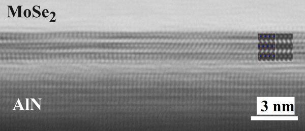
9 Cross section HRTEM-II 6.5Å [1-100] 3L [11-20] [11-20] 7
10 Intensity (a.u.) Intensity (a.u.) XPS-Interfaces and Band Offsets AlN/ 1ML MoSe 2 fitting curve Background ev (3d 3/2 ) ev (3d 5/2 ) Se3d Se-Mo bonds vacuum CB AlN 1L MoSe 2 c = 2.1 ev 3.9 ev Band Offsets Kraut s method CBO = 1.81 ev CB Binding Energy (ev) E F 6.2 ev 1.58 ev VB AlN/ 1ML MoSe 2 fitting curve Background Mo-Se bonds ev (3d 5/2 ) Mo3d VB VBO = 2.84 ev (3d 3/2 ) Binding Energy (ev) The peaks show Mo-Se bonds only. There is no clear sign for a reaction between MoSe 2 and the AlN substrate Sufficiently large BO- no charge transfer 8

 k x,// (Å -1 )")
11 Binding energy (ev) Binding Energy (ev) Binding energy (ev) k z Valence Band Imaging- in situ ARPES 1 ML E F Direct G K G G K G/A K/H 1ML 6 ML He I ~21 ev He I ~21 ev K 1ML k x,// (Å -1 6 ML ) k x,// (Å -1 ) L M A Γ K H k //, x MoSe 2 1 st Brillouin zone He II ~40 ev He II ~40 ev k x,// (Å -1 ) k x,// (Å -1 ) 9
12 Intensity (a.u) Intensity (a.u) Raman and RT Photoluminescence High quality single or bi- layer MoSe 2 Evidence for direct gap Excellent stability in air (>2 weeks uncapped) MoSe 2 A 1g cm -1 Raman Si 521 cm K =532 nm 2 mw Point 1 Point 2 Point K =532 nm 2 mw Photoluminescence A (1.55 ev) Point 1 Point 2 Point 3 B (1.75 ev) 190 mev Raman Shift (cm -1 ) A B Energy (ev) G Κ M 10
13 Raman peak intensity (a.u.) PL peak intensity (a.u.) log(intensity) (a.u.) Intensity (a.u.) Large Scale Uniformity Digital behavior : either High or Low High Low A 1g E 1 2g Si B 1 2g 0.3cm 0.5cm 0.7cm 0.9cm 1.1cm 1.3cm Breathing mode High Low Distance from sample edge 0.3cm 0.5cm 0.7cm 0.9cm 1.1cm 1.3cm Raman shift (cm -1 ) Wavelength (nm) High Raman Low PL (bi layer?) MoSe2 peak intensity Intensity largest PL peak Low Raman High PL (single layer?) On the large scale there are two different areas with different thickness? Distance from edge 11
 R ~ 20-30 Ohm-cm a bit high,")
14 Sheet resistance R sh (MOhm/sq) resistivity (Ohm cm) MoSe 2 Resistivity TLM, 4-probe, vd Pauw Au contacts, e-beam + lift-off MoSe 2 /200 nm AlN/Si RT = R sh d MoSe 2 Thickness (ML) R ~ Ohm-cm a bit high, intrinsic 12
15 PART B Epitaxial MoSe 2 /HfSe 2 Heterostructures on AlN Growth of HfSe 2 directly on AlN Growth of heterostructures 13
 MoSe 2 /HfSe 2 MoSe 2 /ZrSe 2 Type II broken gap")
16 Motivation C. Gong et al., Appl. Phys. Lett. 103, (2013) MoSe 2 /HfSe 2 MoSe 2 /ZrSe 2 Type II broken gap band alignment TFET 14


17 Epitaxial Growth of HfSe 2 4L HfSe 2 4L HfSe 2 AlN 2L MoSe 2 AlN AlN AlN 4L HfSe 2 2L MoSe 2 T growth = 570 C T g = 350C + T ann =690 C 4L HfSe 2 4L HfSe 2 T UHV anneal = 810 C T g = 350C + T ann =690 C 15
 1")
 4 L HfSe 2 E g ~0.")
18 E B (ev) Electronic band structure 4L HfSe 2 AlN Similar quality for HfSe 2 /MoSe 2 /AlN E (ev) 1 L HfSe 2 Μ Κ Γ Μ Γ E g ~0.53 ev E g > 0.9 ev? E (ev) 4 L HfSe 2 E g ~0.41 ev k //,x (Å -1 ) Κ Γ Μ 16
19 PART C Epitaxial Bi 2 Se 3 Topological Insulators and Bi 2 Se 3 /MoSe 2 multilayers High quality epitaxial growth on AlN Observation of Dirac cone in ultrathin Bi 2 Se 3 High quality Bi 2 Se 3 /MoSe 2 multilayers 17

 Thin ~ 3")

20 Cross section HRTEM P. Tsipas et al., ACS Nano 8, 6614 (2014) Thick ~ 20 Quintuple Layers (QL) Thin ~ 3 QL 1 QL ~ 0.96 nm [11-20] Se Bi 1 QL High epitaxial quality and clean crystalline interfaces 18
 Γ E F CB Μ 2 nd")

 Spin-polarized Possible new")
21 E B (ev) Surface Dirac cone Μ 3 QL Bi 2 Se 3 /AlN(0001) Γ E F CB Μ 2 nd derivative Gapless metallic surface states insulating bulk 0.47 ev spin VB k //,y (Å -1 ) k //,y (Å -1 ) Spin-polarized Possible new spin functionalities 19


![AlN [11-20]](/docs-images/88/115048099/images/22-5.jpg "azimuth 6.")
22 MoSe 2 /Bi 2 Se 3 Multilayers RHEED MoSe 2 at 300 o C Bi 2 Se 3 at 300 o C AlN [11-20] azimuth 6.5 Å 5 QL 20
23 Summary/conclusions 2D selenide materials heterostructures by MBE on crystalline dielectric AlN substrates MoSe 2 semiconductors HfSe 2, ZrSe 2 semiconductors Bi 2 Se 3 topological insulators Atomically thin Single crystalline and uniform over large areas Stable in air (MoSe 2 ) 21