Amorphous Si/Au wafer bonding P. H. Chen 1, C. L. Lin 1 and C. Y. Liu 1,2. National Central University, Jhong-Li, Taiwan, R. O. C.
|
|
|
- Hubert Merritt
- 5 years ago
- Views:
Transcription
1 Amorphous Si/Au wafer bonding P. H. Chen 1, C. L. Lin 1 and C. Y. Liu 1,2 1 Dept. of Chemical Engineering and Materials Engineering, 2 Institute of Materials Science and Engineering, Abstract: National Central University, Jhong-Li, Taiwan, R. O. C. Crystal (100)-Si/Au and amorphous Si /Au bonding for wafer bonding applications were studied. It was found that large craters and air voids could form at the c-si/au bonding interface. However when the (100) Si wafer was coated with an amorphous Si layer the craters that formed at the bonding interface were smaller and more uniformly distributed. Remarkably, no voids could be observed at the amorphous Si/Au bonding interface. We believe that the uniformity of the Au(Si) liquid alloy was a result of the fast amorphous Si/Au reaction and that this is the key to achieving a void-free bonding interface. In other words a uniform liquid Au(Si) eutectic that slowly reacts with the (100) Si prevents air void formation at the bonding interface.
2 Introduction: Au-Si eutectic bonding has been successfully used in IC (Integrated Circuits) packaging and MEMS applications, such as for sealing, die attachment and electrical interconnects. [1] Recently, Au-Si eutectic bonding has also been implemented into wafer bonding techniques. [2, 3] The requirements for wafer bonding are much stricter than those for conventional die attachment and sealing applications. A uniform and void-free bonding interface is required for successful wafer bonding. Jang observed however, that voids and craters often formed at the Au-Si bonding interface. The presence of voids at the bonding interface has a serious affect on the reliability of the bonding layer and the performance of the bonded wafer device. [4, 5] So, to make Au-Si bonding practical for wafer bonding applications, the problem of voiding at the Au/Si bonding interface has to be solved. [6] The length of the Au-Si wafer bonding process is another issue that must be dealt with. The formation of the Au-Si bond is highly dependent on the inter-diffusion rate between Au and Si. It usually takes over 15 minutes to accomplish the bonding process. The Au-Si bonding process is typically done at a temperature of 400, 40 over its eutectic point (363 ). [3] This means that delicate devices on the wafers are likely to suffer thermal damage during the wafer bonding process. In this paper, we report a novel Au/amorphous Si bonding process with which it is possible to achieve void-free Au-Si eutectic wafer bonding. Experiments: Figs. 1(a) and (b) show schematics of the two bonding structures studied in this work. A 1-μm amorphous Si layer was deposited on a (100)-Si wafer by the PECVD (Plasma Enhanced Chemical Vapor Deposition) process. To ensure good adhesion between the Au layer and the Si wafer, a Cr/Pt bi-layer was deposited on
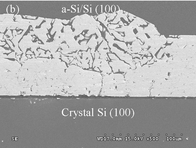
3 the Si wafer prior to the E-Gun deposition of the Au seed layer and subsequent to Au electroplating. A 10-μm Au layer was electroplated on the E-Gun Au seed layer. Then using graphite bonding fixtures, the Au/Pt/Cr/Si wafers were respectively bonded with cleaned crystal (100)-Si (c-si) wafers and amorphous Si coated Si wafers (a-si). A graphite bonding fixture was used to apply the proper bonding force to the two bonded Si wafers. The entire bonding process was performed in a vacuum furnace maintained at around torr throughout. After the specified bonding times, the bonded Au-Si samples were removed from the bonding fixture and mounted with epoxy for SEM cross-sectional examination. Results and Discussion: Fig. 2 shows cross-sectional SEM images of the a-si/au and c-si/au bonded samples. As shown in Fig. 2(a), we can observe relatively big craters at the bonding interface of the c-si/au sample. Facet crater formation at the c-si(111)/au bonding interface has been observed by Jang. [6] Owing to the anisotropic nature of crystalline Si, the c-si/au reaction rate is highly dependent on the crystallography of the Si wafer. In other words, Si dissolution into the Au layer proceeds preferentially along particular planes, usually the planes with the highest surface energy. [6] In crystalline Si, the (111) plane has the lowest surface energy, so is the most resistant to dissolving in Au. This means that, as Si reacts with and dissolves in Au, facet craters, i.e., V-shape grooves or inverted pyramids form on the c-si surface. Fig. 2(a) shows inverted-pyramid craters that formed on the (100) Si side; they are constructed of four (111) Si planes. In addition, observe that big air voids formed inside the craters. Note that the densities of Si and Au(Si) liquid alloy are very different, 2.33 g/cm 3 and g/cm 3, respectively.[7] We believe that the formation of air voids in the craters is associated with the fact that there is density mismatch between the c-si and the
4 Au(Si) alloy. As Si dissolves into Au during the Au-Si bonding process, the incremental volume of the Au(Si) alloy is insufficient to compensate for the volume of Si consumed, which means that the amount of liquid Au-Si alloy formed does not completely fill the craters in the Si side. Thus, air voids will form inside the craters at the bonding interface, as seen in Fig. 2(a). Those air voids result in a weak bonding interface and poor thermal and electrical conductivity across the bonding interface. As seen in Fig. 2(b), there are much smaller craters at the bonding interface than for the c-si/au case and, remarkably, no air voids can be found in the craters. We suggest that the primary reason for the void-free quality of the bonding interface is the fast formation of a uniform layer of Au-Si liquid alloy. Due to the looseness of the structure of the amorphous Si coating layer, the dissolution of Si into Au can occur at a very fast rate, without any preferential orientation. After the rapid consumption of the a-si coating layer to form a liquid eutectic Au-Si alloy, the Au(Si) liquid alloy would start to react with the underlying c-si wafer. Since the liquid Au-Si alloy already contains a certain amount of Si, the reaction rate of the c-si/au-si liquid alloy would be much less than that of the c-si/au reaction case. The slow c-si/au-si alloy reaction prevented the formation of large craters on the c-si side, also making it unlikely for air voids to form at the bonding interface. Prior to examining the reactive Si surfaces, we used an aqua-regia solution to remove the Au(Si) bonding layer. Fig. 3(a) shows the exposed Si surface for the c-si/au bonding case. Relatively big craters can be seen on the c-si bonding surface. The distribution of the crater size is quite large; it ranges from 10 μm to 90 μm. On the other hand, the craters on the a-si surface are much smaller and uniformly distributed. Fig. 4 shows SEM cross-sectional images of the edged of the bonded samples. As seen in Fig. 4(a), the eutectic Au-Si alloy exhibits excellent wetting on
5 the a-si surface. The wetting angle is about 17 o. In contrast, the c-si surface of the eutectic Au-Si alloy does not seem to wet well. Above we have shown that a fast a-si/au reaction is the key to the prevention the formation of air voids in craters at the Si/Au bonding interface. The rates of a-si/au and c-si/au reactions in a prepared c-si/au/a-si sandwich structure were compared. The sandwich sample was then annealed at 380 for 2 minutes. Remarkably, the thin amorphous Si coating reacted substantially with Au, as shown in Fig. 5, while, no reaction was observed on the opposite c-si side. The implication is that fast Au/a-Si inter-diffusion greatly reduces the incubation time necessary for the formation of eutectic Au-Si bonding. There are two reasons for faster formation of a Au(Si) liquid alloy at the a-si/au interface. First, Au atoms have a much faster diffusion rate in Au. Second, it takes much less energy to release Si atoms in amorphous Si than in crystalline Si. Conclusions: An amorphous Si coating layer on a (100) Si wafer rapidly reacted with the Au layer to form a uniform Au(Si) liquid alloy, which prevented the formation of voids at the bonding interface. This amorphous Si/Au bonding process should enable the implementation of Si/Au bonding in wafer bonding applications. References: [1] A.L. Tiensuu, M. Bexell, et al., Sensors and Actuators A, 1994; 45: 227. [2] R.F. Wolffenbuttel, K.D. Wise, Sensors and Actuators A, 1994; 43: 223. [3] R.F. Wolffenbuttel, Sensors and Actuators A, 1997; 62: 680. [4] D.S Gardner, P.A. Flinn, Electron Devices, 1988; 35: 2160 [5] K.Hinnode, I. Asano, Y. Homma, Electron Devices, 1989; 36: 1050.
6 [6] Jin-Wook Jang, Scott Hayes, Jong-Kai Lin, and Darrel R. Frear, Appl. Phys., 2004; 95: [7] William D.Callister, Jr., Materials Science and Engineering an Introduction (Wily), appendix A.


7 Fig. 1 Fig. 2


8 Fig. 3


9 Fig. 4

10 Fig. 5
11 Captions: Fig. 1 The structure of bonding test. (a) is the c-si(100) bonded with Au lauer and (b) is pre-deposit 1μm a-si on c-si(100). The Cr and Pt can ensure adhesion and be a barrier layer Fig. 2 Cross section image of (a) crystal Si-Au bonding (b) amorphous Si-Au bonding. The voids that relative big void can be fined in crystal case. Fig. 3 The bonding interface of (a) crystal Si-Au bonding (b) amorphous Si-Au bonding. The amorphous Si-Au bonding has more uniform size and distribution of craters. Fig. 4 Cross-section image of both bonding case. Case (a) is the c-si/au bonding. Au-Si allow seem not wetting on c-si surface. Case (b) is the a-si/au bonding. Au-Si alloy spread out on the a-si surface. Fig. 5 The SEM image of rate determine test. The degree of reaction that in amorphous Si side is higher than crystal side.