Epitaxial 2D SnSe 2 / 2D WSe 2 van der Waals Heterostructures
|
|
|
- Alexander Brown
- 5 years ago
- Views:
Transcription
1 SUPPORTING INFORMATION Epitaxial 2D SnSe 2 / 2D WSe 2 van der Waals Heterostructures Kleopatra Emmanouil Aretouli,, Dimitra Tsoutsou, Polychronis Tsipas, Jose Marquez- Velasco,, Sigiava Aminalragia Giamini,, Nicolaos Kelaidis, Vassilis Psycharis, and Athanasios Dimoulas *, Institute of Nanoscience and Nanotechnology, National Center for Scientific Research DEMOKRITOS, 15310, Athens, Greece University of Athens, Department of Physics, Section of Solid State Physics, Athens, Greece National Technical University of Athens, Department of Physics, Athens, Greece AUTHOR INFORMATION Corresponding Author *a.dimoulas@inn.demokritos.gr S -1


2 (a) (b) Figure S1 Schematic representation of the structure of 1T-SnSe 2 crystal: (a) side view (b) top view. The unit cell contains only one layer. S -2
3 Figure S2 For thickness calibration purposes, X-Ray Reflectivity measurements were performed on a Rigaku Smart Lab diffractometer at thick (nominal 8ML) control samples SnSe 2 (A1) and WSe 2 (A2), grown directly on AlN/Si(111) substrates in order to avoid interference with reflection oscillations from the Bi 2 Se 3 template. The analysis of measurements was performed using the Global Fit program 1. At the early stage of analysis the Global optimization method was used and the final models were obtained using the nonlinear least squares fitting method 1. In the analysis of the reflectivity curves for each sample a layer deposited on an AlN substrate it was considered. The best results were derived by considering a linear variation of the density of the top layer from the surface down to the interface with AlN layer. Figure S3 Spectroscopic ellipsometry (SE) (FLS-300) J. A. WOOLAN) measurements for the thickness determination of thin samples A3 and A4, which are 4ML WSe 2 and SnSe 2 respectively, and for the thick A2 sample in order to compare XRR with SE technique.the analysis of the data was done using the CAUCHY model. In Figs.S3(a-c) the experimental amplitude ratio Ψ and phase difference Δ versus wavelength (solid lines) and the fitting curves(dashed lines) are plotted and the results are summarized in Table S1. S -3
4 structure Nominal Thickness Thickness thickness (nm) XRR (nm) Ellipsometry (nm) A1 8ML SnSe A2 8ML WSe A3 4ML WSe A4 4ML SnSe Table S1 XRR and SE results for thickness determination. In the case of SnSe 2, a thickness of 2.67 nm is deduced which is in good agreement with the nominal thickness of 2.45 nm (4ML). In the case of WSe 2 there is a small deviation: a thickness of 3.0 nm is deduced instead of the nominal value of 2.6 nm expected based on XRR calibration from thicker samples. This discrepancy may be explained based on the fact that SE overestimates thickness with respect to XRR as has been previously reported 2. To verify this in our samples, we measured the thicker sample A2 of 8ML WSe 2 by both XRR and SE and we found that the latter technique yields a thickness by 0.53 nm larger than that obtained by XRR (see table S1). This indicates that the discrepancy in the measured thickness for the nominal 4ML WSe 2 sample is within the uncertainty which is inherent in the measurement of small thickness by XRR and SE techniques. Therefore we estimate that both thicknesses measured by SE are close to the nominal value. It's worth noting that, the refractive indices (a n ) of SnSe 2 and WSe 2 are estimated to be 2.99 and 3.7, respectively at 632 nm, which are close to reported values for these materials 3, 4. S -4
5 Figure S4 Raman spectrum of SnSe 2 /WSe 2 /Bi 2 Se 3 heterostructure. The Bi 2 Se 3 buffer layer gives a very strong Raman spectrum overlapping with the Raman peaks of SnSe 2 and WSe 2, eventually masking them. Figure S5 XRD scans recorded for the thick (8 ML) WSe 2 and SnSe 2 layers grown directly on AlN substrates which were grown for the purpose of thickness estimation by XRR. XRD and XRR on WSe 2 and SnSe 2 layers grown on Bi 2 Se 3 template suffer from complications due to the presence of Bi 2 Se 3 related peaks and interference oscillations. Therefore we can only present the XRD patterns recorded for the 8 ML WSe 2 /AlN and 8 ML SnSe 2 /AlN structures, as shown S -5

6 below. In both cases, sharp diffraction peaks originating from the AlN/Si(111) substrate are observed, as expected. Despite the inferior quality of WSe 2 and SnSe 2 films on AlN as compared to those grown on Bi 2 Se 3 (see related discussion in RHEED of Fig. 2), well resolved peaks, especially for WSe 2 are observed such as (001),(002) and higher order diffraction indicating that [001] WSe 2 (SnSe 2 )//[0001]AlN along the growth direction. Figure S6 RHEED patterns along [10-10] azimuth of the 4ML WSe 2 (SnSe 2 )/ 5QL Bi 2 Se 3 /AlN Si(111) samples. The patterns are streaky at both azimuths so there is no evidence of 3D island formation. Nevertheless, the RHEED patterns of SnSe 2 although they are streaky in general, their intensity is not fully uniform along the streaks which may indicate 2D island formation in compatibility with the morphology imaged by STM. S -6
 (d)")
7 (a) (b) (c) (d) (e) S -7
 1500x1500μm 2, (c) 270x270μm 2, (d) 130x130μm 2 and (e) 55x55μm 2 as were recorded from the middle of the sample.")
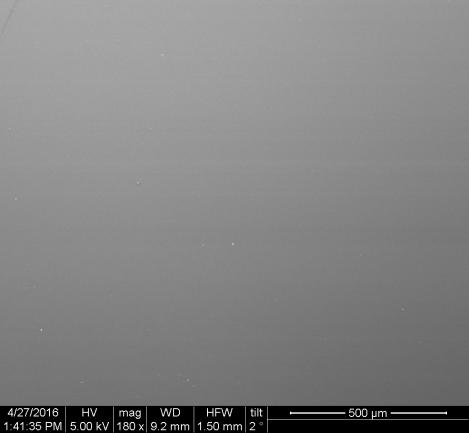
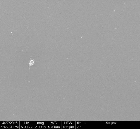
8 Figure S7 SEM images showing the surface of SnSe 2 /WSe 2 /Bi 2 Se 3 heterostructures, with areas (a) 330x330μm 2, as recorded from the corner of the sample showing and AlN substrate. This area is masked by the sample holder and remains uncovered. (b) 1500x1500μm 2, (c) 270x270μm 2, (d) 130x130μm 2 and (e) 55x55μm 2 as were recorded from the middle of the sample. It can be seenthat the films are continuous over large areas on the substrate. S -8
9 Figure S8 DFT band structure calculations of (a) 4 ML 2H-SnSe 2 with D 6h (P63/mmc) symmetry and (b) 1ML orthorhombic SnSe (Pnma) phase free-standing slab with spin orbit coupling. DFT predicts that 2H-SnSe 2 is metallic in contrast to the case of 1T-SnSe 2 bandstructure where a semiconducting band gap of 0.4eV (GGA) was obtained (Fig. 3(c)). The orthorhombic SnSe band structure indicates a semiconductor material. Both phases in S8 (a) and (b) below are distinctly different from our experimentally derived SnSe 2 band structure, presented in Fig. 4(a) in the main text. The corresponding Brillouin zone for SnSe 2 hexagonal(c) and SnSe orthorhombic (d) crystal lattices. S -9
 sample, the complete mapping of which is presented in Fig. 4(a).")
 and corresponds to the small peak near the Fermi level observed in the linescan (k x =0.9 Å -1 ) shown in Fig. 4(d).")

10 Figure S9 Enhanced contrast ARPES image of the valence band structure along the ΓΜdirection of the Brillouin zone for the 4 ML SnSe 2 /Bi 2 Se 3 /AlN/Si(111) sample, the complete mapping of which is presented in Fig. 4(a).The onset of the conduction band minimum is visible at the M point (k x,// =0.9 Å -1 ) and corresponds to the small peak near the Fermi level observed in the linescan (k x =0.9 Å -1 ) shown in Fig. 4(d). From S9 below, it can be seen that E F is located at or just above the conduction band minimum indicating that the MBE-grown SnSe 2 is a strongly n- type material. (a) (b) Figure S10a-b Schematic illustration of the proposed device layer structure consisting of the fully epitaxial 2D WSe 2 /2D SnSe 2 /Bi 2 Se 3 /AlN/Si(111) materials combination. As already S -10
11 mentioned in the main text, the Bi 2 Se 3 buffer layer was introduced in order to achieve a good crystalline quality of the epilayers. However, since Bi 2 Se 3 is conductive, it can serve as a bottom electrode in TFET device implementation. The structure in reverse order where WSe 2 is first grown followed by SnSe 2 top layer is also a suitable combination yielding similar band alignments. The final choice should be made taking into account layer stability in air and device processing flow. REFERENCES (1) Rigaku Corporation, X-Ray Reflectivity analysis Program, Global Fit Version , (2) Kohli, S.; Rithner, C. D.;Dorhout, P. K.; Dummer, A. M.; Menoni, C. S.;Comparison of nanometer-thick films by x-ray reflectivity and spectroscopic ellipsometry,rev. Sci. Instrum2005, 76, (3) Garg, A. K.; Agnihotri, O. P. ; Jain A. K.; Tyagi, R.C.; Optical absorption spectrum of tin diselenide single crystals, J. Appl. Phys. 1976, Vol. 47, 997. (4) Eichfeld, S. M.; Eichfeld, C.M.; Lin, Y-C; Hossain, L.; Robinson, J. A.; Rapid, nondestructive evaluation of ultrathin WSe 2 using spectroscopic ellipsometry, APL Mater.2014, 2, S -11