SiC high voltage device development
|
|
|
- Ferdinand Henderson
- 5 years ago
- Views:
Transcription
1 SiC high voltage device development KERI Power Semiconductor Group
2 outline 1. Device design & simulation for power devices 2. SiC power diode process development Ion implantation & activation optimization SiC PiN diode SiC JBS diode Process optimization & results 3. Oxide research for SiC power MOSFETs 4. SiC epitaxy

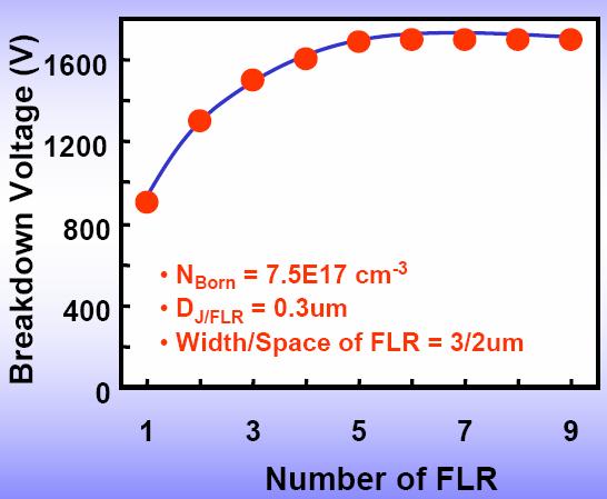
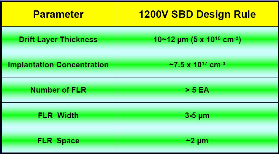
3 1200V device Simulation Guard Ring effect BV dependence on number of FLRs
4 Ion implantation condition sample I/I condition [scheme] Annealing [ o C] JJ6 JBS=Al19, FLR=Al JJ7 JBS=Al19, FLR=Al JA6 JBS=Al19, FLR=Al JA7 JBS=Al19, FLR=Al JB6 JBS=Al19, FLR=B JB7 JBS=Al19, FLR=B JBS : Al ion, surface doping concentration(implanted) cm -3, junction doping concentration cm -3 ( Al19) FLR : Al or B ion, surface doping concentration cm -3, junction doping concentration cm -3 (Al17, B17)

5 Ion implantation mask design Side implantation when the SiO 2 mask is removed by wet etching SiC I/I mask (SiO 2 /Ti/Au) SiO 2 mask Bad aspect ratio Side implantation effect Trench formation Au mask Peeling-up problem Additional SiO 2 layer : suppress reaction between Ti & SiC Protect side implantation Suppress trench formation Suppress Au Peeling-up Stable at high temp.

6 High-temperature activation of Ion Implanted SiC SiC dummy wafer SiC sample Argon atmosphere graphite Al,B: N : (Argon pressure ~600 torr)
7 Current Density [A/cm 2 ] 3.5x o C 3.0x o C 2.5x x x x x10 0 Activation annealing condition dependence Current[A] 4.0x x x x o C 1700 o C Forward Voltage[V] Reverse Voltage[V] Device annealed at 1700 Too long diffusion length decrease of schottky area R on increase Device annealed at 1600 is not fully activated Failure at metal layer not at pn junction

8 0.6um High R on due to diffusion? 2.6um 3.4um FESEM image of devices after 1700oC annealing Width of JBS increased by 0.4 um decreasing schottky area Theoretical analysis of R on with schottky area variation Lateral diffusion of implanted ions reduces the schottky area increase of R on

9 Interface layer formation during annealing interface layer changes the metal/sic contact property from schottky to ohmic harsh environment produce more interface layer the interface layer could be conductive


10 Interface layer formation Good adhesion Extreme case the interface layer deteriorate the metal/sic adhesion
11 Interface layer formation mechanism and its proposed solution High temperature annealing Removal of interface layer by dry etching C-rich layer was formed due to preferred sublimation of Si-species during high temperature annealing Non-stoichiometric interface layer provide leakage current path Using ICP-RIE with low damage condition, stable SiC devices were produced without interface layer
 1. SF 6 /O 2 or CF 4 /O 2 2.")
 Selectivity > 10:1 (metal mask: SiC) Etch rate")
12 Surface treatment for removing an interface layer ICP-RIE system for SiC etching (Oxford ICP65 system) 1. SF 6 /O 2 or CF 4 /O W RF power generator, 600W ICP power generator Etch condition for removing interface layer Metal mask (Ni, Al) Selectivity > 10:1 (metal mask: SiC) Etch rate ~100nm/min Surface roughness: 1.6nm (RMS)
13 Interface layer analysis: reverse characteristics Surface treatment using ICP removed the interface layer formed during high temperature, leading to lower leakage current and higher breakdown voltage
14 Current[A] 4.0x x x x Breakdown voltage of JBS diode space 3um space 9um BV decrease with schottky area increase higher trap density lower schottky barrier -1.0x Reverse Voltage[V] BV with variation of space between JBS lines
15 Measurement set-up for measuring the pico-ampere-level leakage current Reverse Leakage Current [A] x x x x x Reverse Bias Voltage [V] Reverse Leakage Current [A] Si FRD SiC Cree(600V) SiC Cree(1200V) Reverse Bias Voltage [V] Si FRD SiC Cree(600V) SiC Cree(1200V) Measured Reverse leakage characteristics of commercially available SiC SBDs and Si FRD


 Si FRD (b) SiC")

 channel 3 (purple):")
16 Measurement set-up for measuring the pico-ampere-level leakage current Measured reverse recovery characteristics of commercially available SiC SBD and Si Diodes < 20ns <15ns (a) Si FRD (b) SiC SBD (600V) > 640ns (c) Si Diode time scale: 40ns/div for (a) and (b), 80ns/div for (c) channel 3 (purple): current flowing through DUT in 1A/V

17 Thermal analysis of packaged device power devices
18 Distribution of Interface-Trap Density power devices
19 Comparison of critical Electric field Nitrided thermal oxide showed ideal critical electric field
20 Dependence of device proces parameter (RTA process, D it ) The interface properties of thermally grown nitrided oxide was not deteriorated ded after device process

21 Initial growth (on-axis substrate) 1600 o C, 3min deposition Optical microscopy reflective 50μm Crossed-polar transmission circular-shaped etch pits were formed in the vicinity of micropipes. Some of them shows spiral structure which is thermodynamic equilibrium shape, especially in the growth mode.


22 H 2 etching (on-axis substrate) 1600 o C, 3min Optical microscopy reflective 20μm Crossed-polar transmission The region near micropipes was etched with non-circular shape. There is another driving force for etching the SiC surface.


23 Typical etch pit morphology No step bunching Well developed step bunching Bright region is low doped grown SiC epitaxial film and the dark region is high n-doped substrate. It is clear that the region near micropipes was etched not deposited. Two types of etched micropipe were found. the reason was not cleared, yet.


 with")
24 Shapes of micropipe etch pits 30μm Etch pit revealed by KOH etching 220nm 160nm Etch pit revealed at initial growth stage The etch pits formed during initial growing stage showed bellybutton-shape, however the pits formed by KOH etching shows hexagon. The size of the micropipe is small(~200nm in diameter) with respect to usual one (~ several mm in diameter).
 (b) Spirals (a) etched surface and (b)")

25 Spiral shape in the vicinity of micropipes (a) (b) Spirals (a) etched surface and (b) grown surface. The spiral on the grown surface shows more clear steps, i. e., higher step heights
26 Nearly on-axis substrates Nearly on-axis substrates provide wide enough terraces for spiral formation. Circular-shaped sprial etch pits formed in the vicinity of micropipe
27 Off-axis substrates The surface steps, which is formed parallel each other, break the continuous step of spiral. Consequently, the spiral is hard to exist on the off-axis substrates
 1600 o C, 30min SiH 4 : C 3 H 8 = 12:3 3.")
 - high speed growth rate achieved (G max = 1um/min) - utilized up")
28 Growth rate & thickness uniformity Epi-layer substrate 1660 o C, 11min SiH 4 : C 3 H 8 = 15:5 1.6um (9um/hr) 1600 o C, 30min SiH 4 : C 3 H 8 = 12:3 3.2um (6.5um/hr) - high speed growth rate achieved (G max = 1um/min) - utilized up to 1inch substrate - adaptation of 2 inch substrate is remained project
29 Summary 1. design optimization 2. 2kV PiN, 1.2kV JBS diode was achived 1. Further research : development of devices for higher current capability 3. Obtaining high quality thermal oxide was achieved which can be utilized to SiC power MOSFETs 1. Further research : development of high speed switching devices 4. Home made SiC epitaxy layer will be used for power devices