Fabrication of high power GaN transistors F. Medjdoub CNRS - IEMN
|
|
|
- Kathryn Manning
- 5 years ago
- Views:
Transcription


1 Fabrication of high power GaN transistors F. Medjdoub CNRS - IEMN E. Dogmus, A. Linge, T. Defais, R. Kabouche, R. Pecheux, M. Zegaoui


2 Lille city centre Where are we?


3 National Network of Large Technological Facilities for Basic Technological Research
4 o Introduction o Device design for high power devices o Description of the device fabrication o Main processing techniques o Main technological bricks o How to further push the breakdown limits of GaN-on-Si HEMTs o LSR approach developed within Inrel project o Conclusion


5 Gallium nitride is probably the most important new semiconductor since silicon save energy, carbon emissions and enable totally secure communications blue, green, yellow, red LEDs by adding more and more Indium to GaN GaN superior to other semiconductor for both power and RF applications owing to its outstanding intrinsic properties

6 Breakthrough in terms of power performances Much higher current density and voltage operation

7 Inherent surface charges causing 2DEG depletion and degradation of performances and/or device reliability
8 Device technology In - situ SiN cap layer Thick in-situ SiN cap layer barrier layer GaN channel BUFFER Transition layers High electron confinement under high electric field Substrate o Buffer layers specifically designed to enhance the electron confinement while avoiding deep traps o Thick SiN cap layer used to improve the device robustness, especially to avoid gate leakage current increase after full passivation


 800 1000")


9 N S_Change (%) Benefit of in-situ SiN cap layer 10 0 Si 3 N 4 cap AlGaN GaN Before After SiN cap GaN cap Uncapped temperature ( C) EXPERIMENT : The temperature was ramped up in vacuum to 900 C using a step of 100 C for 30 min. After each step Hall measurement was performed at RT. GaN Cap Layer AlGaN GaN Si 3 N 4 Cap Layer AlGaN GaN

10 Benefit of in-situ SiN cap layer Thick in-situ SiN = key parameter for low dispersion and high stability 0.5 µm AlGaN/GaN-on-silicon technology V T 500 ns pulsed 325 C G 325 C Low dispersion and High thermal stability above 300 C (attributed to the in-situ SiN cap layer)
11 Current (A) 60 µm circular diodes w and w/o 100 nm PECVD SiN passivation PECVD SiN (100 nm) SiN cap layer (2 nm) Ultrathin barrier layer spacer layer GaN channel Buffer layers seed layer Substrate 2 nm cap SiN passivated 2 nm cap SiN unpassivated nm cap SiN passivated 17 nm cap SiN unpassivated PECVD SiN (100 nm) SiN cap layer (17 nm) Ultrathin barrier layer spacer layer GaN channel Buffer layers seed layer Substrate Voltage (V) o o after SiN PECVD passivation: Strong and systematic degradation of gate leakage and early breakdown when using thin SiN cap layer of couple of nm. Almost no degradation of gate leakage when using thicker SiN cap layer.
12 Proposed leakage current mechanism after full passivation G Ex situ SiN Passivation Interface charges Electron injection at the MOCVD SiN / PECVD SiN interface under high electric field creating a conducting path at this location S In-situ SiN D Barrier layer GaN Channel Buffer layers Substrate 2DEG A critical in-situ SiN cap layer thickness is needed to prevent the electron injection under high electric field
13 o Introduction o Device design for high power devices o Description of the device fabrication o Main processing techniques o Main technological bricks o How to further push the breakdown limits of GaN-on-Si HEMTs o LSR approach developed within Inrel project o Conclusion
14 Design and fabrication of power devices Mask set for fabrication Fabrication chip reverse engineering Design Manufacturer Finish packaging Test IC Start Mask layout Specifications


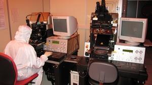
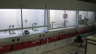
15 Cleanroom: fully controlled environment o Controlled level of contamination, humidity, temperature, pressure, chemicals etc. o to 1 million times less particles than outside o Personnel working in cleanrooms undergo extensive training in contamination. They enter and exit the cleanroom through airlocks, air showers. They must wear special clothing designed to trap contaminants that are naturally generated by skin and the body (boots, shoes, coveralls, face masks, gloves, hoods, and shoe covers)

16 Cleanroom: fully controlled environment Cleanrooms are classified by how clean the air is EU standards Foundry ONSEMI IEMN No human presence! Automation of all technological steps Manual operators Allows to achieve demonstrators / prototypes in small quantity
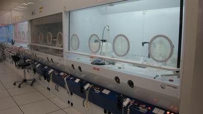
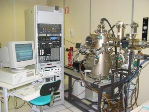
17 Cleanroom tour: Triquint (GaN RF manufacturer)
 Wet and dry etching Ion implantation Wafer back-grinding (thinning) Chemical-mechanical")
18 Device fabrication techniques Today, GaN-on-Si power devices are fabricated on wafers up to 8-inch, which allows generating hundreds of devices simultaneously Basic processing steps: o o o o o o o o o o o o Wet cleans Photolithography Metal deposition Thermal treatments Physical vapor deposition (PVD) Wet and dry etching Ion implantation Wafer back-grinding (thinning) Chemical-mechanical planarization Electroplating Wafer dicing and mounting Die bonding 200 mm


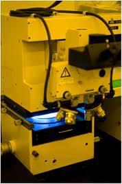
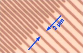
19 Photolithography (optical) o Enables to pattern parts of a thin film or the bulk of a substrate o Uses light to transfer a geometric pattern from a photomask to a lightsensitive chemical "photoresist with a resolution of 0.5 to 1 µm o Chemical treatments reveals the exposure pattern, or enables deposition of a new material in the desired pattern

20 Photolithography (optical)


21 Photolithography (stepper) step-and-repeat camera used in the manufacture of integrated circuits Use alignment marks to align each reticles with a resolution down to hundreds of nm


22 Electron-beam lithography Scanning a focused beam of electrons to draw custom shapes on a surface covered with an electron-sensitive film No mask required! The primary advantage of electron-beam lithography is that it can draw custom patterns (direct-write) with sub-10 nm resolution High resolution BUT low throughput limiting its usage to photomask fabrication, low-volume production of semiconductor devices, and research and development
. No efficient wet etching solutions for GaN Dry etching: lower cost, anisotropic (1 direction).")
23 Etching Important factors: Uniformity Etch rate and control Etch selectivity Advantages and Disadvantages of Dry (plasma) and Wet etching Wet etching provides low damage, high selectivity, simple equipment BUT generally isotropic (etching in all directions). No efficient wet etching solutions for GaN Dry etching: lower cost, anisotropic (1 direction). However, plasma damages and re-deposition of no volatile compounds have to be overcome when used in the active parts of devices


24 Etching Isotropic silicon wet etching GaN Dry Etching Process

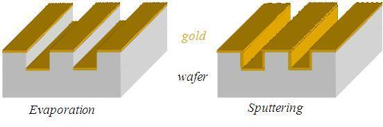
25 Metal deposition Two techniques to obtain the patterns by metallization : Etching Lift-off 1. Metallization of the substrate 2. Photolithography to define the patterns with a mask 3. Etching the metal in the open areas 4. Remove the resist with solvent 1. Bilayer resist 2. Photolithography to define the patterns with a mask 3. Exposure in order to open the areas and creation of an undercut due to difference in resist sensivity. 4. Metal deposition that will lift-off on top of the resists following removal with solvent

26 Metal deposition Evaporation: Metal is melted in vacuum and evaporated to the sample through vacuum. Very common in III-V semiconductors, ideal for lift-off Deposition rate depends on pressure, temperature and atomic mass of species. Sputter deposition: Physical vapor deposition consisting in ejecting material from a "target" onto a "substrate. The sputtering gas is often an inert gas such as argon. Better step coverage than evaporation
27 Metal deposition Evaporation tool 60 nm Sputtering tool


28 Metal deposition Electro-plating: Used for thick metal deposition several µm to several tenths of µm Uses electric current to reduce dissolved metal cations so that they form a thin coherent metal coating on a conductive surface. Therefore, a seed layer (metal) is used on the area where plating is desired. Cu interconnects through via holes


29 Ion implantation Ions of a material are accelerated in an electrical field and impacted into a solid. Process used to change the physical, chemical, or electrical properties of the solid. The energy of the ions (up to several hundreds kev), as well as the ion species and the composition of the target determine the depth of penetration of the ions in the solid Used for instance: Preparing SOI substrate (high dose oxygen implant is converted to silicon oxide Doping of semiconductors Device isolation

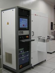
30 Rapid Thermal Annealing Semiconductor manufacturing process which heats wafers to high temperatures (up to 1000 C) on a timescale of several seconds or less Used for formation of ohmic contacts Temperature range : 140 à 1200 C High vacuum


31 PE and LP CVD deposition Plasma Enhanced Low pressure Chemical vapor deposition SiN and SiO 2 deposition highly in GaN device fabrication for passivation or as sacrificial layers
32 o Introduction o Device design for high power devices o Description of the device fabrication o Main processing techniques o Main technological bricks o How to further push the breakdown limits of GaN-on-Si HEMTs o LSR approach developed within Inrel project o Conclusion
33 Basic process flow to fabricate the GaN devices Starting wafer sample Isolation Ohmic metal deposition and RTA Gate deposition Passivation Backside pattern and etch

34 GaN device cross section In-situ SiN cap layer Barrier layer
 and, hence, the power losses of the system Achieving good ohmic contacts in these materials is inherently difficult, due to the wide band gap (3.")
35 Ohmic contacts Ohmic contacts are a fundamental building block of GaN power devices The ohmic contact resistances must be as low as possible in order to minimize the device specific on-resistance (Ron) and, hence, the power losses of the system Achieving good ohmic contacts in these materials is inherently difficult, due to the wide band gap (3.4 ev for GaN) which typically leads to Schottky barrier height values in the order of 1 ev on n-type and even of 2 ev on p-type material. Even more critical in AlxGa1-xN alloys with increased Al content


36 Ohmic contact formation Lithography Schematic band diagram to describe the mechanism of current transport in ohmic contacts to AlGaN/GaN heterostructures Surface treatment or etching Metal deposition (typically Ti/Al based for GaN heterostructures) Rapid flash annealing The model assumes the presence of the modified surface subsequent to the HT annealing. The electrons can easily tunnel through this very thin barrier. The second barrier is the one that the electrons injected in the AlGaN layer have to overcome in order to reach the 2DEG at the AlGaN/GaN interface.


37 How to measure the ohmic contact resistances? Transfer Length Measurement extraction X

38 Au-free ohmic contacts Most common solutions for ohmic contacts, both to GaN and AlGaN/GaN heterostructures, is based on annealed Ti/Al/X/Au multilayers providing R C as low as 0.2 Ω.mm Au cap layer enables to prevent surface oxidation and to improve the contact resistance by the formation of conductive phases inside the entire metal stack However, GaN power devices must be low cost and fully compatible with Si CMOS technology. Therefore, to avoid cross-contaminations in Si devices industry and reduce the overall manufacture cost of the HEMT devices, Au cannot be used recessed Ti/Al/W Ohmic contacts to AlGaN/GaN heterostructures H.-S. Lee, et al, IEEE Electron Device Lett. 32 (2011) 623


39 Device isolation 2 approaches commonly used to isolate GaN devices Mesa: Dry etching in order to define device active regions Mesa sidewalls can lead to increased gate leakage current and reduced breakdown voltage Implantation: Ion implantation in order to define device active regions Planar surface, highly reproducible and stable


40 Gate module: various architectures Normally-off desired for GaN power devices Schottky contact High leakage current Reduced breakdown voltage Normally-on devices Low leakage current Single chip normallyoff transistor Low threshold voltage Low leakage current Single chip normallyoff transistor Device/dielectric not qualified
41 o Introduction o Device design for high power devices o Description of the device fabrication o Main processing techniques o Main technological bricks o How to further push the breakdown limits of GaN-on-Si HEMTs o LSR approach developed within Inrel project o Conclusion

42 How to further push the limits of GaN power transistors by means of processing Breakdown mechanism in GaN-on-silicon HEMTs The breakdown saturation clearly shows that the silicon substrate is the limitation


 Breakdown Voltage")


43 How to further push the limits of GaN power transistors by means of processing o o Substrate removal Enable drastic increase of the BV No need of very thick buffer to achieve high BV Thicker Buffer (> 6 µm) Breakdown Voltage (V) Furukawa, Japan * L GD =24µm This work with Si L GD =20µm L GD =15µm L GD =8µm L GD =10µm Reliability issues Higher defect density Higher strain *N. Ikeda et al: in IEEE APEC 2010 ~ 100 V/µm Buffer thickness (nm)
 Lg: 2 µm, W = 50 µm 4. SiN PECVD Passivation 5. Interconnects Front side SEM view of the GaN HEMT Typical blocking voltage about 1.")
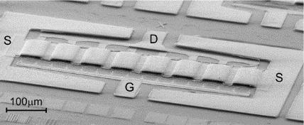
44 Device fabrication at IEMN within Inrel project Process flow: front side 1. Ohmic contacts Ti/Al based R C = 0.5 Ω.mm 2. Isolation by implantation 3. Gate module MIS configuration (MOCVD SiN as gate dielectric) Lg: 2 µm, W = 50 µm 4. SiN PECVD Passivation 5. Interconnects Front side SEM view of the GaN HEMT Typical blocking voltage about 1.2kV Transfer characteristics I D - V G Off-state characteristic of the GaN-on-Si HEMT with GD40
 Complete breakage of")
 as the strain issues will be significantly")
45 Device fabrication at IEMN within Inrel project Substrate removal on large area Image of large membranes (about 2 cm) Complete breakage of the membrane due to significant strain Substrate removal should be performed locally (mm 2 ) as the strain issues will be significantly reduced


46 Device fabrication at IEMN within Inrel project Process flow: backside 1. Wafer thinning and polishing down to 200 µm 2. Photolithography (laser writing) 3. Deep etching (Bosch process) High selectivity with the AlN nucleation layer G G resist Si GaN-based membrane


47 Backside view after local Si removal >50µm 200 µm Image of a 2x50 transistor GD20 backside view 500 µm Si Image of a multifingers transistor GD20 backside view Si
 while using a temperature deposition <")
48 UWBG such as AlN are a key to overcome vertical BV 16 µm AlN 4.5 µm 9.5 µm 16 µm High dielectric quality with a breakdown field much higher than GaN (> 4 MV/cm) while using a temperature deposition < 350 C Deposition by PVD can be achieved up to 12-inch: low cost


49 Comparison of electrical performances of GaN-on-Si vs. GaN-on-AlN 2x50 µm; GD: 40 µm; Lg : 2µm vs. Off-state characteristics (floating substrate) I D - V G of transistors on Si and on PVD AlN Very low leakage up to 3 kv (< 1 µa/mm)

50 Blocking voltage far beyond the state-of-the-art Lateral Breakdown 1 µa/mm Next step is to achieve these results on larger devices (> 10 mm)
51 o Introduction o Device design for high power devices o Description of the device fabrication o Main processing techniques o Main technological bricks o How to further push the breakdown limits of GaN-on-Si HEMTs o LSR approach developed within Inrel project o Conclusion


52 Future of microelectronics End of silicon domination, Introduction on the market of new materials such as high power GaN-on-Si for highly functional devices
53 Future of microelectronics Time for opportunities (new comers, young researcher or PhD students): Transition towards new materials Multidisciplinary research teams will be required to overcome future challenges Unlike niche applications such as microwave and mmw, the cost will remain the main figure of merit for next generation of power devices