EXCIMER LASER ANNEALING FOR LOW- TEMPERATURE POLYSILICON THIN FILM TRANSISTOR FABRICATION ON PLASTIC SUBSTRATES
|
|
|
- Godfrey Heath
- 6 years ago
- Views:
Transcription
1 EXCIMER LASER ANNEALING FOR LOW- TEMPERATURE POLYSILICON THIN FILM TRANSISTOR FABRICATION ON PLASTIC SUBSTRATES G. Fortunato, A. Pecora, L. Maiolo, M. Cuscunà, D. Simeone, A. Minotti, and L. Mariucci CNR-IMM, Roma, Italy
2 Outline Introduction Excimer laser annealing Device fabrication on plastic substrates TFTs characterization Conclusions
3 Introduction Low temperature Polysilicon (LTPS) TFT technology has attracted considerable interest over the last 20 years Introduction of excimer laser crystallization has considerably improved the device performances, allowing integration of CMOS circuitry along with active matrix switching elements LTPS TFTs represent key devices for large area electronics Active matrix LCDs Active matrix OLEDs System-on-glass (SOG) and system-on-plastic (SOP)


4 Flexible electronics Display Advertising Automotive Wearable Sensors Biomedical sensors Biomolecular detectors Radio-Frequency ID Tags (RFID) Lower production cost, lightness, transparency, robustness, rollable 3
 ppm/c 15 13 60-70 54 74 53 17 %Tr (400-700 nm) > 85 85 > 90 90 91.6 90 Yellow Water absorption (%) 0.14 0.14 0.2-0.4 1.4 0.03 0.4 1.8 Young s modulus/gpa 5.")
5 Polymeric substrates Polyethylene terephthalate (PET) Polyethylene naphthalate (PEN) Polycarbonate (PC) Polyethersulfone (PES) Polycyclic Olefin (PCO) Polyarylite (PAR) Polyimide (PI) Base polymer PET PEN PC PES PCO PAR PI CTE (-55 to 85 C) ppm/c %Tr ( nm) > > Yellow Water absorption (%) Young s modulus/gpa Tensile strength/mpa NA Tg C


6 LTPS TFTs issues low temperature process ELC active layer crystallization Excimer Laser Crystallization dielectrics ECR, ICP PECVD ECR 5
7 Excimer laser crystallization Combination in silicon of: strong UV absorption (α>10 6 cm -1 ) small heat diffusion length during laser pulse (~100 nm) Film melting without appreciable heating (<300 C) of the substrate Advantages of ELC process: glass and plastic compatible processing of large area substrates good crystallinity of polysilicon
8 Experimental set-up
9 Excimer laser crystallization partial melting almost complete melting (SLG) complete melting
 large non-uniformities Pulse-to-pulse fluctuations and non perfect beam homogenization prevent the opearation in this regime grain size (nm) 1200 1000 800 600 400 200 0")
10 Super Lateral Growth When few crystallites remain unmelted the grains can grow laterally (>1µm) Disadvantages of SLG regime: very narrow process window ( E/E SLG ~2.5%) large non-uniformities Pulse-to-pulse fluctuations and non perfect beam homogenization prevent the opearation in this regime grain size (nm) energy density


11 a-si precursor a-si precursor must contain low concentrations of H to perform excimer laser crystallization Conventional PECVD a-si:h, when deposited at 250 C, contains 8-12 at. % H Planar and X-TEM of a-si:h irradiated at RT (E d =190 mj/cm 2 )
12 Thermal de-hydrogenation Hydrogen can be removed by thermal treatments Two main peaks in the thermal desorption rate Typical treatments: C for a few hours
13 Laser de-hydrogenation It is possible to use laser annealing to de-hydrogenate the a-si:h film Large number of shots Combined with low-t thermal treatments E of final shot (mj/cm 2 ) Thick Si =100nm number of sequential shots


14 Excimer laser crystallization Fig.3 Fig.4 SEM and AFM images of 70 nm poly-si film after ELC at laser energy density of about 320mJ/cm 2 at 20 shots per point 6
 + laser annealing")
15 Polysilicon microstructure Sequential low-t thermal treatment (350 C) + laser annealing


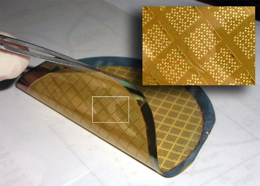
16 Device fabrication spin-coating of PI (HD-Microsistems 2611) onto 3 thermally oxidized Si-wafer and curing at a maximum temperature respectively of T= 350 C and T= 400 C, 8 µm thick PI film PI is mechanically separated from the carrier after device fabrication Easy handling, eliminate the problem of plastic shrinkage, allows the use of standard semiconductor equipment Mean surface roughness 3 nm 9
 for hydrogen removal 6.")
17 Non self-aligned TFT fabrication 1.Buffer layers: 200 nm Si 3 N 4 dual frequency 300 C 250 nm SiO C nm a-si:h by 300 C 3.25 nm n + by PECVD 4.s/d patterning and n + removal by selective wet etching 5.Furnace annealing 350 C and 400 C in N 2 (16 h) for hydrogen removal 6.p-Si formation and dopant activation by ELC 300mJ/cm 2 and 400mJ/cm 2 max) 7.Active layer island formation nm thick SiO 2 by ECR-PECVD at room temperature 9.Via-hole and metal contacts (s/d/g) C in N 2 (30 min) a-si SiO 2 Si 3 N 4 Polyimide c-si 10


18 AFM analysis Polysilicon grain sizes after excimer laser crystallization for two different dehydrogenation temperatures T=350 C E=300 mj/cm 2 T=400 C E=400 mj/cm nm 250 nm 11
19 Device fabrication 12
20 TFT electrical characterization I ds (A) Common features: Leakage < 1pA I on /I off > 10 6 V t = 6-8 V Optimal quality n + ohmic contact Sheet resistance about 600 Ω/ Low kink effect C V g (V) Semilog and linear scale TFTs transfer characteristics L=10 W= I ds (µa) I ds (µa) T=350 C: Field effect mobility = 40 cm 2 /Vs Subthreshold slope 1.2 V/dec T=400 C: Field effect mobility = 70 cm 2 /Vs Subthreshold slope 0.9 V/dec V g =8 V V g =9 V V g =10 V V ds (V) Output characteristics measured at increasing V g. (b) 13
21 Self-heating related instability 10-6 Transfer characteristics measured at V ds =0.1 V for increasing bias stressing times (bias stress at V g -V t =25 V and V ds =15 V) I ds (A) V g (V) No stressed 80 s 1280 s s Transfer characteristics measured at V ds =0.1 V at T=120 C for increasing stressing times (bias stress at V g -V t =25 V and V ds =0 V) I ds (A) No stressed 80 s 1280 s s V g (V) 14 L=20 µm W=40 µm

 Transfer characteristics for a")
22 Mechanical stress I ds (A) 1.2x x x x x10-7 L=10µm W=10µm Tensile Stress Compressive stress Flat 2.0x V g (V) Transfer characteristics for a poly-tft on PI under different mechanical stress with a R=1.3 cm 16
23 Conclusions A new process for LTPS TFTs fabrication on PI has been presented sample handling and plastic stability Excimer laser annealing was successfully applied for the crystallization of the active layer Better crystallinity was obtained when higher T thermal pre-treatments were performed The devices fabricated at higher temperature exhibited a field effect mobility up to 70 cm 2 /Vs Self-heating related instability of devices on plastic substrates could represent a serious issue and solutions are required The TFTs characteristics are not appreciably influenced by mechanical stress Acknowlegments This work has been partially supported by the project PLAST-Ics funded by the Italian Ministry for Research
Laser Crystallization for Low- Temperature Poly-Silicon (LTPS)
") Laser Crystallization for Low- Temperature Poly-Silicon (LTPS) David Grant University of Waterloo ECE 639 Dr. Andrei Sazonov What s the current problem in AM- LCD and large-area area imaging? a-si:h has
Laser Crystallization for Low- Temperature Poly-Silicon (LTPS) David Grant University of Waterloo ECE 639 Dr. Andrei Sazonov What s the current problem in AM- LCD and large-area area imaging? a-si:h has
Amorphous and Polycrystalline Thin-Film Transistors
 Part I Amorphous and Polycrystalline Thin-Film Transistors HYBRID AMORPHOUS AND POLYCRYSTALLINE SILICON DEVICES FOR LARGE-AREA ELECTRONICS P. Mei, J. B. Boyce, D. K. Fork, G. Anderson, J. Ho, J. Lu, Xerox
A Novel Low Temperature Self-Aligned Field Induced Drain Polycrystalline Silicon Thin Film Transistor by Using Selective Side-Etching Process
 Chapter 3 A Novel Low Temperature Self-Aligned Field Induced Drain Polycrystalline Silicon Thin Film Transistor by Using Selective Side-Etching Process 3.1 Introduction Low-temperature poly-si (LTPS) TFTs
Chapter 2 Manufacturing Process
 Digital Integrated Circuits A Design Perspective Chapter 2 Manufacturing Process 1 CMOS Process 2 CMOS Process (n-well) Both NMOS and PMOS must be built in the same silicon material. PMOS in n-well NMOS
Crystallization of Continuing Wave Laser Applications for Low-Temperature Polycrystalline Thin Film Transistors
 Chapter 4 Crystallization of Continuing Wave Laser Applications for Low-Temperature Polycrystalline Thin Film Transistors 4.1 Introduction Low temperature poly-silicon TFTs fabricated by excimer laser
DEVELOPMENTAL BIAXIALLY-ORIENTED PEEK FILM FOR FLEXBILE ELECTRONICS
 TECHNICAL PAPER DEVELOPMENTAL BIAXIALLY-ORIENTED PEEK FILM FOR FLEXBILE ELECTRONICS HIGH TEMPERATURE CAPABILITY, FLEXIBILITY AND STRENGTH Victrex plc www.victrex.com 2 Victrex Technical Paper SHAPING FUTURE
Defense Technical Information Center Compilation Part Notice
 UNCLASSIFIED Defense Technical Information Center Compilation Part Notice ADPO 11302 TITLE: A Novel Device Structure for Low-Temperature Polysilicon TFTs With Controlled Gain Growth in Channel Regions
Project III. 4: THIN FILM DEVICES FOR LARGE AREA ELECTRONICS
 Project III. 4: THIN FILM DEVICES FOR LARGE AREA ELECTRONICS Project leader: Dr D.N. Kouvatsos Collaborating researchers from other projects: Dr D. Davazoglou Ph.D. candidates: M. Exarchos, L. Michalas
Development of Silicon Pad and Strip Detector in High Energy Physics
 XXI DAE-BRNS High Energy Physics Symposium 2014, IIT Guwahati Development of Silicon Pad and Strip Detector in High Energy Physics Manoj Jadhav Department of Physics I.I.T. Bombay 2 Manoj Jadhav, IIT Bombay.
Czochralski Crystal Growth
 Czochralski Crystal Growth Crystal Pulling Crystal Ingots Shaping and Polishing 300 mm wafer 1 2 Advantage of larger diameter wafers Wafer area larger Chip area larger 3 4 Large-Diameter Wafer Handling
Silicon Epitaxial CVD Want to create very sharp PN boundary grow one type layer on other in single crystal form High dopant layers on low dopant
 Silicon Epitaxial CVD Want to create very sharp PN boundary grow one type layer on other in single crystal form High dopant layers on low dopant substrate Creates latch up protection for CMOS Buried Epi
Chapter 3 Silicon Device Fabrication Technology
 Chapter 3 Silicon Device Fabrication Technology Over 10 15 transistors (or 100,000 for every person in the world) are manufactured every year. VLSI (Very Large Scale Integration) ULSI (Ultra Large Scale
Polycrystalline Silicon Produced by Joule-Heating Induced Crystallization
 Polycrystalline Silicon Produced by Joule-Heating Induced Crystallization So-Ra Park 1,2, Jae-Sang Ro 1 1 Department of Materials Science and Engineering, Hongik University, Seoul, 121-791, Korea 2 EnSilTech
THIN FILM DEVICES for LARGE AREA ELECTRONICS
 Institute of Microelectronics Annual Report 2009 7 Project III. 3: THIN FILM DEVICES for LARGE AREA ELECTRONICS Project leader: Dr. D.N. Kouvatsos Collaborating researchers from other projects: Dr. D.
Microfabrication of Integrated Circuits
 Microfabrication of Integrated Circuits OUTLINE History Basic Processes Implant; Oxidation; Photolithography; Masks Layout and Process Flow Device Cross Section Evolution Lecture 38, 12/05/05 Reading This
Silicon Epitaxial CVD Want to create very sharp PN boundary grow one type layer on other in single crystal form High dopant layers on low dopant
 Silicon Epitaxial CVD Want to create very sharp PN boundary grow one type layer on other in single crystal form High dopant layers on low dopant substrate Creates latch up protection for CMOS Buried Epi
Polycrystalline Silicon Thin-Film Transistors Fabricated by Defect Reduction Methods
 IEEE TRANSACTIONS ON ELECTRON DEVICES, VOL. 49, NO. 12, DECEMBER 2002 2217 Polycrystalline Silicon Thin-Film Transistors Fabricated by Defect Reduction Methods H. Watakabe and T. Sameshima Abstract Fabrication
Microelettronica. Planar Technology for Silicon Integrated Circuits Fabrication. 26/02/2017 A. Neviani - Microelettronica
 Microelettronica Planar Technology for Silicon Integrated Circuits Fabrication 26/02/2017 A. Neviani - Microelettronica Introduction Simplified crosssection of an nmosfet and a pmosfet Simplified crosssection
Lecture #18 Fabrication OUTLINE
 Transistors on a Chip Lecture #18 Fabrication OUTLINE IC Fabrication Technology Introduction the task at hand Doping Oxidation Thin-film deposition Lithography Etch Lithography trends Plasma processing
Lecture #9: Active-Matrix LCDs
 Lecture #9: Active-Matrix LCDs Introduction OUTLINE Active-matrix switching elements TFT performance requirements Active matrix processing constraints Amorphous silicon (a-si) TFT technology TFT fabrication
Introduction to CMOS VLSI Design. Layout, Fabrication, and Elementary Logic Design
 Introduction to CMOS VLSI Design Layout, Fabrication, and Elementary Logic Design CMOS Fabrication CMOS transistors are fabricated on silicon wafer Lithography process similar to printing press On each
Ubiquitous Electronics:
 Ubiquitous Electronics: Why Now? Dollars per Megabit memory 100000 10000 1000 100 10 29% 1 Consumer 20% Consumer 0.1 Cost per megabit Transistors per Person 39% Consumer Form Factor Limiting Consumer Growth
Study on the hydrogenated ZnO-based thin film transistors
 Final Report Study on the hydrogenated ZnO-based thin film transistors To Dr. Gregg Jessen Asian Office of Aerospace Research & Development April 30th, 2011 Jae-Hyung Jang School of Information and Communications
EE40 Lec 22. IC Fabrication Technology. Prof. Nathan Cheung 11/19/2009
 Suggested Reading EE40 Lec 22 IC Fabrication Technology Prof. Nathan Cheung 11/19/2009 300mm Fab Tour http://www-03.ibm.com/technology/manufacturing/technology_tour_300mm_foundry.html Overview of IC Technology
Lecture 1A: Manufacturing& Layout
 Introduction to CMOS VLSI Design Lecture 1A: Manufacturing& Layout David Harris Harvey Mudd College Spring 2004 Steven Levitan Fall 2008 1 The Manufacturing Process For a great tour through the IC manufacturing
In 1966, the first polycrystalline silicon thin-film transistors (poly-si TFTs) were
 were") Chapter 1 Introduction In 1966, the first polycrystalline silicon thin-film transistors (poly-si TFTs) were fabricated by C. H. Fa et al. [1.1]. Since then, many investigations have been devoted to the
Chapter 1 Introduction In 1966, the first polycrystalline silicon thin-film transistors (poly-si TFTs) were fabricated by C. H. Fa et al. [1.1]. Since then, many investigations have been devoted to the
Complexity of IC Metallization. Early 21 st Century IC Technology
 EECS 42 Introduction to Digital Electronics Lecture # 25 Microfabrication Handout of This Lecture. Today: how are Integrated Circuits made? Silicon wafers Oxide formation by growth or deposition Other
PHYS 534 (Fall 2008) Process Integration OUTLINE. Examples of PROCESS FLOW SEQUENCES. >Surface-Micromachined Beam
 Process Integration OUTLINE. Examples of PROCESS FLOW SEQUENCES. >Surface-Micromachined Beam") PHYS 534 (Fall 2008) Process Integration Srikar Vengallatore, McGill University 1 OUTLINE Examples of PROCESS FLOW SEQUENCES >Semiconductor diode >Surface-Micromachined Beam Critical Issues in Process
PHYS 534 (Fall 2008) Process Integration Srikar Vengallatore, McGill University 1 OUTLINE Examples of PROCESS FLOW SEQUENCES >Semiconductor diode >Surface-Micromachined Beam Critical Issues in Process
Chapter 3 CMOS processing technology
 Chapter 3 CMOS processing technology (How to make a CMOS?) Si + impurity acceptors(p-type) donors (n-type) p-type + n-type => pn junction (I-V) 3.1.1 (Wafer) Wafer = A disk of silicon (0.25 mm - 1 mm thick),
Behavior of the parameters of microcrystalline silicon TFTs under mechanical strain. S. Janfaoui*, C. Simon, N. Coulon, T.
 Author manuscript, published in "Solid-State Electronics 93 (2014) 1-7" DOI : 10.1016/j.sse.2013.12.001 Behavior of the parameters of microcrystalline silicon TFTs under mechanical strain S. Janfaoui*,
CMOS Fabrication. Dr. Bassam Jamil. Adopted from slides of the textbook
 CMOS Fabrication Dr. Bassam Jamil Adopted from slides of the textbook CMOS Fabrication CMOS transistors are fabricated on silicon wafer Lithography process similar to printing press On each step, different
9/4/2008 GMU, ECE 680 Physical VLSI Design
 ECE680: Physical VLSI Design Chapter II CMOS Manufacturing Process 1 Dual-Well Trench-Isolated CMOS Process gate-oxide TiSi 2 AlCu Tungsten SiO 2 p-well poly n-well SiO 2 n+ p-epi p+ p+ 2 Schematic Layout
Excimer Laser Annealing of Hydrogen Modulation Doped a-si Film
 Materials Transactions, Vol. 48, No. 5 (27) pp. 975 to 979 #27 The Japan Institute of Metals Excimer Laser Annealing of Hydrogen Modulation Doped a-si Film Akira Heya 1, Naoto Matsuo 1, Tadashi Serikawa
Lecture 19 Microfabrication 4/1/03 Prof. Andy Neureuther
 EECS 40 Spring 2003 Lecture 19 Microfabrication 4/1/03 Prof. ndy Neureuther How are Integrated Circuits made? Silicon wafers Oxide formation by growth or deposition Other films Pattern transfer by lithography
EECS130 Integrated Circuit Devices
 EECS130 Integrated Circuit Devices Professor Ali Javey 9/13/2007 Fabrication Technology Lecture 1 Silicon Device Fabrication Technology Over 10 15 transistors (or 100,000 for every person in the world)
CRYSTALAS. UV Optics System for Excimer Laser Based Crystallization of Thin Silicon Films
 L A S E R S Y S T E M G M B H CRYSTALAS UV Optics System for Excimer Laser Based Crystallization of Thin Silicon Films CRYSTALAS The New Optical Crystallization System CRYSTALAS is an excimer laser-based
EE 5344 Introduction to MEMS. CHAPTER 3 Conventional Si Processing
 3. Conventional licon Processing Micromachining, Microfabrication. EE 5344 Introduction to MEMS CHAPTER 3 Conventional Processing Why silicon? Abundant, cheap, easy to process. licon planar Integrated
Yung-Hui Yeh, and Bo-Cheng Kung Display Technology Center (DTC), Industrial Technology Research Institute, Hsinchu 310, Taiwan
, Industrial Technology Research Institute, Hsinchu 310, Taiwan") Amorphous In 2 O 3 -Ga 2 O 3 -ZnO Thin Film Transistors and Integrated Circuits on Flexible and Colorless Polyimide Substrates Hsing-Hung Hsieh, and Chung-Chih Wu* Graduate Institute of Electronics Engineering,
Amorphous In 2 O 3 -Ga 2 O 3 -ZnO Thin Film Transistors and Integrated Circuits on Flexible and Colorless Polyimide Substrates Hsing-Hung Hsieh, and Chung-Chih Wu* Graduate Institute of Electronics Engineering,
TECHNOLOGY, PERFORMANCE AND DEGRADATION CHARACTERISTICS OF SLS ELA THIN FILM TRANSISTORS
 FACTA UNIVERSITATIS Series: Electronics and Energetics Vol. 26, N o 3, December 2013, pp. 247-280 DOI: 10.2298/FUEE1303247M TECHNOLOGY, PERFORMANCE AND DEGRADATION CHARACTERISTICS OF SLS ELA THIN FILM
Amorphous Oxide Transistor Electrokinetic Reflective Display on Flexible Glass
 Amorphous Oxide Transistor Electrokinetic Reflective Display on Flexible Glass Devin A. Mourey, Randy L. Hoffman, Sean M. Garner *, Arliena Holm, Brad Benson, Gregg Combs, James E. Abbott, Xinghua Li*,
Doping and Oxidation
 Technische Universität Graz Institute of Solid State Physics Doping and Oxidation Franssila: Chapters 13,14, 15 Peter Hadley Technische Universität Graz Institute of Solid State Physics Doping Add donors
Characterization and control of defect states of polycrystalline silicon thin film transistor fabricated by laser crystallization
 Journal of Non-Crystalline Solids 299 302 (2002) 1321 1325 www.elsevier.com/locate/jnoncrysol Characterization and control of defect states of polycrystalline silicon thin film transistor fabricated by
Large-Grain Polysilicon Films with Low Intragranular Defect Density by Low- Temperature Solid-Phase Crystallization
 Mat. Res. Soc. Symp. Proc. Vol. 715 2002 Materials Research Society Large-Grain Polysilicon Films with Low Intragranular Defect Density by Low- Temperature Solid-Phase Crystallization Xiang-Zheng Bo, Nan
Review of CMOS Processing Technology
 - Scaling and Integration Moore s Law Unit processes Thin Film Deposition Etching Ion Implantation Photolithography Chemical Mechanical Polishing 1. Thin Film Deposition Layer of materials ranging from
Surface Micromachining
 Surface Micromachining Micro Actuators, Sensors, Systems Group University of Illinois at Urbana-Champaign Outline Definition of surface micromachining Most common surface micromachining materials - polysilicon
Complementary Metal Oxide Semiconductor (CMOS)
") Technische Universität Graz Institute of Solid State Physics Complementary Metal Oxide Semiconductor (CMOS) Franssila: Chapters 26,28 Technische Universität Graz Institute of Solid State Physics Complementary
Technische Universität Graz Institute of Solid State Physics Complementary Metal Oxide Semiconductor (CMOS) Franssila: Chapters 26,28 Technische Universität Graz Institute of Solid State Physics Complementary
RECONFIGURABLE NEUROMORPHIC SYNAPSE INTERCONNECTS WITH TFT
 RECONFIGURABLE NEUROMORPHIC SYNAPSE INTERCONNECTS WITH TFT JAN GENOE PUBLIC Every neuron in a human brain is connected via its synapses to 10-15.000 other neurons. Those connections can be over time reconfigured
Micro-Electro-Mechanical Systems (MEMS) Fabrication. Special Process Modules for MEMS. Principle of Sensing and Actuation
 Fabrication. Special Process Modules for MEMS. Principle of Sensing and Actuation") Micro-Electro-Mechanical Systems (MEMS) Fabrication Fabrication Considerations Stress-Strain, Thin-film Stress, Stiction Special Process Modules for MEMS Bonding, Cavity Sealing, Deep RIE, Spatial forming
Micro-Electro-Mechanical Systems (MEMS) Fabrication Fabrication Considerations Stress-Strain, Thin-film Stress, Stiction Special Process Modules for MEMS Bonding, Cavity Sealing, Deep RIE, Spatial forming
Fabrication and Analysis of Carbon Doped Hydrogenated Amorphous Silicon Thin Film Transistors
 Microelectronics and Solid State Electronics 2016, 5(1): 14-18 DOI: 10.5923/j.msse.20160501.03 Fabrication and Analysis of Carbon Doped Hydrogenated Amorphous Silicon Thin Film Transistors T. K. Subramanyam,
CS/ECE 5710/6710. N-type Transistor. N-type from the top. Diffusion Mask. Polysilicon Mask. CMOS Processing
 CS/ECE 5710/6710 CMOS Processing Addison-Wesley N-type Transistor D G +Vgs + Vds S N-type from the top i electrons - Diffusion Mask Mask for just the diffused regions Top view shows patterns that make
行政院國家科學委員會補助專題研究計畫成果報告
 NSC89-2215-E-009-104 89 08 01 90 07 31 Fabrication and Characterization of Low-Temperature Polysilicon Thin Film Transistors with Novel Self-Aligned Sub-Gate Structures NSC89-2215-E009-104 (FID) self-aligned
Engineered Substrates
 Engineered Substrates Engineered Substrates Using the NanoCleave TM Process Francois J. Henley President and CEO Silicon Genesis Corporation San Jose, California SiGen Presentation Outline Engineered Substrates
Department of Electrical Engineering. Jungli, Taiwan
 Chapter 3 Fabrication of CMOS Integrated Circuits Jin-Fu Li Department of Electrical Engineering National Central University Jungli, Taiwan Background Outline The CMOS Process Flow Design Rules Latchup
Patterned heteroepitaxial SiGe thin films through. UV Excimer Laser radiation
 Patterned heteroepitaxial SiGe thin films through UV Excimer Laser radiation,, F.Gontad, J.C.Conde, E.Martín 1, A.Benedetti 2, C.Serra 2, J.Serra, P.González, B.León Departamento de Física Aplicada 1 Dpto.
High Mobility Flexible Amorphous IGZO Thin-Film Transistors with a Low Thermal Budget Ultra-Violet Pulsed Light Process.
 High Mobility Flexible Amorphous IGZO Thin-Film Transistors with a Low Thermal Budget Ultra-Violet Pulsed Light Process. M. Benwadih 1*, R. Coppard 1, K. Bonrad 2, A. Klyszcz 2, D. Vuillaume 3 1 : Univ.
CMOS FABRICATION. n WELL PROCESS
 CMOS FABRICATION n WELL PROCESS Step 1: Si Substrate Start with p- type substrate p substrate Step 2: Oxidation Exposing to high-purity oxygen and hydrogen at approx. 1000 o C in oxidation furnace SiO
Vacuum Deposition of High Performance Gas Barrier Materials for Electronics Applications
 Vacuum Deposition of High Performance Gas Barrier Materials for Electronics Applications Hélène Suttle DPhil Research Student Department of Materials -University of Oxford AIMCAL Fall Conference October
Physical Vapor Deposition (PVD) Zheng Yang
 Zheng Yang") Physical Vapor Deposition (PVD) Zheng Yang ERF 3017, email: yangzhen@uic.edu Page 1 Major Fabrication Steps in MOS Process Flow UV light Mask oxygen Silicon dioxide photoresist exposed photoresist oxide
Physical Vapor Deposition (PVD) Zheng Yang ERF 3017, email: yangzhen@uic.edu Page 1 Major Fabrication Steps in MOS Process Flow UV light Mask oxygen Silicon dioxide photoresist exposed photoresist oxide
M. Hasumi, J. Takenezawa, Y. Kanda, T. Nagao and T. Sameshima
 Proceedings of 6th Thin Film Materials & Devices Meeting November 2-3, 2009, Kyoto, Japan http://www.tfmd.jp/ Characterization of SiO x /Si Interface Properties by Photo Induced Carrier Microwave Absorption
Lect. 2: Basics of Si Technology
 Unit processes Thin Film Deposition Etching Ion Implantation Photolithography Chemical Mechanical Polishing 1. Thin Film Deposition Layer of materials ranging from fractions of nanometer to several micro-meters
FABRICATION OF CMOS INTEGRATED CIRCUITS. Dr. Mohammed M. Farag
 FABRICATION OF CMOS INTEGRATED CIRCUITS Dr. Mohammed M. Farag Outline Overview of CMOS Fabrication Processes The CMOS Fabrication Process Flow Design Rules EE 432 VLSI Modeling and Design 2 CMOS Fabrication
VLSI INTRODUCTION P.VIDYA SAGAR ( ASSOCIATE PROFESSOR) Department of Electronics and Communication Engineering, VBIT
 Department of Electronics and Communication Engineering, VBIT") VLSI INTRODUCTION P.VIDYA SAGAR ( ASSOCIATE PROFESSOR) contents UNIT I INTRODUCTION: Introduction to IC Technology MOS, PMOS, NMOS, CMOS & BiCMOS technologies. BASIC ELECTRICAL PROPERTIES : Basic Electrical
VLSI INTRODUCTION P.VIDYA SAGAR ( ASSOCIATE PROFESSOR) contents UNIT I INTRODUCTION: Introduction to IC Technology MOS, PMOS, NMOS, CMOS & BiCMOS technologies. BASIC ELECTRICAL PROPERTIES : Basic Electrical
Response surface optimization for high-performance solid-phase crystallized silicon-germanium thin film transistors
 Response surface optimization for high-performance solid-phase crystallized silicon-germanium thin film transistors Vivek Subramanian a, Krishna Saraswat a, Howard Hovagimian b, and John Mehlhaff b a Electrical
Sputtering Target of Oxide Semiconductor with High Electron Mobility and High Stability for Flat Panel Displays
 ELECTRONICS Sputtering Target of Oxide Semiconductor with High Electron Mobility and High Stability for Flat Panel Displays Miki MIYANAGA*, Kenichi WATATANI, and Hideaki AWATA ----------------------------------------------------------------------------------------------------------------------------------------------------------------------------------------------------------------------------------------------------------
Problem 1 Lab Questions ( 20 points total)
") Problem 1 Lab Questions ( 20 points total) (a) (3 points ) In our EE143 lab, we use Phosphorus for the source and drain diffusion. However, most advanced processes use Arsenic. What is the advantage of
Problem 1 Lab Questions ( 20 points total) (a) (3 points ) In our EE143 lab, we use Phosphorus for the source and drain diffusion. However, most advanced processes use Arsenic. What is the advantage of
MICROCHIP MANUFACTURING by S. Wolf
 MICROCHIP MANUFACTURING by S. Wolf Chapter 7: BASICS OF THIN FILMS 2004 by LATTICE PRESS Chapter 7: Basics of Thin Films CHAPTER CONTENTS Terminology of Thin Films Methods of Thin-Film Formation Stages
2-1 Introduction The demand for high-density, low-cost, low-power consumption,
 Chapter 2 Hafnium Silicate (HfSi x O y ) Nanocrystal SONOS-Type Flash Memory Fabricated by Sol-Gel Spin Coating Method Using HfCl 4 and SiCl 4 as Precursors 2-1 Introduction The demand for high-density,
Fabrication and Layout
 ECEN454 Digital Integrated Circuit Design Fabrication and Layout ECEN 454 3.1 A Glimpse at MOS Device Polysilicon Aluminum ECEN 475 4.2 1 Material Classification Insulators Glass, diamond, silicon oxide
This Appendix discusses the main IC fabrication processes.
 IC Fabrication B B.1 Introduction This Appendix discusses the main IC fabrication processes. B.2 NMOS fabrication NMOS transistors are formed in a p-type substrate. The NMOS fabrication process requires
LOW-TEMPERATURE poly-si (LTPS) thin-film transistors
 thin-film transistors") IEEE TRANSACTIONS ON ELECTRON DEVICES, VOL. 51, NO. 1, JANUARY 2004 63 Performance and Reliability of Low-Temperature Polysilicon TFT With a Novel Stack Gate Dielectric and Stack Optimization Using PECVD
IEEE TRANSACTIONS ON ELECTRON DEVICES, VOL. 51, NO. 1, JANUARY 2004 63 Performance and Reliability of Low-Temperature Polysilicon TFT With a Novel Stack Gate Dielectric and Stack Optimization Using PECVD
Roll-to-roll Vacuum Processing of Organic Thin Film Transistors
 Roll-to-roll Vacuum Processing of Organic Thin Film Transistors Hazel Assender Department of Materials University of Oxford DALMATIAN TECHNOLOGY 1 Aim of the Research To demonstrate the ability to fabricate
Introduction. 1. Sputtering process, target materials and their applications
 Sputtering is widely used in the production of electronic devices such as liquid crystal displays (LCDs), optical media, magnetic media and semiconductors. The Kobelco Research Institute, Inc. has been
Chapter 3. In this chapter, we use sol-gel method to combine three high-k precursors, i.e. HfCl 4, ZrCl 4 and SiCl 4 together to form hafnium silicate
 Chapter 3 Sol-Gel-Derived Zirconium Silicate (ZrSi x O y ) and Hafnium Silicate (HfSi x O y ) Co-existed Nanocrystal SONOS Memory 3-1 Introduction In the previous chapter, we fabricate the sol-gel-derived
Development and modeling of a low temperature thin-film CMOS on glass
 Rochester Institute of Technology RIT Scholar Works Theses Thesis/Dissertation Collections 2-6-2009 Development and modeling of a low temperature thin-film CMOS on glass Robert G. Manley Follow this and
Microstructure of Electronic Materials. Amorphous materials. Single-Crystal Material. Professor N Cheung, U.C. Berkeley
 Microstructure of Electronic Materials Amorphous materials Single-Crystal Material 1 The Si Atom The Si Crystal diamond structure High-performance semiconductor devices require defect-free crystals 2 Crystallographic
Characteristics of HfO 2 pmosfet with Ultrashallow Junction Prepared by Plasma Doping and Laser Annealing
 Characteristics of HfO 2 pmosfet with Ultrashallow Junction Prepared by Plasma Doping and Laser Annealing Sungkweon Baek, Sungho Heo, and Hyunsang Hwang Dept. of Materials Science and Engineering Kwangju
Interconnects. Outline. Interconnect scaling issues Aluminum technology Copper technology. Properties of Interconnect Materials
 Interconnects Outline Interconnect scaling issues Aluminum technology Copper technology 1 Properties of Interconnect Materials Metals Silicides Barriers Material Thin film Melting resistivity point ( C)
IC/MEMS Fabrication - Outline. Fabrication
 IC/MEMS Fabrication - Outline Fabrication overview Materials Wafer fabrication The Cycle: Deposition Lithography Etching Fabrication IC Fabrication Deposition Spin Casting PVD physical vapor deposition
Lecture 2: CMOS Fabrication Mark McDermott Electrical and Computer Engineering The University of Texas at Austin
 Lecture 2: CMOS Fabrication Mark McDermott Electrical and Computer Engineering The University of Texas at Austin Agenda Last module: Introduction to the course How a transistor works CMOS transistors This
Amorphous silicon / crystalline silicon heterojunction solar cell
 Workshop on "Physics for Renewable Energy" October 17-29, 2005 301/1679-9 "Amorphous Silicon / Cyrstalline Silicon Heterojunction Solar Cell" E. Centurioni CNR/IMM AREA Science Park - Bologna Italy Amorphous
Properties of Inclined Silicon Carbide Thin Films Deposited by Vacuum Thermal Evaporation
 182 Properties of Inclined Silicon Carbide Thin Films Deposited by Vacuum Thermal Evaporation Oday A. Hamadi, Khaled Z. Yahia, and Oday N. S. Jassim Abstract In this work, thermal evaporation system was
Chapter 2 MOS Fabrication Technology
 Chapter 2 MOS Fabrication Technology Abstract This chapter is concerned with the fabrication of metal oxide semiconductor (MOS) technology. Various processes such as wafer fabrication, oxidation, mask
UT Austin, ECE Department VLSI Design 2. CMOS Fabrication, Layout Rules
 2. CMOS Fabrication, Layout, Design Rules Last module: Introduction to the course How a transistor works CMOS transistors This module: CMOS Fabrication Design Rules CMOS Fabrication CMOS transistors are
Fabrication Technology
 Fabrication Technology By B.G.Balagangadhar Department of Electronics and Communication Ghousia College of Engineering, Ramanagaram 1 OUTLINE Introduction Why Silicon The purity of Silicon Czochralski
CMOS Technology. Flow varies with process types & company. Start with substrate selection. N-Well CMOS Twin-Well CMOS STI
 CMOS Technology Flow varies with process types & company N-Well CMOS Twin-Well CMOS STI Start with substrate selection Type: n or p Doping level, resistivity Orientation, 100, or 101, etc Other parameters
Fabrication Techniques for Thin-Film Silicon Layer Transfer
 Fabrication Techniques for Thin-Film Silicon Layer Transfer S. L. Holl a, C. A. Colinge b, S. Song b, R. Varasala b, K. Hobart c, F. Kub c a Department of Mechanical Engineering, b Department of Electrical
EE BACKEND TECHNOLOGY - Chapter 11. Introduction
 1 EE 212 FALL 1999-00 BACKEND TECHNOLOGY - Chapter 11 Introduction Backend technology: fabrication of interconnects and the dielectrics that electrically and physically separate them. Aluminum N+ Early
Growth and Doping of SiC-Thin Films on Low-Stress, Amorphous Si 3 N 4 /Si Substrates for Robust Microelectromechanical Systems Applications
 Journal of ELECTRONIC MATERIALS, Vol. 31, No. 5, 2002 Special Issue Paper Growth and Doping of SiC-Thin Films on Low-Stress, Amorphous Si 3 N 4 /Si Substrates for Robust Microelectromechanical Systems
A Nano-thick SOI Fabrication Method
 A Nano-thick SOI Fabrication Method C.-H. Huang 1, J.T. Cheng 1, Y.-K. Hsu 1, C.-L. Chang 1, H.-W. Wang 1, S.-L. Lee 1,2, and T.-H. Lee 1,2 1 Dept. of Mechanical Engineering National Central University,
Effective Annealing and Crystallization of Si Film for Advanced TFT System
 Journal of Information Display, Vol. 11, No. 1, March 2010 (ISSN 1598-0316) 2010 KIDS Effective Annealing and Crystallization of Si Film for Advanced TFT System Takashi Noguchi Abstract The effect of the
ECSE-6300 IC Fabrication Laboratory Lecture 4: Dielectrics and Poly-Si Deposition. Lecture Outline
 ECSE-6300 IC Fabrication Laboratory Lecture 4: Dielectrics and Poly-Si Deposition Prof. Rensselaer Polytechnic Institute Troy, NY 12180 Office: CII-6229 Tel.: (518) 276-2909 e-mails: luj@rpi.edu http://www.ecse.rpi.edu/courses/s18/ecse
All fabrication was performed on Si wafers with 285 nm of thermally grown oxide to
 Supporting Information: Substrate preparation and SLG growth: All fabrication was performed on Si wafers with 285 nm of thermally grown oxide to aid in visual inspection of the graphene samples. Prior
Total Points = 110 possible (graded out of 100)
") Lab Report 1 Table of Contents 1. Profiles & Layout (9 Points) 2. Process Procedures (20 points) 3. Calculations (36 Points) 4. Questions (35 Points) 5. Bonus Questions (10 Points) Total Points = 110 possible
Lab Report 1 Table of Contents 1. Profiles & Layout (9 Points) 2. Process Procedures (20 points) 3. Calculations (36 Points) 4. Questions (35 Points) 5. Bonus Questions (10 Points) Total Points = 110 possible
Chapter 2. Density 2.65 g/cm 3 Melting point Young s modulus Tensile strength Thermal conductivity Dielectric constant 3.
 Chapter 2 Thin Film Materials Thin films of Silicon dioxide, Silicon nitride and Polysilicon have been utilized in the fabrication of absolute micro pressure sensor. These materials are studied and discussed
Low Temperature Dielectric Deposition for Via-Reveal Passivation.
 EMPC 2013, September 9-12, Grenoble; France Low Temperature Dielectric Deposition for Via-Reveal Passivation. Kath Crook, Mark Carruthers, Daniel Archard, Steve Burgess, Keith Buchanan SPTS Technologies,
Welcome MNT Conference 1 Albuquerque, NM - May 2010
 Welcome MNT Conference 1 Albuquerque, NM - May 2010 Introduction to Design Outline What is MEMs Design General Considerations Application Packaging Process Flow What s available Sandia SUMMiT Overview
VLSI Design and Simulation
 VLSI Design and Simulation CMOS Processing Technology Topics CMOS Processing Technology Semiconductor Processing How do we make a transistor? Fabrication Process Wafer Processing Silicon single crystal
Low temperature amorphous and nanocrystalline silicon thin film transistors. deposited by Hot-Wire CVD on glass substrate
 Low temperature amorphous and nanocrystalline silicon thin film transistors deposited by Hot-Wire CVD on glass substrate M. Fonrodona 1, D. Soler 1, J. Escarré 1, F. Villar 1, J. Bertomeu 1 and J. Andreu
Supplementary Figure S1 Photograph of MoS 2 and WS 2 flakes exfoliated by different metal naphthalenide (metal = Na, K, Li), and dispersed in water.
, and dispersed in water.") Supplementary Figure S1 Photograph of MoS 2 and WS 2 flakes exfoliated by different metal naphthalenide (metal = Na, K, Li), and dispersed in water. Supplementary Figure S2 AFM measurement of typical LTMDs
Supplementary Figure S1 Photograph of MoS 2 and WS 2 flakes exfoliated by different metal naphthalenide (metal = Na, K, Li), and dispersed in water. Supplementary Figure S2 AFM measurement of typical LTMDs
VLSI Systems and Computer Architecture Lab
 ΚΥΚΛΩΜΑΤΑ VLSI Πανεπιστήμιο Ιωαννίνων CMOS Technology Τμήμα Μηχανικών Η/Υ και Πληροφορικής 1 From the book: An Introduction ti to VLSI Process By: W. Maly ΚΥΚΛΩΜΑΤΑ VLSI Διάρθρωση 1. N well CMOS 2. Active