MODEL SEM Mill. Two independently adjustable TrueFocus ion sources
|
|
|
- Grace Pitts
- 6 years ago
- Views:
Transcription
1
 samples for a wide variety of applications.")
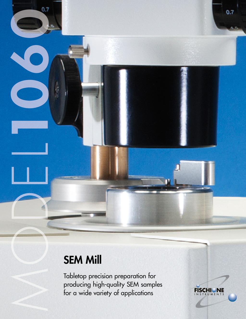
2 MODEL 1060 SEM Mill A state-of-the-art ion milling and polishing system. It is compact, precise, and consistently produces high-quality scanning electron microscopy (SEM) samples for a wide variety of applications. Two independently adjustable TrueFocus ion sources High energy operation for rapid milling; low energy operation for sample polishing Adjustable beam diameters ION MILLING Ion milling is used in the physical sciences to enhance the sample s surface characteristics. Inert gas, typically argon, is ionized and then accelerated toward the sample surface. By means of momentum transfer, the impinging ions sputter material from the sample at a controlled rate. Simple setup of milling parameters Individual, automatic ion source gas control Continuously adjustable milling angle range of 0 to +10 Sample rocking or rotation Stereo microscope for direct sample observation High-magnification microscope and CCD camera Basic and premium editions available (basic edition shown at left)

3 Advanced sample preparation For many of today s advanced materials, analysis by SEM is an ideal technique for rapidly studying material structure and properties. Fischione Model 1060 SEM Mill is an excellent tool for creating the sample surface characteristics needed for SEM imaging and analysis. Two ion sources Two TrueFocus ion sources direct controlleddiameter ion beams to the surface of the sample. Beam diameter is user adjustable. Both sources are concentrated on the sample surface for high milling rates. The ion Ion accelerating voltages can be varied from 6.0 kev for rapid milling to 100 ev for final sample polishing sources are physically small and require minimal gas but deliver a large range of ion beam energies. When operated in the upper energy range, milling is rapid, even at low angles. When operated at low energy, material is gradually sputtered from the sample without inducing artifacts. The unique design of the TrueFocus ion source allows for a controlled ion beam diameter, which means the ions are directed only to the sample and sputtered material is not redeposited from the sample holder and/or chamber onto the sample surface. Ion accelerating voltages are programmable and can be continuously varied from as high as 6.0 kev for rapid milling to as low as 100 ev for final sample polishing. Ion beam currents can be established from hundreds of nanoamperes to tens of microamperes. The SEM Mill is equipped with Faraday cups for measuring ion beam current. The ion sources are visually aligned from outside the vacuum using a luminescent target. Automatic gas control Two mass-flow controllers provide independent and automatic regulation of process gas for the ion sources. The gas control algorithm produces stable ion beams over a wide variety of ion source milling parameters. Fully integrated dry vacuum system The fully integrated vacuum system includes a turbomolecular drag pump backed by a multi-stage diaphragm pump. This oil-free system assures a clean environment for sample processing. Because the gas requirements of the TrueFocus ion source are small, the 70 lps turbomolecular Premium edition Model 1060 SEM Mill shown fully equipped 3


4 Examples of the various sample holders available for the Model 1060 SEM Mill drag pump produces an operating system vacuum of approximately 5x10⁻⁴ mbar. The vacuum level is measured with a Pirani gauge and is continuously indicated. Sample mounting and positioning The SEM Mill accommodates a wide range of sample sizes and configurations for applications such as bulk milling, electron backscatter diffraction (EBSD), semiconductor preparation, as well as traditional slope cutting and crosssectional polishing. A series of sample holders are available for a multitude of applications. Loading stations further facilitate the sample handling process. Chamber The SEM Mill s vacuum chamber remains under continuous vacuum during operation. A load lock isolates the high chamber vacuum from ambient during sample exchange, ensuring optimal vacuum conditions. The small chamber size makes it easy to clean during periodic maintenance. Quick sample transfer The SEM Mill s vacuum chamber remains under continuous vacuum during operation. A load lock isolates the high chamber vacuum from ambient during sample exchange, ensuring optimal vacuum conditions. The small chamber size makes it easy to clean during periodic maintenance. Cold trap (optional) The SEM Mill is available with an optional cold trap that is highly effective in removing hydrocarbons and water vapor therefore improving the chamber vacuum quality. The cold trap features a dewar located within the enclosure. Precise angle adjustment With the sample stage fixed in position, the ion sources are tilted to provide the desired milling angle. Tilt angles are continuously adjustable in the range from 0 to +10. Ion beam impingement angles are independently adjustable for each ion source. 4
5 Ion milling with low angles of incidence (less than 10 ), combined with low-energy ion source operation, minimizes irradiation damage and sample heating. Because it facilitates the uniform thinning of dissimilar materials, low-angle milling is highly beneficial when preparing layered or composite materials as well as crosssectional SEM samples. Programmable specimen motion Sample rotation is in-plane and continuous throughout 360. The SEM Mill is ideally suited to preparing cross-sectional samples from heterogeneous or layered materials. Sample holders are indexed to the sample stage for repeatable orientation and stage rotation speed (rotations per minute) is user adjustable. Sample motion control in relation to the ion beam minimizes preferential milling, which can occur when a glue bond line exists in cross sectional samples or when lower atomic number (Z) materials are contained in layered composite samples. In addition, the sample can be rocked in relation to the ion beam so that interfaces or glue lines are never parallel to the direction of the ion beam. Rocking angles ranging from ±40 to ±60 are typically employed. Automatic termination The ion milling process can be automatically terminated by elapsed time. A timer allows milling to continue for a predetermined time, and then turns off the power to the ion sources while keeping the sample under vacuum until the user vents the load lock to extract the sample. A sample can be serial sectioned by applying subsequent milling steps using the same parameters for the same time duration. Sample viewing The viewing window is protected by a shutter which prevents buildup of sputtered material that could interfere with sample observation. A light source located above the sample surface is used for illumination. Stereo microscope (optional) The SEM Mill accepts a stereo microscope to enhance sample viewing. The microscope s long working distance allows the sample to be observed in situ while milling. High magnification microscope (optional) The SEM Mill can be configured with an imaging system including a high-magnification microscope coupled to a CCD camera and video monitor to capture and display images. This system is ideal for preparing site-specific samples. When the high-magnification microscope and CCD camera are used, the sample is brought into the load lock for image capture and then returned to the milling position to continue the milling process. Instrument operation The SEM Mill features a universal control platform that manages total instrument operation. The basic edition of the SEM Mill is for users who require only primary level instrumentation function. The premium edition of the SEM Mill adds full computer control for setting, operating, and recording a broad variety of instrument parameters. Basic edition The basic edition is programmed via a touch screen embedded module. Initially, milling angles are established by manually positioning the ion sources to their desired orientations. A single-step recipe of parameters including ion beam energy, sample motion, sample position (load lock or milling), and process time is then readily programmed through the touch screen. Once the user initiates the process, the instrument automatically executes the recipe and continuously displays the real-time milling conditions. 5


6 The Operator Console application user interface is available only on the premium edition Model 1060 SEM Mill. Premium edition The premium edition is connected to a dedicated computer to provide enhanced programming capabilities and an expanded interface, thus minimizing the need for user intervention during the milling process. The interface facilitates programming of ion beam energy, milling angle, sample motion, sample position, and process time. For effective, unattended operation, a series of operational sequences can be established. Typical methodology starts with rapid milling; then a slower milling rate is employed to eliminate artifacts. Milling recipes can readily be stored and recalled. Advanced functionality includes structured management of sample data, image acquisition and storage, maintenance and log files, as well as remote access and diagnostics. The touch screen user interface is available on both basic and premium edition Model 1060 SEM Mills. The software allows secure access to the various instrument controls corresponding to levels of user expertise and needs for instrument operation. 6
7 Administrative rights can be provided to qualified maintenance staff. During operation, relevant parameters are displayed in real time on the computer monitor. When controlled by the computer, the touchscreen displays a Pause button so that, if necessary, instrument operation can be quickly suspended. The premium edition has the optional capability of remote monitoring via a network connection. This allows the instrument to be both monitored and paused remotely. Multiple SEM Mills can be networked. Applications The SEM Mill is an excellent tool for removing surface artifacts from SEM samples leading to improved imaging and analysis. SEM samples are frequently prepared by metallographic polishing. Often, an unwanted topography remains, even when great care is taken during the preparation process. With today s advanced SEMs, even a minimal amount of damage may limit the ability to fully resolve or analyze the surface of a sample. Sputtering material from the sample surface with inert gas ion beam milling is an ideal method to remove prior damage. This is the basis for the SEM Mill. Bulk Virtually any type of inorganic SEM sample can benefit from treatment with the SEM Mill. When the ion beams are directed at low incidence angles, layers containing residual mechanical damage, oxidation or contamination are sputtered away, yielding a pristine surface for SEM imaging and analysis. EBSD EBSD is a useful technique in which crystallographic information is obtained with a SEM because backscattered electrons form a pattern that represents the material s crystalline structure, orientation, and texture. Because EBSD is a highly surface-sensitive technique, any type of damage limits the ability to generate a pattern or to determine useful information from the pattern. Therefore, enhancing the surface with the SEM Mill is highly beneficial. To take EBSD to the next level, the SEM Mill can be used to remove precise and repeatable amounts of material from the sample. This serial sectioning technique yields information that may not be evident when using two-dimensional methods. Cross sectional semiconductor In many cases in the semiconductor industry, SEM allows information to be rapidly generated for applications such as failure analysis where it is essential to obtain useful data quickly. Frequently, the sample is prepared by cleaving or mechanical polishing that causes surface damage. Such damage is readily removed by ion milling with the SEM Mill. Dedicated sample holders facilitate the process. Minimal maintenance Material sputtered from the ion source is negligible, minimizing both sample contamination and component maintenance. Automated shuttering prevents the buildup of sputtered material on the viewing window. All system components are easily accessible for routine cleaning and maintenance. When connected to the Internet, the SEM Mill can be accessed remotely for diagnostic purposes. 7
8 Basic vs. premium edition feature comparison Feature Basic Edition Premium Edition Touch screen control Computer control Single-step recipe Multiple-step recipe Recipe storage and recall Real-time milling conditions display Automatic height sensing Manual milling angle adjustment Automated milling angle adjustment Independent ion source voltage control * Unattended operation Image capture * Maintenance and log files Remote access and process monitoring (single or multiple SEM Mills) Remote diagnostics * * Optional E.A. Fischione Instruments, Inc Corporate Circle Export, PA USA Tel: Fax: info@fischione.com E.A. Fischione Instruments, Inc. All rights reserved. Patents pending. Document Number PB1060 Revision 01 09/2013
MODEL TEM Mill. Two independently adjustable TrueFocus ion sources
 MODEL 1050 TEM Mill A state-of-the-art ion milling and polishing system. It is compact, precise, and consistently produces high-quality transmission electron microscopy (TEM) specimens with large electron
Model TEM Mill. Tabletop precision preparation for producing high-quality TEM specimens from a wide variety of materials EXCELLENCE MAGNIFIED
 Model 1050 TEM Mill Tabletop precision preparation for producing high-quality TEM specimens from a wide variety of materials EXCELLENCE MAGNIFIED Modular design for basic instrument operation or fully
MODEL 1051 TEM Mill ION MILLING. Ion milling is used on physical science. specimens to reduce thickness to electron
 MODEL 1051 TEM Mill A state-of-the-art ion milling and polishing system offering reliable, high performance specimen preparation. It is compact, precise, and consistently produces high-quality transmission
MODEL 1061 SEM Mill ION MILLING. Ion milling is used in the physical. sciences to enhance the sample s surface. characteristics. Inert gas, typically
 MODEL 1061 SEM Mill A state-of-the-art ion milling and polishing system. It is compact, precise, and consistently produces high-quality scanning electron microscopy (SEM) samples in the shortest amount
MODEL NanoMill TEM Specimen Preparation System. Ultra-low-energy, inert-gas ion source. Concentrated ion beam with scanning capabilities
 MODEL 1040 NanoMill TEM Specimen Preparation System The NanoMill system uses an ultra-low energy, concentrated ion beam to produce the highest quality specimens for transmission electron microscopy. Ultra-low-energy,
MODEL PicoMill TEM specimen preparation system. Achieve ultimate specimen quality free from amorphous and implanted layers
 MODEL 1080 PicoMill TEM specimen preparation system Combines an ultra-low energy, inert gas ion source, and a scanning electron column with multiple detectors to yield optimal TEM specimens. POST-FIB PROCESSING
MODEL Plasma Cleaner. Simultaneously cleans specimen and specimen holder. Cleans highly contaminated specimens in 2 minutes or less
 MODEL 1020 Plasma Cleaner Cleans specimens immediately before they are inserted into the electron microscope; removes existing carbonaceous debris from the specimen and prevents contamination from occurring
Specimen configuration
 APPLICATIONNOTE Model 1040 NanoMill TEM specimen preparation system Specimen configuration Preparing focused ion beam (FIB) milled specimens for submission to Fischione Instruments. The Model 1040 NanoMill
Model Plasma Cleaner. Effectively cleans specimens for electron microscopy EXCELLENCE MAGNIFIED
 Model 1020 Plasma Cleaner Effectively cleans specimens for electron microscopy EXCELLENCE MAGNIFIED Model 1020 Plasma Cleaner Simultaneously cleans specimen and specimen holder. Cleans highly contaminated
 LA-UR-01-3685 Approved for public release; distribution is unlimited. Title: USING A MULTI-DISCIPLINARY APPROACH, THE FIRST ELECTRON BACKSCATTERED KIKUCHI PATTERNS WERE CAPTURED FOR A PLUTONIUM ALLOY Author(s):
BAF 060 Freeze-Fracture System
 BAL-TEC AG EM-TECHNOLOGY AND APPLICATION BAF 060 GRE BAF 060 Freeze-Fracture System 20.05.99 Internet: www.bal-tec.com 1 / 6 BAF 060 - Designed to meet your needs Load-Lock Transfer of Specimen: For fast
In-situ Heating Characterisation Using EBSD
 Webinar In-situ Heating Characterisation Using EBSD Speakers Dr. Ali Gholinia Dr. Neil Othen Dr. Jenny Goulden Topics Introduction to EBSD Why do in-situ experiments? EBSD equipment requirements for in-situ
Power Vision Ltd. PV Research. Power Vision Ltd. Unit R2, Herald Park, Crewe, Cheshire, CW1 6EA, UK Tel:
 Power Vision Ltd PV Research Power Vision Ltd Unit R2, Herald Park, Crewe, Cheshire, CW1 6EA, UK www.pvoptical.com Tel: +44 1270 253000 Flexible Whether it be fast AR coating onto temperature sensitive
JSM-7800F Field Emission Scanning Electron Microscope
 JSM-7800F catalogue JSM-7800F Field Emission Scanning Electron Microscope We provide high performance The Ultimate Research Tool for Multi-Disciplinary Research Institutions Extreme resolution The super
IBS/e Ion Beam Sputter Deposition and Etching System. IBS/e with KDC-10 Ion Beam Sputter Deposition and Etching System with Kaufman Ion Source
 IBS/e Ion Beam Sputter Deposition and Etching System IBS/e with KDC-10 Ion Beam Sputter Deposition and Etching System with Kaufman Ion Source The Model IBS/e is a high vacuum thin film deposition system
Transzmissziós és pásztázó elektronmikroszkópos minták készítése ionsugaras vékonyítással
 Transzmissziós és pásztázó elektronmikroszkópos minták készítése ionsugaras vékonyítással Radi Zsolt Technoorg Linda Kft., Budapest Oktatói és Doktorandusz Konferencia Visegrád, 2012 State-of-the-art materials
Thermo Scientific ARL EQUINOX X-ray Diffractometers
 Thermo Scientific ARL EQUINOX 1000 X-ray Diffractometers High performance in a compact size Thermo Scientific ARL EQUINOX 1000 X-ray diffractometer (XRD) is designed to meet structural and phase analysis
Specimen Preparation Technique for a Microstructure Analysis Using the Focused Ion Beam Process
 Specimen Preparation Technique for a Microstructure Analysis Using the Focused Ion Beam Process by Kozue Yabusaki * and Hirokazu Sasaki * In recent years the FIB technique has been widely used for specimen
METHOD FOR IMPROVING FIB PREPARED TEM SAMPLES BY VERY LOW ENERGY Ar + ION MILL POLISHING
 METHOD FOR IMPROVING FIB PREPARED TEM SAMPLES BY VERY LOW ENERGY Ar + ION MILL POLISHING Yaron Kauffmann, Tzipi Cohen-Hyams, Michael Kalina, Hila Sadan-Meltzman and Wayne D. Kaplan Dept. of Materials Engineering
Q150R Series Rotary Pumped Coaters
 Q u o r u m Te c h n ologies Q150R Modular Coating Systems Q Series Rotary Pumped Coating Systems Innovative and versatile sputter High vacuum sputtering and carbon coater and carbonfor evaporator evaporation
A STUDY OF THE EFFECTIVENESS OF THE REMOVAL OF HYDROCARBON CONTAMINATION BY OXIDATIVE CLEANING INSIDE THE SEM.
 A STUDY OF THE EFFECTIVENESS OF THE REMOVAL OF HYDROCARBON CONTAMINATION BY OXIDATIVE CLEANING INSIDE THE SEM. Neal Sullivan, Tung Mai, Scott Bowdoin* and Ronald Vane** A poster paper presented at Microscopy
Observation in the GB (Gentle Beam) Capabilities
 Capabilities") A field-emission cathode in the electron gun of a scanning electron microscope provides narrower probing beams at low as well as high electron energy, resulting in both improved spatial resolution and
A field-emission cathode in the electron gun of a scanning electron microscope provides narrower probing beams at low as well as high electron energy, resulting in both improved spatial resolution and
Thermo Scientific ARL EQUINOX 100. X-ray Diffractometers
 Thermo Scientific ARL EQUINOX 100 X-ray Diffractometers High performance in a compact size Thermo Scientific ARL EQUINOX 100 X-ray diffractometer (XRD) is designed to meet structural and phase analysis
Si DRIE APPLICATION In Corial 210IL
 Si DRIE APPLICATION In Corial 210IL CORIAL 210IL ICP-RIE equipment for deep Si etching applications Enlarged functionality with capability to deep etch silicon, silicon carbide, glass, sapphire, and quartz
ATTACHMENTES FOR APD 2000 PRO POWDER X-RAY DIFFRACTOMETER. Monochromators
 Monochromators Secondary graphite monochromator Johansson Ka 1 monochromator Parabolic monochromator Secondary flat and curved graphite monochromators suitable for Ag, Cr, Fe, Cu, Co and Mo radiations
Linear Plasma Sources for Surface Modification and Deposition for Large Area Coating
 Linear Plasma Sources for Surface Modification and Deposition for Large Area Coating Dr Tony Williams Gencoa Ltd, UK Victor Bellido-Gonzalez, Dr Dermot Monaghan, Dr Joseph Brindley, Robert Brown SVC 2016,
EBSD Basics EBSD. Marco Cantoni 021/ Centre Interdisciplinaire de Microscopie Electronique CIME. Phosphor Screen. Pole piece.
 EBSD Marco Cantoni 021/693.48.16 Centre Interdisciplinaire de Microscopie Electronique CIME EBSD Basics Quantitative, general microstructural characterization in the SEM Orientation measurements, phase
A NEW APPROACH TO STUDYING CAST CB2 STEEL USING SLOW AND VERY SLOW ELECTRONS
 A NEW APPROACH TO STUDYING CAST CB2 STEEL USING SLOW AND VERY SLOW ELECTRONS Šárka Mikmeková 1 Josef Kasl 2 Dagmar Jandová 2 Ilona Müllerová 1 Luděk Frank 1 1 Institute of Scientific Instruments of the
Linear Broad Beam Ion Sources ACC-30x150 IS, ACC-40x300 IS and ACC-40 x 600 IS
 Dr. Hermann Schlemm Ion Beam- and Surface Technology Saalbahnhofstraße 6 D - 07743 JENA, Germany Tel.: ++ 49 3641 22 73 29 Fax: ++ 49 3641 22 87 60 email: hermann.schlemm@jenion.de http://www.jenion.de
Grain Contrast Imaging in UHV SLEEM
 Materials Transactions, Vol. 51, No. 2 (2010) pp. 292 to 296 Special Issue on Development and Fabrication of Advanced Materials Assisted by Nanotechnology and Microanalysis #2010 The Japan Institute of
The laser efficiency. primapower.com. The Bend The Combi The Laser The Punch The System The Software
 primapower.com The laser efficiency The Bend The Combi The Laser The Punch The System The Software 104GB/Apr2012 Prima Industrie Group / Subject to changes without prior notice Innovative and reliable
Silver Diffusion Bonding and Layer Transfer of Lithium Niobate to Silicon
 Chapter 5 Silver Diffusion Bonding and Layer Transfer of Lithium Niobate to Silicon 5.1 Introduction In this chapter, we discuss a method of metallic bonding between two deposited silver layers. A diffusion
WATOM.. Wafer Topography Measurement KOCOS AUTOMATION GMBH [ ENG ]
![WATOM.. Wafer Topography Measurement KOCOS AUTOMATION GMBH [ ENG ]](/thumbs/75/71636806.jpg "WATOM.. Wafer Topography Measurement KOCOS AUTOMATION GMBH [ ENG ]") KO C O S - T H E T E C H N O L O G Y G R O U P W H E R E P R E C I S I O N M E E T S Q UA L I T Y WATOM.. Wafer Topography Measurement KOCOS AUTOMATION GMBH [ ENG ] C O N T E N T S WATOM... 3 Wafer edge
KO C O S - T H E T E C H N O L O G Y G R O U P W H E R E P R E C I S I O N M E E T S Q UA L I T Y WATOM.. Wafer Topography Measurement KOCOS AUTOMATION GMBH [ ENG ] C O N T E N T S WATOM... 3 Wafer edge
GDMS. High Resolution GDMS.
 GDMS astrum ES High Resolution GDMS www.nu-ins.com Astrum ES Glow discharge mass spectrometry (GD-MS) is recognised as one of the ultimate techniques for the characterisation of conductive and non-conductive
The principles and practice of electron microscopy
 The principles and practice of electron microscopy Second Edition Ian M. Watt CAMBRIDGE UNIVERSITY PRESS Contents Preface tofirstedition page ix Preface to second edition xi 1 Microscopy with light and
TECHNICAL SPECIFICATION SDI C. Automated Ultrasonic Heavy Duty Cylinder Inspection System
 TECHNICAL SPECIFICATION SDI-5280-624C Automated Ultrasonic Heavy Duty Cylinder Inspection System Structural 650 Via Alondra, Camarillo, CA 93012 Tel:(805) 987 7755 Fax(805) 987 7791 Page 1 of 10 Automatic
In-situ laser-induced contamination monitoring using long-distance microscopy
 In-situ laser-induced contamination monitoring using long-distance microscopy Paul Wagner a, Helmut Schröder* a, Wolfgang Riede a a German Aerospace Center (DLR), Institute of Technical Physics, Pfaffenwaldring
Y-HEAT THERMAL MANAGEMENT SYSTEM FOR OVEN, FURNACE, VACUUM FURNACE, AND CRYOGENIC CHAMBER SYSTEMS. Product Overview and Specifications
 Y-HEAT THERMAL MANAGEMENT SYSTEM FOR OVEN, FURNACE, VACUUM FURNACE, AND CRYOGENIC CHAMBER SYSTEMS Product Overview and Specifications Y-HEAT Overview Throughout the thermal industry, ovens, furnaces, vacuum
AMOLED DISPLAY PROTOTYPING SYSTEM CLUSTER TYPE FMM TECHNOLOGY
 IIT Madras NOVEMBER 2, 2018 SPECIFICATIONS DOCUMENT IITM_FMM_01 AMOLED DISPLAY PROTOTYPING SYSTEM CLUSTER TYPE FMM TECHNOLOGY Department of Electrical Engineering, IIT MADRAS Contents 1. Cluster-Style
ORIENTATION DETERMINATION BY EBSP IN AN ENVIRONMENTAL SCANNING ELECTRON MICROSCOPE
 Pergamon PII S1359-6462(99)00086-X Scripta Materialia, Vol. 41, No. 1, pp. 47 53, 1999 Elsevier Science Ltd Copyright 1999 Acta Metallurgica Inc. Printed in the USA. All rights reserved. 1359-6462/99/$
ise J. A. Woollam Ellipsometry Solutions
 ise J. A. Woollam Ellipsometry Solutions Capabilities The ise is a new in-situ spectroscopic ellipsometer developed for real-time monitoring of thin film processing. Using our proven technology, the ise
Impacts of Carbon Impurity in Plasmas on Tungsten First Wall
 1 Impacts of Carbon Impurity in Plasmas on First Wall Y. Ueda, T. Shimada, M. Nishikawa Graduate School of Engineering, Osaka University, 2-1 Yamadaoka, Suita, Osaka 565-0871, Japan e-mail contact of main
In situ SEM observation of electromigration phenomena in fully embedded copper interconnect structures
 Microelectronic Engineering 64 (2002) 375 382 www.elsevier.com/ locate/ mee In situ SEM observation of electromigration phenomena in fully embedded copper interconnect structures Abstract M.A. Meyer *,
Stress Mitigation of X-ray Beamline Monochromators using a Topography Test Unit
 128 Stress Mitigation of X-ray Beamline Monochromators using a Topography Test Unit J. Maj 1, G. Waldschmidt 1 and A. Macrander 1, I. Koshelev 2, R. Huang 2, L. Maj 3, A. Maj 4 1 Argonne National Laboratory,
From Eye to Insight. Leica EM ACE. Coater Family
 From Eye to Insight Leica EM ACE Coater Family EM ACE COATERS A Coater Family to cover all your needs. Developed in cooperation with leading scientists, the EM ACE coaters cover all the requirements for
ATTACHMENTES FOR EXPLORER DIFFRACTOMETER. Monochromators
 Monochromators Secondary flat and curved graphite monochromators suitable for Ag, Cr, Fe, Cu, Co and Mo radiations This attachment is installed in the X-ray detection unit. It is designed to remove continuous
Transmission Electron Microscopy (TEM) Prof.Dr.Figen KAYA
 Prof.Dr.Figen KAYA") Transmission Electron Microscopy (TEM) Prof.Dr.Figen KAYA Transmission Electron Microscope A transmission electron microscope, similar to a transmission light microscope, has the following components along
Transmission Electron Microscopy (TEM) Prof.Dr.Figen KAYA Transmission Electron Microscope A transmission electron microscope, similar to a transmission light microscope, has the following components along
What if your diffractometer aligned itself?
 Ultima IV Perhaps the greatest challenge facing X-ray diffractometer users today is how to minimize time and effort spent on reconfiguring of the system for different applications. Wade Adams, Ph.D., Director,
Chapter 3 Silicon Device Fabrication Technology
 Chapter 3 Silicon Device Fabrication Technology Over 10 15 transistors (or 100,000 for every person in the world) are manufactured every year. VLSI (Very Large Scale Integration) ULSI (Ultra Large Scale
Using the PPM2 Portable Trace Moisture Transmitter
 APPLICATION NOTE 2016_0106 PPM2 Using the PPM2 Portable Transmitter The Model PPM2 Portable analyzer is a compact, cost effective, analyzer specifically designed to continuously measure low levels of moisture
SUPPLEMENTARY INFORMATIONS
 SUPPLEMENTARY INFORMATIONS Dynamic Evolution of Conducting Nanofilament in Resistive Switching Memories Jui-Yuan Chen, Cheng-Lun Hsin,,, Chun-Wei Huang, Chung-Hua Chiu, Yu-Ting Huang, Su-Jien Lin, Wen-Wei
zyvex TEM Sample Lift-out Using the Zyvex Nanoprober System By Kimberly Tuck, Zyvex Corporation
 TEM Sample Lift-out Using the Zyvex Nanoprober System By Kimberly Tuck, Zyvex Corporation Introduction The Zyvex Nanoprober System, coupled with a focused ion beam (FIB) tool, is a complete solution for
QUANTITATIVE MICROSTRUCTURE ANALYSIS OF DISPERSION STRENGTHENED Al-Al 4 C 3 MATERIAL BY EBSD TECHNIQUE
 Acta Metallurgica Slovaca, Vol. 16, 2010, No.2, p. 97-101 97 QUANTITATIVE MICROSTRUCTURE ANALYSIS OF DISPERSION STRENGTHENED Al-Al 4 C 3 MATERIAL BY EBSD TECHNIQUE M. Varchola, M. Besterci, K. Sülleiová
Crystallographic Textures Measurement
 Crystallographic Textures Measurement D. V. Subramanya Sarma Department of Metallurgical and Materials Engineering Indian Institute of Technology Madras E-mail: vsarma@iitm.ac.in Macrotexture through pole
Which Microstat is right for you?
 STAT Microstat liquid cryogen optical cryostats for microscopy Which Microstat is right for you? Our easy to use, compact and efficient Microstat cryostats offer a wide range of options to suit most spectroscopy
Structural reorganization on amorphous ice films below 120 K revealed by near-thermal (~1 ev) ion scattering
 ion scattering") Supporting information for the paper: Structural reorganization on amorphous ice films below 120 K revealed by near-thermal (~1 ev) ion scattering Jobin Cyriac and T. Pradeep* DST Unit on Nanoscience (DST
Supporting information for the paper: Structural reorganization on amorphous ice films below 120 K revealed by near-thermal (~1 ev) ion scattering Jobin Cyriac and T. Pradeep* DST Unit on Nanoscience (DST
Visualization and Control of Particulate Contamination Phenomena in a Plasma Enhanced CVD Reactor
 Visualization and Control of Particulate Contamination Phenomena in a Plasma Enhanced CVD Reactor Manabu Shimada, 1 Kikuo Okuyama, 1 Yutaka Hayashi, 1 Heru Setyawan, 2 and Nobuki Kashihara 2 1 Department
INVALUABLE VERSATILITY. GO DIGITAL. YOUR WAY. DRX-Evolution
 DRX-Evolution X FAC T O R GO DIGITAL. YOUR WAY. The power of the X-Factor has delivered the CARESTREAM DRX-Evolution an exceptionally versatile, flexible DR solution with modular components to fit your
Plasma Surface Treatment
 R passionate about plasma Plasma Surface Treatment HPT-500 Benchtop Plasma Treater HPT-500 Benchtop Plasma Treater The HPT-500 is a microprocessor controlled benchtop plasma treatment system which is ideally
Crystallographic Distribution of Low Angle Grain Boundary Planes in Magnesium Oxide
 Citation & Copyright (to be inserted by the publisher ) Crystallographic Distribution of Low Angle Grain Boundary Planes in Magnesium Oxide D.M. Saylor 1, A. Morawiec 2, K.W. Cherry 1, F.H. Rogan 1, G.S.
Plasma Surface Treatment
 R passionate about plasma Plasma Surface Treatment HPT-100 Benchtop Plasma Treater HPT-100 Benchtop Plasma Treater The HPT-100 is a microprocessor controlled benchtop plasma treatment system which is ideally
EBSD Electron BackScatter Diffraction Principle and Applications
 EBSD Electron BackScatter Diffraction Principle and Applications Dr. Emmanuelle Boehm-Courjault EPFL STI IMX Laboratoire de Simulation des Matériaux LSMX emmanuelle.boehm@epfl.ch 1 Outline! Introduction!
PERSPECTIVE STABLE ISOTOPE RATIO MASS SPECTROMETERS
 PERSPECTIVE STABLE ISOTOPE RATIO MASS SPECTROMETERS The Nu Horizon IRMS instrument is designed for flexibility, reliability and high performance, with user friendly instrument control and data analysis
The next generation FT-NIR spectrometer. Innovation with Integrity FT-NIR
 TANGO. Analysis to go. The next generation FT-NIR spectrometer. Innovation with Integrity FT-NIR Tango CREATES VALUES. Straight forward analyses without delays. Faster, simpler, more secure - with TANGO
CHAPTER 7 MICRO STRUCTURAL PROPERTIES OF CONCRETE WITH MANUFACTURED SAND
 99 CHAPTER 7 MICRO STRUCTURAL PROPERTIES OF CONCRETE WITH MANUFACTURED SAND 7.1 GENERAL Characterizing the mineralogy of the samples can be done in several ways. The SEM identifies the morphology of the
Ion channeling effects on the focused ion beam milling of Cu
 Ion channeling effects on the focused ion beam milling of Cu B. W. Kempshall a) and S. M. Schwarz Department of Mechanical, Materials, and Aerospace Engineering, University of Central Florida, P.O. Box
Bucketwheel stacker reclaimers
 Bucketwheel stacker reclaimers Bucketwheel stacker reclaimers Metso stacker reclaimers offer the most technologically-advanced list of standard features in the industry. System dependability, efficient
Simple method for formation of nanometer scale holes in membranes. E. O. Lawrence Berkeley National Laboratory, Berkeley, CA 94720
 Simple method for formation of nanometer scale holes in membranes T. Schenkel 1, E. A. Stach, V. Radmilovic, S.-J. Park, and A. Persaud E. O. Lawrence Berkeley National Laboratory, Berkeley, CA 94720 When
TANGO. ANALYSIS TO GO. Innovation with Integrity. The next generation FT-NIR spectrometer. FT-NIR
 TANGO. ANALYSIS TO GO. The next generation FT-NIR spectrometer. Innovation with Integrity FT-NIR TANGO CREATES VALUES. Straight forward analyses without delays. FT-NIR SPECTROMETER Faster, simpler, more
Utilizing Glow Discharge in Optical Emission Spectroscopy
 Frequently Asked Questions Utilizing Glow Discharge in Optical Emission Spectroscopy Introduction For over 70 years, industries around the world have trusted LECO Corporation to deliver technologically
Introduction to Electron Backscattered Diffraction. TEQIP Workshop HREXRD Feb 1 st to Feb 5 th 2016
 Introduction to Electron Backscattered Diffraction 1 TEQIP Workshop HREXRD Feb 1 st to Feb 5 th 2016 SE vs BSE 2 Ranges and interaction volumes 3 (1-2 m) http://www4.nau.edu/microanalysis/microprobe/interact-effects.html
Carnegie Mellon MRSEC
 Carnegie Mellon MRSEC Texture, Microstructure & Anisotropy, Fall 2009 A.D. Rollett, P. Kalu 1 ELECTRONS SEM-based TEM-based Koseel ECP EBSD SADP Kikuchi Different types of microtexture techniques for obtaining
ECE 541/ME 541 Microelectronic Fabrication Techniques
 ECE 541/ME 541 Microelectronic Fabrication Techniques MW 4:00-5:15 pm Introduction to Vacuum Technology Zheng Yang ERF 3017, email: yangzhen@uic.edu ECE541/ME541 Microelectronic Fabrication Techniques
Transmission Kikuchi Diffraction in the Scanning Electron Microscope
 Transmission Kikuchi Diffraction in the Scanning Electron Microscope Robert Keller, Roy Geiss, Katherine Rice National Institute of Standards and Technology Nanoscale Reliability Group Boulder, Colorado
Electron Microscopy Sciences
 Electron Microscopy Sciences INSTRUCTIONAL MANUAL CAT. 80058-ST X-Checker Standard CAT. 80058-BN X-Checker Boron Nitride CAT. 80058-EX X-Checker Extra P.O. Box 550 s1560 Industry Road s Hatfield PA 19440
AN INTRODUCTION TO OIM ANALYSIS
 AN INTRODUCTION TO OIM ANALYSIS Raising the standard for EBSD software The most powerful, flexible, and easy to use tool for the visualization and analysis of EBSD mapping data OIM Analysis - The Standard
AP 5301/8301 LABORATORY MANUAL
 AP 5301/8301 LABORATORY MANUAL Department of Physics & Materials Science City University of Hong Kong Contents Table of Contents. 1 Project 1: Scanning Electron Microscopy (SEM). 2 Project 2: Microscopic
In-Situ Low-Angle Cross Sectioning: Bevel Slope Flattening due to Self-Alignment Effects
 In-Situ Low-Angle Cross Sectioning: Bevel Slope Flattening due to Self-Alignment Effects UWE SCHEITHAUER SIEMENS AG, CT MM 7, Otto-Hahn-Ring 6, 81739 München, Germany Phone: + 49 89 636 44143 E-mail: uwe.scheithauer@siemens.com
Thermo Scientific X-ray product range. For chemical and phase analysis of solids, liquids and powders
 X-ray product range For chemical and phase analysis of solids, liquids and powders Metals, cement, mining, petrochemicals, environment, electronics, geology, glass, polymers, forensics, materials science,
Platino Fiber Evo: the state of the art of laser technology. For everyone
 Press release Platino Fiber Evo: the state of the art of laser technology. For everyone Prima Power presents the new version of Platino Fiber, one of the top products of the Turin company. The 2D laser
Growth Of TiO 2 Films By RF Magnetron Sputtering Studies On The Structural And Optical Properties
 Journal of Multidisciplinary Engineering Science and Technology (JMEST) Growth Of TiO 2 Films By RF Magnetron Sputtering Studies On The Structural And Optical Properties Ahmed K. Abbas 1, Mohammed K. Khalaf
Electron Beam Melting (EB)
") ALD Vacuum Technologies High Tech is our Business Electron (EB) Electron Processes and Furnaces Metallurgy of the Electron Process Large EBCHR Furnace for Titanium Electron beam melting is distinguished
ALD Vacuum Technologies High Tech is our Business Electron (EB) Electron Processes and Furnaces Metallurgy of the Electron Process Large EBCHR Furnace for Titanium Electron beam melting is distinguished
LOTOS. Optical 3D measuring systems K O C O S A U T O M A T I O N [ ENG ]
![LOTOS. Optical 3D measuring systems K O C O S A U T O M A T I O N [ ENG ]](/thumbs/92/110569826.jpg "LOTOS. Optical 3D measuring systems K O C O S A U T O M A T I O N [ ENG ]") KO C O S - T H E T E C H N O L O G Y G R O U P W H E R E P R E C I S I O N M E E T S Q UA L I T Y LOTOS Optical 3D measuring systems K O C O S A U T O M A T I O N [ ENG ] LOTOS LOTOS Three-dimensional
KO C O S - T H E T E C H N O L O G Y G R O U P W H E R E P R E C I S I O N M E E T S Q UA L I T Y LOTOS Optical 3D measuring systems K O C O S A U T O M A T I O N [ ENG ] LOTOS LOTOS Three-dimensional
Formation mechanism of new corrosion resistance magnesium thin films by PVD method
 Surface and Coatings Technology 169 170 (2003) 670 674 Formation mechanism of new corrosion resistance magnesium thin films by PVD method a, a a a b M.H. Lee *, I.Y. Bae, K.J. Kim, K.M. Moon, T. Oki a
Physical structure of matter. Monochromatization of molybdenum X-rays X-ray Physics. What you need:
 X-ray Physics Physical structure of matter Monochromatization of molybdenum X-rays What you can learn about Bremsstrahlung Characteristic radiation Energy levels Absorption Absorption edges Interference
Bending cells ASTRO-100 II NT series
 Bending cells ASTRO-100 II NT series Automation Lasertechnologie Stanztechnologie Software Storing Schneidtechnologie Bending technology Abkanttechnologie Automation Automation Lasertechnologie Stanztechnologie
NEMI Sn Whisker Modeling Group Part 2:Future Work
 NEMI Sn Whisker Modeling Group Part 2:Future Work IPC/NEMI Meeting Maureen Williams, NIST Irina Boguslavsky, NEMI Consultant November 7, 2002 New Orleans, LA Capabilities of NEMI Modeling Group NEMI Fundamental
RHEED STUDY OF Au/KCl SYSTEM FOR ESTIMATION OF THE DEPENDENCE OF DIFFRACTION SPOT PROFILES ON THE PARTICLE SIZE
 ISSN 1330 0008 CODEN FIZAE4 RHEED STUDY OF Au/KCl SYSTEM FOR ESTIMATION OF THE DEPENDENCE OF DIFFRACTION SPOT PROFILES ON THE PARTICLE SIZE KAREL MAŠEK, VÁCLAV NEHASIL and VLADIMÍR MATOLÍN Department of
PrestoCHILL. The science of cryoembedding for high-quality frozen sections MILESTONE
 PrestoCHILL The science of cryoembedding for high-quality frozen sections MILESTONE H E L P I N G P A T I E N T S Need good results? Start with good preparation The optimal frozen section begins with
>Machine Vision. product guide
 >Machine Vision product guide MACHINE VISION The Machine Vision Business Unit of Datalogic Industrial Automation is built upon the acquisition of PPT Vision Inc. in 2011. For over 30 years, PPT Vision
Hardness Testing Instruments Product Line Overview
 Hardness Testing Instruments Product Line Overview Bulletin 300 (US) FH-1 series combined hardness testers FH-001-0000 Rrockwell Load cell, closed loop Advanced user interface Scales A, B, C, D, E, F,
In Situ Observation of Dislocation Nucleation and Escape in a Submicron Al Single Crystal
 Supplementary Information for In Situ Observation of Dislocation Nucleation and Escape in a Submicron Al Single Crystal Sang Ho Oh*, Marc Legros, Daniel Kiener and Gerhard Dehm *To whom correspondence
Focused Ion Beam CENTRE INTERDISCIPLINAIRE DE MICROSCOPIE ELECTRONIQUE. Marco Cantoni, EPFL-CIME CIME ASSEMBLEE GENERALE 2007
 Focused Ion Beam @ CENTRE INTERDISCIPLINAIRE DE MICROSCOPIE ELECTRONIQUE Present situation and vision Marco Cantoni, EPFL-CIME Dual Beam Nova 600 Nanolab from FEI Company FE-SEM & FIB: Ga LMIS 4 Gas Injector
A discussion of crystal growth, lithography, etching, doping, and device structures is presented in
 Chapter 5 PROCESSING OF DEVICES A discussion of crystal growth, lithography, etching, doping, and device structures is presented in the following overview gures. SEMICONDUCTOR DEVICE PROCESSING: AN OVERVIEW
Microstructure Analysis by Means of the Orthogonallyarranged
 Hitachi Review Vol. 65 (2016), No. 7 201 Special Contributions Microstructure Analysis by Means of the Orthogonallyarranged FIB-SEM Toru Hara, Dr. Eng. OVERVIEW: Serial sectioning using a combined FIB
Top-class automation.
 TruBend Cell: Top-class automation. Machine Tools / Power Tools Laser Technology / Electronics Medical Technology The automatic route to success. Contents The automatic route to success. 2 Reasons for
OmniStar and ThermoStar
 OmniStar and ThermoStar The new Gas Analysis Systems! Modular Design. Intelligent Software. Wide Range of Applications. OmniStar and ThermoStar Innovation OmniStar and ThermoStar Today mass spectrometry
Automated Mercury/Non-mercury Intrusion Porosimeter AMP-60K-A-1
 Automated Mercury/Non-mercury Intrusion Porosimeter AMP-60K-A-1 Not just products...solutions! Description The PMI Automated Mercury Intrusion Concrete Porosimeter is a versatile and accurate instrument
Agilent OpenLAB Chromatography Data System IT S TIME TO ACHIEVE MORE
 Agilent OpenLAB Chromatography Data System IT S TIME TO ACHIEVE MORE HOW TO DO MORE WITH LESS? Today s laboratories are under pressure to increase productivity and lower costs. These two imperatives apply