Simple method for formation of nanometer scale holes in membranes. E. O. Lawrence Berkeley National Laboratory, Berkeley, CA 94720
|
|
|
- Helena Ball
- 6 years ago
- Views:
Transcription
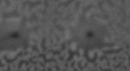
1 Simple method for formation of nanometer scale holes in membranes T. Schenkel 1, E. A. Stach, V. Radmilovic, S.-J. Park, and A. Persaud E. O. Lawrence Berkeley National Laboratory, Berkeley, CA When nanometer scale holes (diameters of 50 to a few hundred nm) are imaged in a scanning electron microscope (SEM) at pressures in the 10-5 to 10-6 torr range, hydrocarbon deposits built up and result in the closing of holes within minutes of imaging. Additionally, electron beam deposition of material from a gas source allows the closing of holes with films of platinum or TEOS oxide. In an instrument equipped both with a focused ion beam (FIB), and an SEM, holes can be formed and then covered with a thin film to form nanopores with controlled openings, ranging down to only a few nanometers. The ability to form holes in membranes with diameters of only a few nanometers (1 to 10 nm) is of interest in many fields of nanometer scale science including single molecule studies, ion proximity lithography, and single atom doping [1-5]. Electron beam lithography followed by dry etching has been used to form holes with diameters in the range of tens of nanometers, but resist resolution and etching of high aspect ratio holes in membranes make formation of holes with diameters below 5 nm very challenging [6]. Direct hole drilling can be achieved with focused ion beams, but available beam diameters are about 10 nm, limiting achievable hole sizes. Holes can also be drilled directly with electron beams, and hole diameters as small as 1 to 2 nm have been reported in 100 nm thick sheets of Al 2 O 3 [7]. Formation of synthetic nanometer 1 T_Schenkel@LBL.gov 1
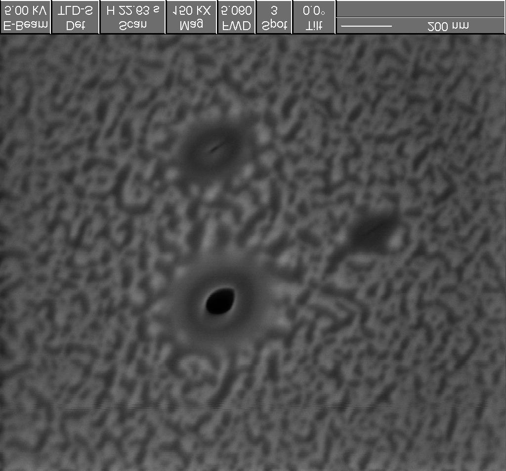
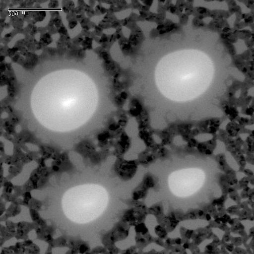
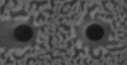
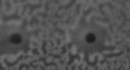
2 scale holes with diameters below 10 nm has further been reported by several groups who used swift heavy ion track etching [3], or ion beam sculpting with kev argon ions [1, 8]. In this letter, we describe a simple method for nano-hole formation based on monitored closing of 100 nm scale holes by electron beam deposition of thin films. For our experiments at the National Center for Electron Microscopy at LBNL we used an FEI dual beam FIB, a system combining a focused ion beam with an SEM column. Samples in our study were membranes of low stress silicon nitride with a thickness of 200 nm on silicon frames. Membranes were coated with 5 nm of a gold palladium alloy to prevent charging during exposure to charged particle beams. A 30 kev Ga + beam with an intensity of 1 pa in spot with a diameter of 10 nm was used to drill holes into the membranes. Initial hole diameters ranged from about 50 to 200 nm. The base pressure in the FIB vacuum chamber was torr. For hole closing with hydro-carbon films (also known as contamination resist [9]), an electron beam (5 kev, 1 na, nominal spot size 2 nm) was rastered over the area with the initial hole pattern at a magnification of 150,000 to 350,000 at a rate of 5 scans per second. After an exposure interval of 30 s to one minute, the sample area was imaged with a slower, higher contrast scan, and the process was repeated. In Figure 1, we show a sequence of images of three holes taken immediately following FIB drilling (a) and after several minutes of electron beam exposure (b and c). Under these conditions, the rate of hole closing was linear with a slope of 0.3 nm/s (Figure 2). The chemical composition of the deposited material can be elucidated through a comparision of SEM and ransmission electron microscope images of closed holes. In Figure 3, we show a pattern of closed holes in SEM (a) and TEM (b) images. In SEM, contrast was obtained by detection of backscattered electrons, 2
3 the yield of which is proportional to the square of the atomic number of imaged materials (~Z 2 ) In SEM images, the Au/Pd islands appear bright, while the silicon nitride substrate and the material that covers the holes appear dark. In TEM, contrast is based on absorption and scattering of electrons by atoms in the films, and contrast is reversed compared to SEM with backscattered electrons. The high Z Au/Pd film appears dark, while the silicon nitride is lighter and the material that closed the holes is very light. TEM contrast is a convolution of film composition and film thickness. Comparison of SEM and TEM images makes the conclusion plausible that the holes close due to built-up of a low Z hydrocarbon layer during electron beam exposure. The possibility of formation of a film from the Au/Pd layer can be excluded. TEM images also confirm that the holes have not been closed completely. Rather the original hole diameter was reduced to about 5 nm, well below the resolution of direct FIB drilling. Holes can also be closed by electron beam deposition of selected materials, like TEOS oxide and many metals. Here, the to be deposited material is introduced into the vacuum chamber through a gas needle that exposes an area of interest to the selected compound. We have tested this for platinum deposition. The platinum containing gas was admitted into the chamber for pulses of few seconds during which the electron beam rastered over the region of interest. As expected, the holes closed during deposition of the platinum film. In the examples shown in Figure 4, the diameters of two holes were reduced from 175 nm to 30 nm by electron beam deposition of platinum. The hole diameters were reduced at an average rate of 10 nm/s, over thirty times faster then for deposition of hydro-carbon films. The hole closing rate was found to slow down to a rate of 6 nm/s after 10 s, an effect that is currently under closer investigation. Reduction of 3
4 hole diameters from 225 nm to 40 nm by thin film deposition with magnetron sputtering was reported by Ruchhoeft et al. [4]. In these studies, apertures closed at a rate of 0.64 nm per nm of deposited Au. The advantage of the local electron beam deposition described here is that hole evolution is monitored directly, so that the formation of very small holes becomes possible. Control of gas flux and local pressure are important for the reproducible formation of holes with desired sizes, and with minimal contamination of the area exposed to the seed gas. Hole closing rates, and film thicknesses for a given hole size for hydrocarbon or metal deposition depend on many parameters, such as electron beam current, scan rate, residual vacuum composition, and systematic studies of hole closing by electron beam deposition are underway. In situ electron beam or ion beam deposition of metal nanowires enables integration of nano-holes with electrodes for switching and monitoring of selected holes. The results shown here demonstrate a simple method for the formation of nanometer scale holes by electron beam deposition of thin films. Holes, formed by FIB drilling or other methods, can be closed while their structure is being monitored. Electron beam deposition of thin films allows the formation of holes in a wide variety of materials (contamination resist, metals and TEOS oxide). Hole evolution can be monitored in situ down to the resolution limits of the available SEM (typically 2 to 5 nm). Hole diameters of about 2 nm are important for single molecule studies, potential applications in DNA sequencing [1-3], and ultrahigh resolution single atom doping [5]. Scaling of hole closing rates under controlled conditions allows formation of holes with diameters at and even below the SEM resolution limit. The presented simple method represent a hybrid of top down and bottom up techniques and enables structure formation 4
5 beyond primary beam size limits though a primitive form of self organization during thin film deposition. Acknowledgments T. S. acknowledges stimulating discussions with A. Schmid, I. Rangelow, and J. A. Liddle. This work was supported by the National Security Agency (NSA) and Advanced Research and Development Activity (ARDA) under Army Research Office (ARO) contract number MOD707501, and by the U. S. Department of Energy under Contract No. DE-AC03-76SF References [1] J. Li, D. Stein, C. McMullan, D. Branton, M. J. Azis, and J. A. Golovchenko, Nature 412, 166 (2001) [2] A. Meller, L. Nivon, and D. Branton, Phys. Rev. Lett. 86, 3435 (2001) [3] Z. Siwy and A. Fuliski, Phys. Rev. Lett. 89, (2002) [4] P. Ruchhoeft, et al., J. Vac. Sci. Technol. B 20, 2705 (2002) [5] T. Schenkel, et al., J. Vac. Sci. Technol. 20, 2819 (2002) [6] A. N. Broers, A. C. F. Hoole, J. M. Ryan, Microel. Engin. 32, 131 (1996) [7] M. E. Mochel, et al., Apl. Phys. Lett. 44, 502 (1984) [8] D. Stein, J. Li, and J. A. Golovchenko, Phys. Rev. Lett. 89, (2002) [9] W. W. Molzen, et al., J. Vac. Sci. Technol. 16, 269 (1979); C. P. Umbach, et al., J. Vac. Sci. Technol. B 4, 383 (1986) 5
 close after minutes of exposure to the 5 kev electron beam (middle, bottom). The surface structure surrounding the holes is from the thin Au/Pd film.")
6 Figure captions: Figure 1: SEM images of three FIB drilled holes in a 200 nm thick silicon nitride membrane. The original holes (top) close after minutes of exposure to the 5 kev electron beam (middle, bottom). The surface structure surrounding the holes is from the thin Au/Pd film. Figure 2: Hole diameters as a function of time of electron beam exposure. The line is a linear fit to one data set and shows a closing rate of 0.3 nm/s. Figure 3: SEM (left) and TEM (right) images of holes after closing by electron beam exposure. Contrast in the SEM is from backscattered electrons, which yields Z contrast. The high Z Au/Pd film appears bright, while the silicon nitride and the hole closing film appear darker. In TEM, contrast is reversed, and the hole closing film appears bright, indicating hole closing with low Z hydro-carbons. Figure 4: Two FIB drilled holes (top) are closed by platinum deposition from an organometallic vapor during electron beam exposure (middle, bottom). 6

7 Figure 1 7
8 hole diameter (nm) fib-closing-1b 3 SEM imaging time (s) Figure 2 8

9 Figure 3 9
10 Fig. 4 10
In-Situ Nanoindentation of Epitaxial TiN/MgO (001) in a Transmission Electron Microscope
 in a Transmission Electron Microscope") Journal of ELECTRONIC MATERIALS, Vol. 32, No. 10, 2003 Special Issue Paper In-Situ Nanoindentation of Epitaxial TiN/MgO (001) in a Transmission Electron Microscope A.M. MINOR, 1,5 E.A. STACH, 2 J.W. MORRIS,
Journal of ELECTRONIC MATERIALS, Vol. 32, No. 10, 2003 Special Issue Paper In-Situ Nanoindentation of Epitaxial TiN/MgO (001) in a Transmission Electron Microscope A.M. MINOR, 1,5 E.A. STACH, 2 J.W. MORRIS,
Nanoscale Imaging, Material Removal and Deposition for Fabrication of Cutting-edge Semiconductor Devices
 Hitachi Review Vol. 65 (2016), No. 7 233 Featured Articles Nanoscale Imaging, Material Removal and Deposition for Fabrication of Cutting-edge Semiconductor Devices Ion-beam-based Photomask Defect Repair
In-situ monitoring of optical near-field material processing by electron microscopes
 Appl Phys A DOI 10.1007/s00339-011-6615-6 INVITED PAPER In-situ monitoring of optical near-field material processing by electron microscopes David J. Hwang Bin Xiang Sang-Gil Ryu Oscar Dubon Andrew M.
Transmission Kikuchi Diffraction in the Scanning Electron Microscope
 Transmission Kikuchi Diffraction in the Scanning Electron Microscope Robert Keller, Roy Geiss, Katherine Rice National Institute of Standards and Technology Nanoscale Reliability Group Boulder, Colorado
IBS/e Ion Beam Sputter Deposition and Etching System. IBS/e with KDC-10 Ion Beam Sputter Deposition and Etching System with Kaufman Ion Source
 IBS/e Ion Beam Sputter Deposition and Etching System IBS/e with KDC-10 Ion Beam Sputter Deposition and Etching System with Kaufman Ion Source The Model IBS/e is a high vacuum thin film deposition system
Specimen Preparation Technique for a Microstructure Analysis Using the Focused Ion Beam Process
 Specimen Preparation Technique for a Microstructure Analysis Using the Focused Ion Beam Process by Kozue Yabusaki * and Hirokazu Sasaki * In recent years the FIB technique has been widely used for specimen
EECS130 Integrated Circuit Devices
 EECS130 Integrated Circuit Devices Professor Ali Javey 9/13/2007 Fabrication Technology Lecture 1 Silicon Device Fabrication Technology Over 10 15 transistors (or 100,000 for every person in the world)
Scanning Electron Microscope & Surface Analysis. Wageningen EM Centre Marcel Giesbers
 Scanning Electron Microscope & Surface Analysis Wageningen EM Centre Marcel Giesbers Scanning Electron Microscope & Surface Analysis SEM vs Light Microscope and Transmission EM Secondary Electron Imaging
Metallization deposition and etching. Material mainly taken from Campbell, UCCS
 Metallization deposition and etching Material mainly taken from Campbell, UCCS Application Metallization is back-end processing Metals used are aluminum and copper Mainly involves deposition and etching,
High Performance Lithium Battery Anodes Using Silicon Nanowires
 Supporting Online Materials For High Performance Lithium Battery Anodes Using Silicon Nanowires Candace K. Chan, Hailin Peng, Gao Liu, Kevin McIlwrath, Xiao Feng Zhang, Robert A. Huggins and Yi Cui * *To
Differentially pumped quadrupole SIMS probe on FIBbased and two-beam microscopes
 Differentially pumped quadrupole SIMS probe on FIBbased and two-beam microscopes Richard J Chater (1), Barbara Shollock (1), David McPhail (1), Alan J Smith (2) and Graham Cooke (2) (1) Department of Materials,
Scanning thermal microscopy probe capable of simultaneous electrical imaging and the addition of a diamond tip
 Scanning thermal microscopy probe capable of simultaneous electrical imaging and the addition of a diamond tip E Brown, L Hao, D C Cox and J C Gallop National Physical Laboratory, Hampton Road, Teddington,
Product Information Version 2.0. ZEISS ORION NanoFab Three Ion Beams for Enhanced Flexibility in Sub-10 nm Fabrication
 Product Information Version 2.0 ZEISS ORION NanoFab Three Ion Beams for Enhanced Flexibility in Sub-10 nm Fabrication Three Ion Beams for Enhanced Flexibility in Sub-10 nm Fabrication Fabricate sub-10
Specimen configuration
 APPLICATIONNOTE Model 1040 NanoMill TEM specimen preparation system Specimen configuration Preparing focused ion beam (FIB) milled specimens for submission to Fischione Instruments. The Model 1040 NanoMill
Physical Vapor Deposition (PVD) Zheng Yang
 Zheng Yang") Physical Vapor Deposition (PVD) Zheng Yang ERF 3017, email: yangzhen@uic.edu Page 1 Major Fabrication Steps in MOS Process Flow UV light Mask oxygen Silicon dioxide photoresist exposed photoresist oxide
Physical Vapor Deposition (PVD) Zheng Yang ERF 3017, email: yangzhen@uic.edu Page 1 Major Fabrication Steps in MOS Process Flow UV light Mask oxygen Silicon dioxide photoresist exposed photoresist oxide
Platypus Gold Coated Substrates. Bringing Science to the Surface
 Platypus Gold Coated Substrates Bringing Science to the Surface Overview Gold Coated Substrates - Gold Coating Introduction - Glossary of Terms - Gold Coating Methods - Critical Features Platypus Gold
MODEL PicoMill TEM specimen preparation system. Achieve ultimate specimen quality free from amorphous and implanted layers
 MODEL 1080 PicoMill TEM specimen preparation system Combines an ultra-low energy, inert gas ion source, and a scanning electron column with multiple detectors to yield optimal TEM specimens. POST-FIB PROCESSING
Mini RF-driven ion sources for focused ion beam systems
 Mini RF-driven ion sources for focused ion beam systems X. Jiang a), Q. Ji, A. Chang, and K. N. Leung. Lawrence Berkeley National Laboratory, University of California, Berkeley, California 94720 Abstract
Improvement of gas barrier properties by combination of polymer film and gas barrier layer
 Improvement of gas barrier properties by combination of polymer film and gas barrier Y. Tsumagari, H. Murakami, K. Iseki and S. Yokoyama Toyobo Co., LTD. RESEARCH CENTER, - Katata 2-chome, Otsu, Shiga,
Cross sectional TEM analysis of duplex HIPIMS and DC magnetron sputtered Mo and W doped carbon coatings
 Cross sectional TEM analysis of duplex HIPIMS and DC magnetron sputtered Mo and W doped carbon coatings SHARP, J, MULLER, I Castillo, MANDAL, P, ABBAS, A, WEST, G, RAINFORTH, W M, EHIASARIAN, Arutiun
Electrical Characterization of Tungsten Nanowires Deposited by Focused Ion Beam (FIB) *
 *") Nanopages 1 (2006) 2, 255 262 DOI: 10.1556/Nano.1.2006.2.10 Electrical Characterization of Tungsten Nanowires Deposited by Focused Ion Beam (FIB) * E. Horváth 1,2**, P. L. Neumann 2, A. L. Tóth 1, É. Vázsonyi
Nanopages 1 (2006) 2, 255 262 DOI: 10.1556/Nano.1.2006.2.10 Electrical Characterization of Tungsten Nanowires Deposited by Focused Ion Beam (FIB) * E. Horváth 1,2**, P. L. Neumann 2, A. L. Tóth 1, É. Vázsonyi
Cross sectional TEM analysis of duplex HIPIMS and DC magnetron sputtered Mo and W doped carbon coatings
 Cross sectional TEM analysis of duplex HIPIMS and DC magnetron sputtered Mo and W doped carbon coatings SHARP, J, MULLER, I Castillo, MANDAL, P, ABBAS, A, WEST, G, RAINFORTH, W M, EHIASARIAN, Arutiun and
HIGH SPATIAL RESOLUTION AND HIGH ENERGY RESOLUTION AUGER DEPTH PROFILING
 Application Note HIGH SPATIAL RESOLUTION AND HIGH ENERGY RESOLUTION AUGER DEPTH PROFILING of / Films OVERVIEW The formation processes of nickel silicide thin films are of particular interest for sub-65
Micro-Nano Fabrication Research
 Micro-Nano Fabrication Research Technical Education Quality Improvement Programme 22-23 December 2014 Dr. Rakesh G. Mote Assistant Professor Department of Mechanical Engineering IIT Bombay rakesh.mote@iitb.ac.in;
Previous Lecture. Vacuum & Plasma systems for. Dry etching
 Previous Lecture Vacuum & Plasma systems for Dry etching Lecture 9: Evaporation & sputtering Objectives From this evaporation lecture you will learn: Evaporator system layout & parts Vapor pressure Crucible
Thin Films: Sputtering Systems (Jaeger Ch 6 & Ruska Ch 7,) Can deposit any material on any substrate (in principal) Start with pumping down to high
 Can deposit any material on any substrate (in principal) Start with pumping down to high") Thin Films: Sputtering Systems (Jaeger Ch 6 & Ruska Ch 7,) Can deposit any material on any substrate (in principal) Start with pumping down to high vacuum ~10-7 torr Removes residual gases eg oxygen from
Thin Films: Sputtering Systems (Jaeger Ch 6 & Ruska Ch 7,) Can deposit any material on any substrate (in principal) Start with pumping down to high vacuum ~10-7 torr Removes residual gases eg oxygen from
Visualization and Control of Particulate Contamination Phenomena in a Plasma Enhanced CVD Reactor
 Visualization and Control of Particulate Contamination Phenomena in a Plasma Enhanced CVD Reactor Manabu Shimada, 1 Kikuo Okuyama, 1 Yutaka Hayashi, 1 Heru Setyawan, 2 and Nobuki Kashihara 2 1 Department
Vertically aligned Ni magnetic nanowires fabricated by diblock-copolymer-directed Al thin film anodization
 Vertically aligned Ni magnetic nanowires fabricated by diblock-copolymer-directed Al thin film anodization Researcher: Kunbae (Kevin) Noh, Graduate Student, MAE Dept. and CMRR Collaborators: Leon Chen,
THIN METALLIC LAYERS STRUCTURED BY E-BEAM LITHOGRAPHY. Miroslav HORÁČEK, Vladimír KOLAŘÍK, Michal URBÁNEK, František MATĚJKA, Milan MATĚJKA
 THIN METALLIC LAYERS STRUCTURED BY E-BEAM LITHOGRAPHY Miroslav HORÁČEK, Vladimír KOLAŘÍK, Michal URBÁNEK, František MATĚJKA, Milan MATĚJKA Ústav přístrojové techniky AV ČR, v. v. i., Královopolská 147,
Sputter Coating. Technical Brief
 Sputter Coating Technical Brief Document Number TB-SPUTTER Issue 2 (01/02) Introduction HP000107 Quorum Technologies Ltd main sales office: South Stour Avenue Ashford Kent U.K. Tel: ++44(0) 1233 646332
PARAMETER EFFECTS FOR THE GROWTH OF THIN POROUS ANODIC ALUMINUM OXIDES
 10.1149/1.2794473, The Electrochemical Society PARAMETER EFFECTS FOR THE GROWTH OF THIN POROUS ANODIC ALUMINUM OXIDES S. Yim a, C. Bonhôte b, J. Lille b, and T. Wu b a Dept. of Chem. and Mat. Engr., San
SOLID SOLUTION METAL ALLOYS
 SOLID SOLUTION METAL ALLOYS Synergy Effects vs. Segregation Phenomena D. Manova, J. Lutz, S. Mändl, H. Neumann 1 Table of Content Motivation Alloys vs. Pure Elements or Intermetallic Compounds Introduction
Introduction to Lithography
 Introduction to Lithography G. D. Hutcheson, et al., Scientific American, 290, 76 (2004). Moore s Law Intel Co-Founder Gordon E. Moore Cramming More Components Onto Integrated Circuits Author: Gordon E.
Supporting Information for Effects of Thickness on the Metal-Insulator Transition in Free-Standing Vanadium Dioxide Nanocrystals
 Supporting Information for Effects of Thickness on the Metal-Insulator Transition in Free-Standing Vanadium Dioxide Nanocrystals Mustafa M. Fadlelmula 1,2, Engin C. Sürmeli 1,2, Mehdi Ramezani 1,2, T.
XTEM characterization of modulated ion implantation through self-organized anodic aluminium oxide (AAO) membranes
 membranes") XTEM characterization of modulated ion implantation through self-organized anodic aluminium oxide (AAO) membranes Wei Guan 1, Jay Ghatak 1, Nianhua Peng 2, Yong Peng 1, Chris Jeynes 2, Beverley Inkson
XTEM characterization of modulated ion implantation through self-organized anodic aluminium oxide (AAO) membranes Wei Guan 1, Jay Ghatak 1, Nianhua Peng 2, Yong Peng 1, Chris Jeynes 2, Beverley Inkson
JSM-7800F Field Emission Scanning Electron Microscope
 JSM-7800F catalogue JSM-7800F Field Emission Scanning Electron Microscope We provide high performance The Ultimate Research Tool for Multi-Disciplinary Research Institutions Extreme resolution The super
Supporting Online Materials
 Supporting Online Materials Electron Microscopy Observation of TiO 2 Nanocrystal Evolution in High- Temperature Atomic Layer Deposition Jian Shi, 1, Zhaodong Li, 1 Alexander Kvit, 1,2 Sergiy Krylyuk, 3
Gas field ion source and liquid metal ion source charged particle material interaction study for semiconductor nanomachining applications
 Gas field ion source and liquid metal ion source charged particle material interaction study for semiconductor nanomachining applications Shida Tan, a Richard Livengood, and Darryl Shima Intel Corporation,
Deposition of niobium and other superconducting materials with high power impulse magnetron sputtering: Concept and first results
 15th International Conference on RF Superconductivity July 25-29, 2011, Chicago Deposition of niobium and other superconducting materials with high power impulse magnetron sputtering: Concept and first
A STUDY OF THE EFFECTIVENESS OF THE REMOVAL OF HYDROCARBON CONTAMINATION BY OXIDATIVE CLEANING INSIDE THE SEM.
 A STUDY OF THE EFFECTIVENESS OF THE REMOVAL OF HYDROCARBON CONTAMINATION BY OXIDATIVE CLEANING INSIDE THE SEM. Neal Sullivan, Tung Mai, Scott Bowdoin* and Ronald Vane** A poster paper presented at Microscopy
Amorphous and Polycrystalline Thin-Film Transistors
 Part I Amorphous and Polycrystalline Thin-Film Transistors HYBRID AMORPHOUS AND POLYCRYSTALLINE SILICON DEVICES FOR LARGE-AREA ELECTRONICS P. Mei, J. B. Boyce, D. K. Fork, G. Anderson, J. Ho, J. Lu, Xerox
Ag 2 S: Fabrication and Characterization Techniques
 2 2 S: Fabrication and Characterization Techniques This chapter describes two fabrication methods used for the growth of 2 S thin films. The specific growth parameters are presented for each method as
Cleaning samples. Options available. » Do not use organic. » Never, never, use squeeze. » Use detergents instead e.g. » Carbon Dioxide snow
 Sample Preparation Cleaning samples» Do not use organic solvents as these are always contaminated, even when fresh electronic grade» Never, never, use squeeze or spray bottles» Use detergents instead e.g.
Supplementary Information
 Supplementary Information Direct manufacturing of ultrathin graphite on three- dimensional nanoscale features Mercè Pacios, Peiman Hosseini, Ye Fan, Zhengyu He, Oliver Krause, John Hutchison, Jamie H.
Fabrication of Highly Ordered Gold Nanorods Film Using Alumina Nanopores
 JNS 2 (2012) 235-240 Fabrication of Highly Ordered Gold Nanorods Film Using Alumina Nanopores Z. Soltani a,*, M. Moradi b, M. Noormohammadi b, F. Behzadi b a Department of Physics, Shiraz Branch, Islamic
Synthesis of Nanostructures by Electrochemical Processing
 Synthesis of Nanostructures by Electrochemical Processing Giovanni Zangari, Robert M. Metzger, Bill Butler University of Alabama at Tuscaloosa The work presented was partly sponsored through DOD grant
Title: Localized surface plasmon resonance of metal nanodot and nanowire arrays studied by far-field and near-field optical microscopy
 Contract Number: AOARD-06-4074 Principal Investigator: Heh-Nan Lin Address: Department of Materials Science and Engineering, National Tsing Hua University, 101, Sec. 2, Kuang Fu Rd., Hsinchu 30013, Taiwan
Growth of monocrystalline In 2 O 3 nanowires by seed orientation dependent vapour-solid-solid mechanism
 Electronic Supplementary Material (ESI) for Journal of Materials Chemistry C. This journal is The Royal Society of Chemistry 2014 Electronic Supplementary Information (ESI) Growth of monocrystalline In
Chapter 3 Silicon Device Fabrication Technology
 Chapter 3 Silicon Device Fabrication Technology Over 10 15 transistors (or 100,000 for every person in the world) are manufactured every year. VLSI (Very Large Scale Integration) ULSI (Ultra Large Scale
A Functional Micro-Solid Oxide Fuel Cell with. Nanometer Freestanding Electrolyte
 Electronic Supplementary Material (ESI) for Journal of Materials Chemistry A. This journal is The Royal Society of Chemistry 2017 SUPPLEMENTARY INFORMATION A Functional Micro-Solid Oxide Fuel Cell with
of Au Nanodots on Ultrathin in-situ Grown Silicon Oxide.
 Variation of Threshold Field in Field Induced Fabrication of Au Nanodots on Ultrathin in-situ Grown Silicon Oxide. Jeong Young Park 1,3, a), R. J. Phaneuf 2,3, and E. D. Williams 1,3 1 Department of Physics,
SUPPLEMENTARY INFORMATIONS
 SUPPLEMENTARY INFORMATIONS Dynamic Evolution of Conducting Nanofilament in Resistive Switching Memories Jui-Yuan Chen, Cheng-Lun Hsin,,, Chun-Wei Huang, Chung-Hua Chiu, Yu-Ting Huang, Su-Jien Lin, Wen-Wei
SEM (SCANNING ELECTRON MICROSCOPE)
") SEM (SCANNING ELECTRON MICROSCOPE) 20823856 Özgen Buğdaycı 20824336 Elif Topçuoğlu 20823985 Yavuz Duran Hacettepe University 12.04.2012 OUTLINE Definiton of scanning electron microscope History Usage Area
SEM (SCANNING ELECTRON MICROSCOPE) 20823856 Özgen Buğdaycı 20824336 Elif Topçuoğlu 20823985 Yavuz Duran Hacettepe University 12.04.2012 OUTLINE Definiton of scanning electron microscope History Usage Area
Advanced Manufacturing Choices
 Advanced Manufacturing Choices Table of Content Mechanical Removing Techniques Ultrasonic Machining (USM) Sputtering and Focused Ion Beam Milling (FIB) Ultrasonic Machining In ultrasonic machining (USM),
Study of Ion Beam Sputtering using Different Materials
 ab Journal of Nuclear Science and Applications, 5(), Study of Ion Beam Sputtering using Different Materials H. El-Khabeary Accelerators & Ion Sources Department, Basic Nuclear Science Division, Nuclear
The Hummer VI. Brian Thomas Lithography. October 29, Hummer VI THE UNIVERSITY OF TEXAS AT DALLAS ERIK JOHNSON SCHOOL OF ENGINEERING
 The Hummer VI Brian Thomas Lithography October 29, 2003 Hummer VI THE UNIVERSITY OF TEXAS AT DALLAS ERIK JOHNSON SCHOOL OF ENGINEERING DOCUMENT NUMBER: FA2003-LI-006 EDITION: 1.0 PAGE: 1 of 6 The Hummer
Novel Fuel Cell MEA Based on Pt-C Deposited by Magnetron Sputtering
 10.1149/08008.0225ecst The Electrochemical Society Novel Fuel Cell MEA Based on Pt-C Deposited by Magnetron Sputtering A. Ostroverkh a, V. Johanek a, M. Dubau a, P. Kus a, K. Veltruska a, M. Vaclavu a,
Linear Plasma Sources for Surface Modification and Deposition for Large Area Coating
 Linear Plasma Sources for Surface Modification and Deposition for Large Area Coating Dr Tony Williams Gencoa Ltd, UK Victor Bellido-Gonzalez, Dr Dermot Monaghan, Dr Joseph Brindley, Robert Brown SVC 2016,
Ultra-high material-quality silicon pillars on glass. IEEE Photovoltaic Specialists Conference Conference Record. Copyright IEEE.
 Title Ultra-high material-quality silicon pillars on glass Author(s) Liu, F; AI-Jassim, MM; Young, DL Citation The 35th IEEE Photovoltaic Specialists Conference (PVSC 2010), Honolulu, HI., 20-25 June 2010.
Ballistic current transport studies of ferromagnetic multilayer films and tunnel junctions invited
 JOURNAL OF APPLIED PHYSICS VOLUME 89, NUMBER 11 1 JUNE 2001 Growth of Magnetic Tunnel Junctions Jeff Childress, Chairman Ballistic current transport studies of ferromagnetic multilayer films and tunnel
Materials Synthesis Via Directed Vapor Deposition
 Chapter 6 Materials Synthesis Via Directed Vapor Deposition 6.1 Overview Experimental work was undertaken to explore the ability of Directed Vapor Deposition to synthesize a variety of films in a low vacuum
Combinatorial RF Magnetron Sputtering for Rapid Materials Discovery: Methodology and Applications
 Combinatorial RF Magnetron Sputtering for Rapid Materials Discovery: Methodology and Applications Philip D. Rack,, Jason D. Fowlkes, and Yuepeng Deng Department of Materials Science and Engineering University
Fabrication Process. Crystal Growth Doping Deposition Patterning Lithography Oxidation Ion Implementation CONCORDIA VLSI DESIGN LAB
 Fabrication Process Crystal Growth Doping Deposition Patterning Lithography Oxidation Ion Implementation 1 Fabrication- CMOS Process Starting Material Preparation 1. Produce Metallurgical Grade Silicon
Universität Hamburg, Hamburg, Germany. Universität Hamburg, Hamburg, Germany
 Sample Preparation, Micromagnetic Simulations, Circular-Rotational Currents, Parasitic Oersted Fields and Clover Samples (Magnetic Antivortex-Core Reversal by Circular-Rotational Spin Currents) Thomas
Influence of Alloy Microstructure on Oxide Growth in HCM12A in Supercritical Water
 Mater. Res. Soc. Symp. Proc. Vol. 1125 2009 Materials Research Society 1125-R06-05 Influence of Alloy Microstructure on Oxide Growth in HCM12A in Supercritical Water Jeremy Bischoff 1, Arthur T. Motta
Grain Contrast Imaging in UHV SLEEM
 Materials Transactions, Vol. 51, No. 2 (2010) pp. 292 to 296 Special Issue on Development and Fabrication of Advanced Materials Assisted by Nanotechnology and Microanalysis #2010 The Japan Institute of
Controllable growth of aluminum nanorods using physical vapor deposition
 Stagon and Huang Nanoscale Research Letters 2014, 9:400 NANO EXPRESS Open Access Controllable growth of aluminum nanorods using physical vapor deposition Stephen P Stagon 1,2 and Hanchen Huang 1* Abstract
Heteroepitaxy of Monolayer MoS 2 and WS 2
 Supporting Information Seed Crystal Homogeneity Controls Lateral and Vertical Heteroepitaxy of Monolayer MoS 2 and WS 2 Youngdong Yoo, Zachary P. Degregorio, James E. Johns* Department of Chemistry, University
In-situ laser-induced contamination monitoring using long-distance microscopy
 In-situ laser-induced contamination monitoring using long-distance microscopy Paul Wagner a, Helmut Schröder* a, Wolfgang Riede a a German Aerospace Center (DLR), Institute of Technical Physics, Pfaffenwaldring
Manufacturability of highly doped Aluminum Nitride films
 Manufacturability of highly doped Aluminum Nitride films Sergey Mishin Yury Oshmyansky Advanced Modular Systems, Inc Goleta, CA/USA smishin@amssb.com yoshmyansky@amssb.com Abstract There have been several
Electron Beam Lithography - key enabling technology in nanofabrication. Frank Dirne
 Electron Beam Lithography - key enabling technology in nanofabrication Frank Dirne Moore s Law (x2/2 yr) Moore s Law EBL Electron Beam Lithography - key enabling technology in nanofabrication - Principles
Evolution of atomic-scale roughening on Si(001)-(2 1) surfaces resulting from high temperature oxidation
-(2 1) surfaces resulting from high temperature oxidation") Evolution of atomic-scale roughening on Si(001)-(2 1) surfaces resulting from high temperature oxidation J. V. Seiple and J. P. Pelz Department of Physics, The Ohio State University, Columbus, Ohio 43210
Evolution of atomic-scale roughening on Si(001)-(2 1) surfaces resulting from high temperature oxidation J. V. Seiple and J. P. Pelz Department of Physics, The Ohio State University, Columbus, Ohio 43210
Electrical properties of thin rf sputtered aluminum oxide films
 Materials Science and Engineering B 109 (2004) 99 103 Electrical properties of thin rf sputtered aluminum oxide films M. Voigt, M. Sokolowski Institut für Physikalische und Theoretische Chemie der Universität
Morphology of Thin Aluminum Film Grown by DC Magnetron Sputtering onto SiO 2 on Si(100) Substrate
 Substrate") Morphology of Thin Aluminum Film Grown by DC Magnetron Sputtering onto SiO 2 on Si(1) Substrate Fan Wu Microelectronics Center, Medtronic Inc., Tempe, AZ 85261 James E. Morris Department of Electrical
Morphology of Thin Aluminum Film Grown by DC Magnetron Sputtering onto SiO 2 on Si(1) Substrate Fan Wu Microelectronics Center, Medtronic Inc., Tempe, AZ 85261 James E. Morris Department of Electrical
EFFECT OF GROWTH TEMPERATURE ON THE CATALYST-FREE GROWTH OF LONG SILICON NANOWIRES USING RADIO FREQUENCY MAGNETRON SPUTTERING
 International Journal of Nanoscience Vol. 10, Nos. 1 & 2 (2011) 13 17 #.c World Scienti c Publishing Company DOI: 10.1142/S0219581X11007594 EFFECT OF GROWTH TEMPERATURE ON THE CATALYST-FREE GROWTH OF LONG
Access to the published version may require subscription. Published with permission from: Institute of Physics
 http://uu.diva-portal.org This is an author produced version of a paper published in Journal of Physics, Conference Series. This paper has been peer-reviewed but does not include the final publisher proof-corrections
Electron Microscopy Sciences Industry Road. P.O. Box 550. Hatfield, PA Introduction. DuraSiNTM
 DuraSiNTM Electron Microscopy Sciences Introduction DuraSiN TM Film and Mesh products have revolutionized the way samples are prepared for and analyzed in the transmission electron microscope. DuraSiN
MODEL SEM Mill. Two independently adjustable TrueFocus ion sources
 MODEL 1060 SEM Mill A state-of-the-art ion milling and polishing system. It is compact, precise, and consistently produces high-quality scanning electron microscopy (SEM) samples for a wide variety of
Metal-containing diamond-like carbon with self-assembled alternating nano-scaled layers
 Metal-containing diamond-like carbon with self-assembled alternating nano-scaled layers Wan-Yu Wu, Jyh-Ming Ting* Mina Materials Laboratory, Department of Materials Science and Engineering, National Cheng
Grain Sizes and Surface Roughness in Platinum and Gold Thin Films. L.L. Melo, A. R. Vaz, M.C. Salvadori, M. Cattani
 Journal of Metastable and Nanocrystalline Materials Vols. 20-21 (2004) pp. 623-628 online at http://www.scientific.net 2004 Trans Tech Publications, Switzerland Grain Sizes and Surface Roughness in Platinum
In-situ Electron Microscopy Mechanical Testing for Steels
 Technical Report UDC 621. 385. 2 : 620. 17 : 669. 14 In-situ Electron Microscopy Mechanical Testing for Steels Shunsuke TANIGUCHI* Gerhard DEHM Abstract This paper outlines the techniques of in-situ electron
PHS6317 NANO-ENGINEERING OF THIN FILMS
 PHS6317 NANO-ENGINEERING OF THIN FILMS Ludvik Martinu, ing., PhD Professor Chairholder: NSERC Multisectorial Industrial Research Chair in Coatings and Surface Engineering ludvik.martinu@polymtl.ca www.polymtl.ca/larfis
Electrical properties of thin rf sputtered aluminum oxide films
 Materials Science and Engineering Bxxx (2004) xxx xxx Electrical properties of thin rf sputtered aluminum oxide films M. Voigt, M. Sokolowski Institut für Physikalische und Theoretische Chemie der Universität
SUPPLEMENTARY INFORMATION
 High Electrochemical Activity of the Oxide Phase in Model Ceria- and Ceria-Ni Composite Anodes William C. Chueh 1,, Yong Hao, WooChul Jung, Sossina M. Haile Materials Science, California Institute of Technology,
Supporting Information: Model Based Design of a Microfluidic. Mixer Driven by Induced Charge Electroosmosis
 Supporting Information: Model Based Design of a Microfluidic Mixer Driven by Induced Charge Electroosmosis Cindy K. Harnett, Yehya M. Senousy, Katherine A. Dunphy-Guzman #, Jeremy Templeton * and Michael
Thin Films: Sputtering Systems (Jaeger Ch 6 & Ruska Ch 7,) Sputtering: gas plasma transfers atoms from target to substrate Can deposit any material
 Sputtering: gas plasma transfers atoms from target to substrate Can deposit any material") Thin Films: Sputtering Systems (Jaeger Ch 6 & Ruska Ch 7,) Sputtering: gas plasma transfers atoms from target to substrate Can deposit any material on any substrate (in principal) Start with pumping down
Thin Films: Sputtering Systems (Jaeger Ch 6 & Ruska Ch 7,) Sputtering: gas plasma transfers atoms from target to substrate Can deposit any material on any substrate (in principal) Start with pumping down
Application Note #124 VITA: Quantitative Nanoscale Characterization and Unambiguous Material Identification for Polymers
 Local thermal analysis identifies polymer AFM image of polymer blend Application Note #124 VITA: Quantitative Nanoscale Characterization and Unambiguous Material Identification for Polymers VITA module
Deposited by Sputtering of Sn and SnO 2
 Journal of the Korean Ceramic Society Vol. 49, No. 5, pp. 448~453, 2012. http://dx.doi.org/10.4191/kcers.2012.49.5.448 Comparative Study of Nitrogen Incorporated SnO 2 Deposited by Sputtering of Sn and
The principles and practice of electron microscopy
 The principles and practice of electron microscopy Second Edition Ian M. Watt CAMBRIDGE UNIVERSITY PRESS Contents Preface tofirstedition page ix Preface to second edition xi 1 Microscopy with light and
TED PELLA, INC. Microscopy Products for Science and Industry
 PELCO SILICON NITRIDE, SILICON DIOXIDE, BLANK SILICON SUBSTRATES & APERTURES FOR TEM Clean, Debris-free with Exact 3mm TEM Frame and EasyGrip Edges PELCO Silicon Nitride Support Films for TEM Hydrophilic
Silver Diffusion Bonding and Layer Transfer of Lithium Niobate to Silicon
 Chapter 5 Silver Diffusion Bonding and Layer Transfer of Lithium Niobate to Silicon 5.1 Introduction In this chapter, we discuss a method of metallic bonding between two deposited silver layers. A diffusion
EUV optics lifetime Radiation damage, contamination, and oxidation
 EUV optics lifetime Radiation damage, contamination, and oxidation M. van Kampen ASML Research 10-11-2016 Preamble Slide 2 ASML builds lithography scanners High-resolution photocopiers Copies mask pattern
The Physical Structure (NMOS)
") The Physical Structure (NMOS) Al SiO2 Field Oxide Gate oxide S n+ Polysilicon Gate Al SiO2 SiO2 D n+ L channel P Substrate Field Oxide contact Metal (S) n+ (G) L W n+ (D) Poly 1 3D Perspective 2 3 Fabrication
The Physical Structure (NMOS) Al SiO2 Field Oxide Gate oxide S n+ Polysilicon Gate Al SiO2 SiO2 D n+ L channel P Substrate Field Oxide contact Metal (S) n+ (G) L W n+ (D) Poly 1 3D Perspective 2 3 Fabrication
Effect of Oxidation Protection Layer on the Performance of Magnetic Force Microscope Tip
 Effect of Oxidation Protection Layer on the Performance of Magnetic Force Microscope Tip Keiichi Kato, Mitsuru Ohtake, Masaaki Futamoto, Fumiyoshi Kirino *, and Nobuyuki Inaba ** Faculty of Science and
Introduction. 1. Sputtering process, target materials and their applications
 Sputtering is widely used in the production of electronic devices such as liquid crystal displays (LCDs), optical media, magnetic media and semiconductors. The Kobelco Research Institute, Inc. has been
Author(s) Chayahara, A; Kinomura, A; Horino, RightCopyright 1999 American Vacuum Soci
 Chayahara, A; Kinomura, A; Horino, RightCopyright 1999 American Vacuum Soci") Title Titanium nitride prepared by plasma implantation Author(s) Yukimura, K; Sano, M; Maruyama, T; Chayahara, A; Kinomura, A; Horino, Citation JOURNAL OF VACUUM SCIENCE & (1999), 17(2): 840-844 TECHNOL
Title Titanium nitride prepared by plasma implantation Author(s) Yukimura, K; Sano, M; Maruyama, T; Chayahara, A; Kinomura, A; Horino, Citation JOURNAL OF VACUUM SCIENCE & (1999), 17(2): 840-844 TECHNOL
Hydrogen-induced surface blistering of sample chuck materials in hydrogen plasma immersion ion implantation
 Hydrogen-induced surface blistering of sample chuck materials in hydrogen plasma immersion ion implantation Paul K. Chu a) and Xuchu Zeng Department of Physics and Materials Science, City University of
Grids for Applications in High-Temperature High- Resolution Transmission Electron Microscopy
 Grids for Applications in High-Temperature High- Resolution Transmission Electron Microscopy The MIT Faculty has made this article openly available. Please share how this access benefits you. Your story
Grids for Applications in High-Temperature High- Resolution Transmission Electron Microscopy
 Grids for Applications in High-Temperature High- Resolution Transmission Electron Microscopy The MIT Faculty has made this article openly available. Please share how this access benefits you. Your story
Aluminium and silicon determination on two Si±Al sputter targets used for magnetron sputtering
 Nuclear Instruments and Methods in Physics Research B 158 (1999) 683±688 www.elsevier.nl/locate/nimb Aluminium and silicon determination on two Si±Al sputter targets used for magnetron sputtering G. Terwagne