Fabrication Technology
|
|
|
- Eleanor Brooks
- 6 years ago
- Views:
Transcription
1 Fabrication Technology By B.G.Balagangadhar Department of Electronics and Communication Ghousia College of Engineering, Ramanagaram 1
2 OUTLINE Introduction Why Silicon The purity of Silicon Czochralski growing process Fabrication processes Thermal Oxidation Etching techniques Diffusion 2
3 Expressions for diffusion of dopant, concentration Ion implantation Photomask generation Photolithography Epitaxial growth Metallization and interconnections, Ohmic contacts Planar PN junction diode fabrication, Fabrication of resistors and capacitors in IC's. 3
4 INTRODUCTION The microminiaturization of electronics circuits and systems and then concomitant application to computers and communications represent major innovations of the twentieth century. These have led to the introduction of new applications that were not possible with discrete devices. Integrated circuits on a single silicon wafer followed by the increase of the size of the wafer to accommodate many more such circuits served to significantly reduce the costs while increasing the reliability of these circuits. 4
5 5
6 WHY SILICON? Semiconductor devices are of two forms (i) Discrete Units (ii) Integrated Units Discrete Units can be diodes, transistors, etc. Integrated Circuits uses these discrete units to make one device. Integrated Circuits can be of two forms (i) Monolithic-where transistors, diodes, resistors are fabricated and interconnected on the same chip. (ii) Hybrid- in these circuits, elements are discrete form and others are connected on the chip with discrete elements externally to those formed on the chip 6
7 Two other semiconductors, germanium and gallium arsenide, present special problems while silicon has certain specific advantages not available with the others. A major advantage of silicon, in addition to its abundant availability in the form of sand, is that it is possible to form a superior stable oxide, SiO 2, which has superb insulating properties. Gallium arsenide crystals have a high density of crystal defects, which limit the performance of devices made from it. Compound semiconductors, such as GaAs (in contrast to elemental semiconductors such as Si and Ge) are much more difficult to grow in single crystal form. Both Si and Ge do not suffer, in the processing steps, from possible decomposition that may occur in compound semiconductors such as GaAs. Lastly, at the present time, silicon remains the major semiconductor in the industry. 7
8 THE PURITY OF SILICON The starting form of silicon, which manufacturers of devices and integrated circuits use, is a circular slice known as a wafer. These wafer diameters vary from cms with maximum up to 30 cms. Silicon is found in abundance in nature as an oxide in sand and quartz. Silicon must be in Crystalline form, Very pure, Free of defects, and Uncontaminated. 8

9 Silicon From Sand? 9
10 10
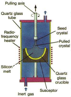
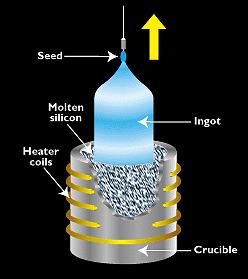
11 The Czochralski Process To grow crystals, one starts with very pure semiconductor grade silicon, which is melted in a quartz-lined graphite crucible. The melt is held at a temperature of 1690K, which is slightly greater than the melting point (1685K) of silicon. A precisely controlled quantity of the dopant is added to the melt The ratio of the concentration of impurities in the solid, C o to that in the liquid, C t, is known as the equilibrium segregation coefficient k o k o = C o /C l Seed Crystal After having set up the melt, a seed crystal (a small highly perfect crystal), attached to a holder and possessing the desired crystal orientation, is dipped into the melt and a small portion is allowed to melt. 11
12 12
13 13
 chip manufacture.")
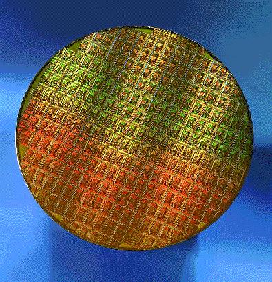
14 Here is a picture of a state-of-the-art 200 mm Si crystal as they are grown by the thousands for present day (2000) chip manufacture. 14


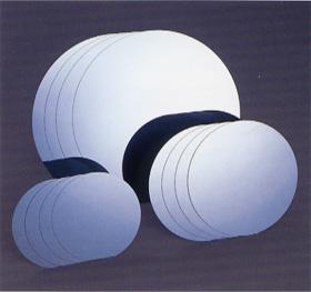
15 Ingot Slicing and Wafer Preparation In the final process, when the bulk of the melt has been grown, the crystal diameter is decreased until there is a point contact with the melt. The resulting ingot is cooled and removed to be made into wafers. The ingots have diameters as large as 200mm, with latest ones approaching 300mm. The ingot length is of the order of 100cm. 15

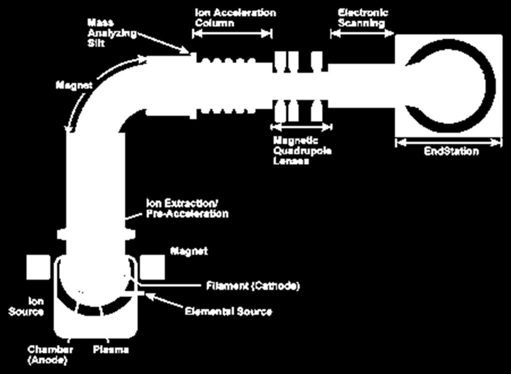
16 Slicing the wafers to be used in the fabrication of integrated circuits is a procedure that requires precision equipment. The object is to produce slices that are perfectly flat and as smooth as possible, with no damage to the crystal structure. The wafers need to be subjected to a number of steps known as lapping, polishing, and chemical etching. The wafers are cleaned, rinsed, and dried for use in the fabrication of discrete devices and integrated circuits 16
17 FABRICATION PROCESS Oxidation The process of oxidation consists of growing a thin film of silicon dioxide on the surface of the silicon wafer. Diffusion This process consists of the introduction of a few tenths to several micrometers of impurities by the solid-state diffusion of dopants into selected regions of a wafer to form junctions. Ion Implantation This is a process of introducing dopants into selected areas of the surface of the wafer by bombarding the surface with high-energy ions of the particular dopant. Photolithography In this process, the image on the reticle is transferred to the surface of the wafer. Epitaxy Epitaxy is the process of the controlled growth of a crystalline doped layer of silicon on a single crystal substrate. Metallization and interconnections After all semiconductor fabrication steps of a device or of an integrated circuit are completed, it becomes necessary to provide metallic interconnections for the 17 integrated circuit and for external connections to both the device and to the IC.

18 Silicon dioxide, as we shall see later, plays an important role in shielding of the surface so that dopant atoms, by diffusion or ion implantation, may be driven into other selected regions 18
19 19
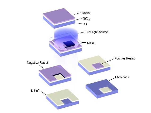
20 Etching Techniques Etching is the process of selective removal of regions of a semiconductor, metal, or silicon dioxide. There are two types of etchings: wet and dry In wet etching, the wafers are immersed in a chemical solution at a predetermined temperature. In this process, the material to be etched is removed equally in all directions so that some material is etched from regions where it is to be left. This becomes a serious problem when dealing with small dimensions. In dry (or plasma) etching, the wafers are immersed in a gaseous plasma created by a radio-frequency electric field applied to a gas such as argon. Electrons are initially released by field emission from an electrode. These electrodes gain kinetic energy from the field, collide with, and transfer energy to the gas molecules, which results in generating ions and electrons. The newly generated electrons collide with other gas molecules and the avalanche process continues throughout the gas, forming a plasma. The wafer to be etched is placed on an electrode and is subjected to the bombardment of its surface by gas ions. As a result, atoms at or near the surface to be etched are removed by the transfer of momentum from the ions to the atoms. 20
21 Diffusion Most of these diffusion processes occur in two steps: the predeposition and the drive-in diffusion. In the pre deposition step, a high concentration of dopant atoms are introduced at the silicon surface by a vapor that contains the dopant at a temperature of about 1000 C. In recent years Ion Implantation is used. At the temperature of l000 C,silicon atoms move out of their lattice sites creating a high density of vacancies and breaking the bond with the neighboring atoms. The second step is drive in process, used to drive the impurities deeper into the surface without adding anymore impurities. Common dopants are boron for P-type layers and phosphorus, antimony, and arsenic for N-type layers. A typical arrangement of the process of diffusion is shown in Figure. The wafers are placed in a quartz furnace tube that is heated by resistance heaters surrounding it. So that the wafers may be inserted and removed easily from the furnace, they are placed in a slotted quartz carrier known as a boat. To introduce a phosphorus dopant, as an example, phosphorus oxychloride 21
22 22
23 (POCI3) is placed in a container either inside the quartz tube, in a region of relatively low temperature, or in a container outside the furnace at a temperature that helps maintain its liquid form. Nitrogen and oxygen gas are made to pass over the container. These gases carry the dopant vapor into the furnace, where the gases are deposited on the surface of the wafers. These gases react with the silicon, forming a layer on the surface of the wafer that contains silicon, oxygen, and phosphorus. At the high temperature of the furnace, phosphorus diffuses easily into the silicon. Diffusion depth is controlled by the time and temperature of the drive-in process. By precise control of the time and temperature (to within 0.25 C),accurate junction depths of fraction of a micron can be obtained. 23
24 Ion Implantation To generate ions, such as those of phosphorus, an arc discharge is made to occur in a gas, such as phosphine (PH 3 ),that contains the dopant. The ions are then accelerated in an electric field so that they acquire an energy of about 20keV and are passed through a strong magnetic field. Because during the arc discharge unwanted impurities may have been generated, the magnetic field acts to separate these impurities from the dopant ions based on the fact that the amount of deflection of a particle in a magnetic field depends on its mass. Following the action of the magnetic field, the ions are further accelerated so that their energy reaches several hundred kev, whereupon they are focused on and strike the surface of the silicon wafer. 24
25 25
26 Advantages of Ion Implantation 1. Doping levels can be precisely controlled since the incident ion beam can be accurately measured as an electric current. 2. The depth of the dopant can be easily regulated by control of the incident ion velocity. It is capable of very shallow penetrations. 3. Extreme purity of the dopant is guaranteed. 4. The doping uniformity across the surface can be accurately controlled. 5. Because the ions enter the solid as a directed beam, there is very little spread of the beam, thus the doping area can be clearly defined. 6. Since this is a low-temperature process, the movement of impurities is minimized. 26

27 27
28 Photolithography 1. The wafer is baked at 100 C to solidify the resist on the wafer. 2. The reticle is placed on the wafer and aligned by computer control. 3. The reticle is exposed to ultraviolet light with the transparent parts of the reticle passing the light onto the wafer. The photoresist under the opaque regions of the reticle is unaffected. 4. The exposed photoresist is chemically removed by dissolving it in an organic solvent and exposing the silicon dioxide underneath. This is a process very similar to that used in developing photographic film. The exposed silicon dioxide is then etched away using hydrofluoric acid, which dissolves silicon dioxide and not silicon. The regions under the opaque part of the reticle are still covered by the silicon dioxide and the photoresist. The photoresist under the opaque regions of the reticle is stripped using a proper solvent and the silicon dioxide is exposed. 28
29 29


30 30
31 Deep UV Photolithography 31
32 Epitaxial Growth Epitaxy is used to deposit N on N+ silicon, which is impossible to accomplish by diffusion. It is also used in isolation between bipolar transistors wherein N- is deposited on P. We list below, and with reference to Figure, the sequence of operation involved in the process: 1. Heat wafer to 1200 C. 2. Turn on H 2 to reduce the SiO 2 on the wafer surface. 3. Turn on anhydrous HCl to vapor-etch the surface of the wafer. This removes a small amount of silicon and other contaminants. 4. Turn off HCl. 5. Drop temperature to 1100 C. 6. Turn on silicon tetrachloride (SiCl 4 ). 7. Introduce dopant. 32
33 33

34 Plasma- based ion implantation and film deposition system 34

35 4" Wafer after Metallization 35
36 36
37 Planar PN Junction Diode Fabrication Figure Process Description 1. An N+ substrate grown by the Czochralski process is the starting metal of approximatly 150μmthick. 2. A layer of N-type silicon (1-5μm) is grown on the substrate by epitaxy. 3. Silicon dioxide layer deposited by oxidation. 4. Surface is coated with photoresist (positive). 5. Mask is placed on surface of silicon, aligned, and exposed to UV light. 6. Mask is removed, resist is removed, and SiOz under the exposed resist is etched. 7. Boron is diffused to form P region. Boron diffuses easily in silicon but not in SiO 2 8. Thin aluminum film is deposited over surface. 9. Metallized area is covered with resist and another mask is used to identify areas where metal is to be preserved. Wafer is etched to remove unwanted metal. Resist is then dissolved. 10. Contact metal is deposited on the back surface and ohmic contacts are made by heat treatment. 37
38 38
39 39
40 40
Fabrication Process. Crystal Growth Doping Deposition Patterning Lithography Oxidation Ion Implementation CONCORDIA VLSI DESIGN LAB
 Fabrication Process Crystal Growth Doping Deposition Patterning Lithography Oxidation Ion Implementation 1 Fabrication- CMOS Process Starting Material Preparation 1. Produce Metallurgical Grade Silicon
ELEC 3908, Physical Electronics, Lecture 4. Basic Integrated Circuit Processing
 ELEC 3908, Physical Electronics, Lecture 4 Basic Integrated Circuit Processing Lecture Outline Details of the physical structure of devices will be very important in developing models for electrical behavior
The Physical Structure (NMOS)
") The Physical Structure (NMOS) Al SiO2 Field Oxide Gate oxide S n+ Polysilicon Gate Al SiO2 SiO2 D n+ L channel P Substrate Field Oxide contact Metal (S) n+ (G) L W n+ (D) Poly 1 3D Perspective 2 3 Fabrication
The Physical Structure (NMOS) Al SiO2 Field Oxide Gate oxide S n+ Polysilicon Gate Al SiO2 SiO2 D n+ L channel P Substrate Field Oxide contact Metal (S) n+ (G) L W n+ (D) Poly 1 3D Perspective 2 3 Fabrication
Microelettronica. Planar Technology for Silicon Integrated Circuits Fabrication. 26/02/2017 A. Neviani - Microelettronica
 Microelettronica Planar Technology for Silicon Integrated Circuits Fabrication 26/02/2017 A. Neviani - Microelettronica Introduction Simplified crosssection of an nmosfet and a pmosfet Simplified crosssection
PROCESS FLOW AN INSIGHT INTO CMOS FABRICATION PROCESS
 Contents: VI Sem ECE 06EC63: Analog and Mixed Mode VLSI Design PROCESS FLOW AN INSIGHT INTO CMOS FABRICATION PROCESS 1. Introduction 2. CMOS Fabrication 3. Simplified View of Fabrication Process 3.1 Alternative
Chapter 3 CMOS processing technology
 Chapter 3 CMOS processing technology (How to make a CMOS?) Si + impurity acceptors(p-type) donors (n-type) p-type + n-type => pn junction (I-V) 3.1.1 (Wafer) Wafer = A disk of silicon (0.25 mm - 1 mm thick),
Chapter 2 MOS Fabrication Technology
 Chapter 2 MOS Fabrication Technology Abstract This chapter is concerned with the fabrication of metal oxide semiconductor (MOS) technology. Various processes such as wafer fabrication, oxidation, mask
A discussion of crystal growth, lithography, etching, doping, and device structures is presented in
 Chapter 5 PROCESSING OF DEVICES A discussion of crystal growth, lithography, etching, doping, and device structures is presented in the following overview gures. SEMICONDUCTOR DEVICE PROCESSING: AN OVERVIEW
EE6303 LINEAR INTEGRATED CIRCUITS AND APPLICATIONS 2 MARK QUESTIONS WITH ANSWERS UNIT I IC FABRICATION
 SRI VENKATESWARA COLLEGE OF ENGINEERING AND TECHNOLOGY TIRUPACHUR DEPARTMENT OFELECTRICAL AND ELECTRONICS ENGINEERING EE6303 LINEAR INTEGRATED CIRCUITS AND APPLICATIONS 1. Define an Integrated circuit.
TOWARD MEMS!Instructor: Riadh W. Y. Habash
 TOWARD MEMS!Instructor: Riadh W. Y. Habash Students are presented with aspects of general production and manufacturing of integrated circuit (IC) products to enable them to better liaise with and participate
ECE 440 Lecture 27 : Equilibrium P-N Junctions I Class Outline:
 ECE 440 Lecture 27 : Equilibrium P-N Junctions I Class Outline: Fabrication of p-n junctions Contact Potential Things you should know when you leave Key Questions What are the necessary steps to fabricate
Silicon Manufacturing
 Silicon Manufacturing Group Members Young Soon Song Nghia Nguyen Kei Wong Eyad Fanous Hanna Kim Steven Hsu th Fundamental Processing Steps 1.Silicon Manufacturing a) Czochralski method. b) Wafer Manufacturing
Czochralski Crystal Growth
 Czochralski Crystal Growth Crystal Pulling Crystal Ingots Shaping and Polishing 300 mm wafer 1 2 Advantage of larger diameter wafers Wafer area larger Chip area larger 3 4 Large-Diameter Wafer Handling
Physics and Material Science of Semiconductor Nanostructures
 Physics and Material Science of Semiconductor Nanostructures PHYS 570P Prof. Oana Malis Email: omalis@purdue.edu Today Bulk semiconductor growth Single crystal techniques Nanostructure fabrication Epitaxial
This Appendix discusses the main IC fabrication processes.
 IC Fabrication B B.1 Introduction This Appendix discusses the main IC fabrication processes. B.2 NMOS fabrication NMOS transistors are formed in a p-type substrate. The NMOS fabrication process requires
Chapter 3 Silicon Device Fabrication Technology
 Chapter 3 Silicon Device Fabrication Technology Over 10 15 transistors (or 100,000 for every person in the world) are manufactured every year. VLSI (Very Large Scale Integration) ULSI (Ultra Large Scale
EE 330 Lecture 9. IC Fabrication Technology Part 2
 EE 330 Lecture 9 IC Fabrication Technology Part 2 Quiz 8 A 2m silicon crystal is cut into wafers using a wire saw. If the wire diameter is 220um and the wafer thickness is 350um, how many wafers will this
EECS130 Integrated Circuit Devices
 EECS130 Integrated Circuit Devices Professor Ali Javey 9/13/2007 Fabrication Technology Lecture 1 Silicon Device Fabrication Technology Over 10 15 transistors (or 100,000 for every person in the world)
Fabrication and Layout
 ECEN454 Digital Integrated Circuit Design Fabrication and Layout ECEN 454 3.1 A Glimpse at MOS Device Polysilicon Aluminum ECEN 475 4.2 1 Material Classification Insulators Glass, diamond, silicon oxide
Figure 2.3 (cont., p. 60) (e) Block diagram of Pentium 4 processor with 42 million transistors (2000). [Courtesy Intel Corporation.
 (e) Block diagram of Pentium 4 processor with 42 million transistors (2000). [Courtesy Intel Corporation.") Figure 2.1 (p. 58) Basic fabrication steps in the silicon planar process: (a) oxide formation, (b) selective oxide removal, (c) deposition of dopant atoms on wafer, (d) diffusion of dopant atoms into exposed
Figure 2.1 (p. 58) Basic fabrication steps in the silicon planar process: (a) oxide formation, (b) selective oxide removal, (c) deposition of dopant atoms on wafer, (d) diffusion of dopant atoms into exposed
EE 5344 Introduction to MEMS. CHAPTER 3 Conventional Si Processing
 3. Conventional licon Processing Micromachining, Microfabrication. EE 5344 Introduction to MEMS CHAPTER 3 Conventional Processing Why silicon? Abundant, cheap, easy to process. licon planar Integrated
CHAPTER - 4 CMOS PROCESSING TECHNOLOGY
 CHAPTER - 4 CMOS PROCESSING TECHNOLOGY Samir kamal Spring 2018 4.1 CHAPTER OBJECTIVES 1. Introduce the CMOS designer to the technology that is responsible for the semiconductor devices that might be designed
VLSI INTRODUCTION P.VIDYA SAGAR ( ASSOCIATE PROFESSOR) Department of Electronics and Communication Engineering, VBIT
 Department of Electronics and Communication Engineering, VBIT") VLSI INTRODUCTION P.VIDYA SAGAR ( ASSOCIATE PROFESSOR) contents UNIT I INTRODUCTION: Introduction to IC Technology MOS, PMOS, NMOS, CMOS & BiCMOS technologies. BASIC ELECTRICAL PROPERTIES : Basic Electrical
VLSI INTRODUCTION P.VIDYA SAGAR ( ASSOCIATE PROFESSOR) contents UNIT I INTRODUCTION: Introduction to IC Technology MOS, PMOS, NMOS, CMOS & BiCMOS technologies. BASIC ELECTRICAL PROPERTIES : Basic Electrical
PHYSICAL ELECTRONICS(ECE3540) Brook Abegaz, Tennessee Technological University, Fall 2013
 Brook Abegaz, Tennessee Technological University, Fall 2013") PHYSICAL ELECTRONICS(ECE3540) Brook Abegaz, Tennessee Technological University, Fall 2013 1 Chapter 1 The Crystal Structure of Solids Physical Electronics: Includes aspects of the physics of electron movement
PHYSICAL ELECTRONICS(ECE3540) Brook Abegaz, Tennessee Technological University, Fall 2013 1 Chapter 1 The Crystal Structure of Solids Physical Electronics: Includes aspects of the physics of electron movement
Lecture 22: Integrated circuit fabrication
 Lecture 22: Integrated circuit fabrication Contents 1 Introduction 1 2 Layering 4 3 Patterning 7 4 Doping 8 4.1 Thermal diffusion......................... 10 4.2 Ion implantation.........................
EE 330 Lecture 8. IC Fabrication Technology Part II. - Oxidation - Epitaxy - Polysilicon - Interconnects
 EE 330 Lecture 8 IC Fabrication Technology Part II - Oxidation - Epitaxy - Polysilicon - Interconnects Review from Last Time MOS Transistor Bulk Source Gate Drain p-channel MOSFET Lightly-doped n-type
Most semiconductor devices contain at least one junction between p-type and n-type material. These p-n junctions are fundamental to the performance
 Ch. 5: p-n Junction Most semiconductor devices contain at least one junction between p-type and n-type material. These p-n junctions are fundamental to the performance of functions such as rectification,
INTEGRATED-CIRCUIT TECHNOLOGY
 INTEGRATED-CIRCUIT TECHNOLOGY 0. Silicon crystal growth and wafer preparation 1. Processing Steps 1.1. Photolitography 1.2. Oxidation 1.3. Layer Deposition 1.4. Etching 1.5. Diffusion 1.6 Backend: assembly,
VLSI Digital Systems Design
 VLSI Digital Systems Design CMOS Processing cmpe222_03process_ppt.ppt 1 Si Purification Chemical purification of Si Zone refined Induction furnace Si ingot melted in localized zone Molten zone moved from
PY2N20 Material Properties and Phase Diagrams
 PY2N20 Material Properties and Phase Diagrams Lecture 9 P. Stamenov, PhD School of Physics, TCD PY2N20-9 Semiconductor Wafer Production - Si Czochralski Growth Growth from melt Melt 99.999999% pure polycrystalline
Microelectronics. Integrated circuits. Introduction to the IC technology M.Rencz 11 September, Expected decrease in line width
 Microelectronics Introduction to the IC technology M.Rencz 11 September, 2002 9/16/02 1/37 Integrated circuits Development is controlled by the roadmaps. Self-fulfilling predictions for the tendencies
VLSI Design and Simulation
 VLSI Design and Simulation CMOS Processing Technology Topics CMOS Processing Technology Semiconductor Processing How do we make a transistor? Fabrication Process Wafer Processing Silicon single crystal
Instructor: Dr. M. Razaghi. Silicon Oxidation
 SILICON OXIDATION Silicon Oxidation Many different kinds of thin films are used to fabricate discrete devices and integrated circuits. Including: Thermal oxides Dielectric layers Polycrystalline silicon
Semiconductor device fabrication
 REVIEW Semiconductor device fabrication is the process used to create the integrated circuits (silicon chips) that are present in everyday electrical and electronic devices. It is a multiplestep sequence
Microelectronic Device Instructional Laboratory. Table of Contents
 Introduction Process Overview Microelectronic Device Instructional Laboratory Introduction Description Flowchart MOSFET Development Process Description Process Steps Cleaning Solvent Cleaning Photo Lithography
EE 330 Lecture 9. IC Fabrication Technology Part II. -Oxidation -Epitaxy -Polysilicon -Planarization -Resistance and Capacitance in Interconnects
 EE 330 Lecture 9 IC Fabrication Technology Part II -Oxidation -Epitaxy -Polysilicon -Planarization -Resistance and Capacitance in Interconnects Review from Last Time IC Fabrication Technology Crystal Preparation
Ajay Kumar Gautam [VLSI TECHNOLOGY] VLSI Technology for 3RD Year ECE/EEE Uttarakhand Technical University
![Ajay Kumar Gautam [VLSI TECHNOLOGY] VLSI Technology for 3RD Year ECE/EEE Uttarakhand Technical University](/thumbs/75/72824557.jpg "Ajay Kumar Gautam [VLSI TECHNOLOGY] VLSI Technology for 3RD Year ECE/EEE Uttarakhand Technical University") 2014 Ajay Kumar Gautam [VLSI TECHNOLOGY] VLSI Technology for 3RD Year ECE/EEE Uttarakhand Technical University Page1 Syllabus UNIT 1 Introduction to VLSI Technology: Classification of ICs, Scale of integration,
2014 Ajay Kumar Gautam [VLSI TECHNOLOGY] VLSI Technology for 3RD Year ECE/EEE Uttarakhand Technical University Page1 Syllabus UNIT 1 Introduction to VLSI Technology: Classification of ICs, Scale of integration,
VLSI Technology. By: Ajay Kumar Gautam
 By: Ajay Kumar Gautam Introduction to VLSI Technology, Crystal Growth, Oxidation, Epitaxial Process, Diffusion Process, Ion Implantation, Lithography, Etching, Metallization, VLSI Process Integration,
Chapter 2 Crystal Growth and Wafer Preparation
 Chapter 2 Crystal Growth and Wafer Preparation Professor Paul K. Chu Advantages of Si over Ge Si has a larger bandgap (1.1 ev for Si versus 0.66 ev for Ge) Si devices can operate at a higher temperature
EE 5611 Introduction to Microelectronic Technologies Fall Tuesday, September 02, 2014 Lecture 01
 EE 5611 Introduction to Microelectronic Technologies Fall 2014 Tuesday, September 02, 2014 Lecture 01 1 Instructor: Jing Bai Contact Email: jingbai@d.umn.edu, hone: (218)726-8606, Office: MWAH 255 Webpage:
EE 5611 Introduction to Microelectronic Technologies Fall Tuesday, September 04, 2012 Lecture 01
 EE 5611 Introduction to Microelectronic Technologies Fall 2012 Tuesday, September 04, 2012 Lecture 01 1 Instructor: Jing Bai Contact Email: jingbai@d.umn.edu, hone: (218)726-8606, Office: MWAH 255 Webpage:
A trip inside a microchip: a sand grain with a big memory
 A trip inside a microchip: a sand grain with a big memory Francesca di Monte, Associazione Culturale Chimicare francescadimonte@hotmail.com Prior to 1971, a computer unit was a huge machine, requiring
Semiconductor Device Fabrication
 5 May 2003 Review Homework 6 Semiconductor Device Fabrication William Shockley, 1945 The network before the internet Bell Labs established a group to develop a semiconductor replacement for the vacuum
Crystal Growth and Wafer Fabrication. K.Sivasankaran, Assistant Professor (Senior), VLSI Division, School of Electronics Engineering, VIT
, VLSI Division, School of Electronics Engineering, VIT") Crystal Growth and Wafer Fabrication K.Sivasankaran, Assistant Professor (Senior), VLSI Division, School of Electronics Engineering, VIT Crystal growth Obtaining sand Raw Polysilicon Czochralski Process
Crystal Growth and Wafer Fabrication K.Sivasankaran, Assistant Professor (Senior), VLSI Division, School of Electronics Engineering, VIT Crystal growth Obtaining sand Raw Polysilicon Czochralski Process
PROCESSING OF INTEGRATED CIRCUITS
 PROCESSING OF INTEGRATED CIRCUITS Overview of IC Processing (Part I) Silicon Processing Lithography Layer Processes Use in IC Fabrication (Part II) Integrating the Fabrication Steps IC Packaging (Part
KGC SCIENTIFIC Making of a Chip
 KGC SCIENTIFIC www.kgcscientific.com Making of a Chip FROM THE SAND TO THE PACKAGE, A DIAGRAM TO UNDERSTAND HOW CPU IS MADE? Sand CPU CHAIN ANALYSIS OF SEMICONDUCTOR Material for manufacturing process
Lecture 19 Microfabrication 4/1/03 Prof. Andy Neureuther
 EECS 40 Spring 2003 Lecture 19 Microfabrication 4/1/03 Prof. ndy Neureuther How are Integrated Circuits made? Silicon wafers Oxide formation by growth or deposition Other films Pattern transfer by lithography
HOMEWORK 4 and 5. March 15, Homework is due on Monday March 30, 2009 in Class. Answer the following questions from the Course Textbook:
 HOMEWORK 4 and 5 March 15, 2009 Homework is due on Monday March 30, 2009 in Class. Chapter 7 Answer the following questions from the Course Textbook: 7.2, 7.3, 7.4, 7.5, 7.6*, 7.7, 7.9*, 7.10*, 7.16, 7.17*,
Wafer (1A) Young Won Lim 4/30/13
 Young Won Lim 4/30/13") Copyright (c) 2011-2013 Young W. Lim. Permission is granted to copy, distribute and/or modify this document under the terms of the GNU Free Documentation License, Version 1.2 or any later version published
Copyright (c) 2011-2013 Young W. Lim. Permission is granted to copy, distribute and/or modify this document under the terms of the GNU Free Documentation License, Version 1.2 or any later version published
BASICS OF MANUFACTURING INTEGRATED CIRCUITS
 BASICS OF MANUFACTURING INTEGRATED CIRCUITS Opportunities for filtration exist for the manufacture of very small electronic components referred to as semiconductors. This broad category includes devices
EE40 Lec 22. IC Fabrication Technology. Prof. Nathan Cheung 11/19/2009
 Suggested Reading EE40 Lec 22 IC Fabrication Technology Prof. Nathan Cheung 11/19/2009 300mm Fab Tour http://www-03.ibm.com/technology/manufacturing/technology_tour_300mm_foundry.html Overview of IC Technology
Chapter 2 Manufacturing Process
 Digital Integrated Circuits A Design Perspective Chapter 2 Manufacturing Process 1 CMOS Process 2 CMOS Process (n-well) Both NMOS and PMOS must be built in the same silicon material. PMOS in n-well NMOS
EE 434 Lecture 9. IC Fabrication Technology
 EE 434 Lecture 9 IC Fabrication Technology Quiz 7 The layout of a film resistor with electrodes A and B is shown. If the sheet resistance of the film is 40 /, determine the resistance between nodes A and
EE 330 Lecture 8. IC Fabrication Technology Part II. - Masking - Photolithography - Deposition - Etching - Diffusion
 EE 330 Lecture 8 IC Fabrication Technology Part II?? - Masking - Photolithography - Deposition - Etching - Diffusion Review from Last Time Technology Files Provide Information About Process Process Flow
Process Flow in Cross Sections
 Process Flow in Cross Sections Process (simplified) 0. Clean wafer in nasty acids (HF, HNO 3, H 2 SO 4,...) --> wear gloves! 1. Grow 500 nm of SiO 2 (by putting the wafer in a furnace with O 2 2. Coat
Complexity of IC Metallization. Early 21 st Century IC Technology
 EECS 42 Introduction to Digital Electronics Lecture # 25 Microfabrication Handout of This Lecture. Today: how are Integrated Circuits made? Silicon wafers Oxide formation by growth or deposition Other
Microstructure of Electronic Materials. Amorphous materials. Single-Crystal Material. Professor N Cheung, U.C. Berkeley
 Microstructure of Electronic Materials Amorphous materials Single-Crystal Material 1 The Si Atom The Si Crystal diamond structure High-performance semiconductor devices require defect-free crystals 2 Crystallographic
IC/MEMS Fabrication - Outline. Fabrication
 IC/MEMS Fabrication - Outline Fabrication overview Materials Wafer fabrication The Cycle: Deposition Lithography Etching Fabrication IC Fabrication Deposition Spin Casting PVD physical vapor deposition
Microfabrication of Integrated Circuits
 Microfabrication of Integrated Circuits OUTLINE History Basic Processes Implant; Oxidation; Photolithography; Masks Layout and Process Flow Device Cross Section Evolution Lecture 38, 12/05/05 Reading This
1. Introduction. What is implantation? Advantages
 Ion implantation Contents 1. Introduction 2. Ion range 3. implantation profiles 4. ion channeling 5. ion implantation-induced damage 6. annealing behavior of the damage 7. process consideration 8. comparison
Mostafa Soliman, Ph.D. May 5 th 2014
 Mostafa Soliman, Ph.D. May 5 th 2014 Mostafa Soliman, Ph.D. 1 Basic MEMS Processes Front-End Processes Back-End Processes 2 Mostafa Soliman, Ph.D. Wafers Deposition Lithography Etch Chips 1- Si Substrate
Making of a Chip Illustrations
 Making of a Chip Illustrations 22nm 3D/Trigate Transistors Version April 2015 1 The illustrations on the following foils are low resolution images that visually support the explanations of the individual
Semiconductor Manufacturing Technology. Semiconductor Manufacturing Technology
 Semiconductor Manufacturing Technology Michael Quirk & Julian Serda October 2001 by Prentice Hall Chapter 17 Doping Processes Common Dopants Used in Semiconductor Manufacturing Acceptor Dopant Group IIIA
Semiconductor Technology
 Semiconductor Technology from A to Z Oxidation www.halbleiter.org Contents Contents List of Figures List of Tables II III 1 Oxidation 1 1.1 Overview..................................... 1 1.1.1 Application...............................
EE 330 Lecture 9. IC Fabrication Technology Part II. -Oxidation -Epitaxy -Polysilicon -Planarization -Resistance and Capacitance in Interconnects
 EE 330 Lecture 9 IC Fabrication Technology Part II -Oxidation -Epitaxy -Polysilicon -Planarization -Resistance and Capacitance in Interconnects Review from Last Time Etching Dry etch (anisotropic) SiO
PHYS 534 (Fall 2008) Process Integration OUTLINE. Examples of PROCESS FLOW SEQUENCES. >Surface-Micromachined Beam
 Process Integration OUTLINE. Examples of PROCESS FLOW SEQUENCES. >Surface-Micromachined Beam") PHYS 534 (Fall 2008) Process Integration Srikar Vengallatore, McGill University 1 OUTLINE Examples of PROCESS FLOW SEQUENCES >Semiconductor diode >Surface-Micromachined Beam Critical Issues in Process
PHYS 534 (Fall 2008) Process Integration Srikar Vengallatore, McGill University 1 OUTLINE Examples of PROCESS FLOW SEQUENCES >Semiconductor diode >Surface-Micromachined Beam Critical Issues in Process
IC Fabrication Technology Part III Devices in Semiconductor Processes
 EE 330 Lecture 10 IC Fabrication Technology Part III Metalization and Interconnects Parasitic Capacitances Back-end Processes Devices in Semiconductor Processes Resistors Diodes Review from Last Lecture
Schematic creation of MOS field effect transistor.
 Schematic creation of MOS field effect transistor. Gate electrode Drain electrode Source electrode Gate oxide Gate length Page 1 Step 0 The positively doped silicon wafer is first coated with an insulating
Thermal Evaporation. Theory
 Thermal Evaporation Theory 1. Introduction Procedures for depositing films are a very important set of processes since all of the layers above the surface of the wafer must be deposited. We can classify
Chapter 5 Thermal Processes
 Chapter 5 Thermal Processes 1 Topics Introduction Hardware Oxidation Diffusion Annealing Post-Implantation Alloying Reflow High Temp CVD Epi Poly Silicon Nitride RTP RTA RTP Future Trends 2 Definition
Department of Electrical Engineering. Jungli, Taiwan
 Chapter 3 Fabrication of CMOS Integrated Circuits Jin-Fu Li Department of Electrical Engineering National Central University Jungli, Taiwan Background Outline The CMOS Process Flow Design Rules Latchup
FABRICATION of MOSFETs
 FABRICATION of MOSFETs CMOS fabrication sequence -p-type silicon substrate wafer -creation of n-well regions for pmos transistors, -impurity implantation into the substrate. -thick oxide is grown in the
CRYSTAL GROWTH, WAFER FABRICATION AND BASIC PROPERTIES OF Si WAFERS- Chapter 3. Crystal Structure z a
 CRYSTAL GROWTH, WAFER FABRICATION AND BASIC PROPERTIES OF Si WAFERS- Chapter 3 Crystal Growth, Si Wafers- Chapter 3 z a C y B z a y Crystal Structure z a y Crystals are characterized by a unit cell which
Processing of Semiconducting Materials Prof. Pallab Banerjee Department of Material Science Indian Institute of Technology, Kharagpur
 Processing of Semiconducting Materials Prof. Pallab Banerjee Department of Material Science Indian Institute of Technology, Kharagpur Lecture - 35 Oxidation I (Refer Slide Time: 00:24) Today s topic of
Lecture 0: Introduction
 Lecture 0: Introduction Introduction Integrated circuits: many transistors on one chip. Very Large Scale Integration (VLSI): bucketloads! Complementary Metal Oxide Semiconductor Fast, cheap, low power
EE CRYSTAL GROWTH, WAFER FABRICATION AND BASIC PROPERTIES OF Si WAFERS- Chapter 3. Crystal Structure z a
 1 EE 1 FALL 1999-00 CRYSTAL GROWTH, WAFER FABRICATION AND BASIC PROPERTIES OF Si WAFERS- Chapter 3 z a B Crystal Structure z a z a C y y y A x x Cubic BCC FCC x Crystals are characterized by a unit cell
LANDOLT-BÖRNSTEIN. Zahlenwerte und Funktionen aus Naturwissenschaften und Technik. Neue Serie. Gesamtherausgabe: K.-H. Hellwege O.
 LANDOLT-BÖRNSTEIN Zahlenwerte und Funktionen aus Naturwissenschaften und Technik Neue Serie Gesamtherausgabe: K.-H. Hellwege O. Madelung Gruppe III: Kristall- und Festkörperphysik Band 17 Halbleiter Herausgeber:
Fabrication Technology, Part I
 EEL5225: Principles of MEMS Transducers (Fall 2003) Fabrication Technology, Part I Agenda: Oxidation, layer deposition (last lecture) Lithography Pattern Transfer (etching) Impurity Doping Reading: Senturia,
Introduction to CMOS VLSI Design. Layout, Fabrication, and Elementary Logic Design
 Introduction to CMOS VLSI Design Layout, Fabrication, and Elementary Logic Design CMOS Fabrication CMOS transistors are fabricated on silicon wafer Lithography process similar to printing press On each
Chapter 4. UEEP2613 Microelectronic Fabrication. Oxidation
 Chapter 4 UEEP2613 Microelectronic Fabrication Oxidation Prepared by Dr. Lim Soo King 24 Jun 2012 Chapter 4...113 Oxidation...113 4.0 Introduction... 113 4.1 Chemistry of Silicon Dioxide Formation... 115
Doping and Oxidation
 Technische Universität Graz Institute of Solid State Physics Doping and Oxidation Franssila: Chapters 13,14, 15 Peter Hadley Technische Universität Graz Institute of Solid State Physics Doping Add donors
Lecture #18 Fabrication OUTLINE
 Transistors on a Chip Lecture #18 Fabrication OUTLINE IC Fabrication Technology Introduction the task at hand Doping Oxidation Thin-film deposition Lithography Etch Lithography trends Plasma processing
Technology. Semiconductor Manufacturing. Hong Xiao INTRODUCTION TO SECOND EDITION SPIE PRESS
 INTRODUCTION TO Semiconductor Manufacturing Technology SECOND EDITION Hong Xiao TECHNISCHE INFORMATIONSBiBUOTHEK UNIVERSITATSBIBLIOTHEK HANNOVER SPIE PRESS Bellingham,Washington USA Contents Preface to
Physical Vapor Deposition (PVD) Zheng Yang
 Zheng Yang") Physical Vapor Deposition (PVD) Zheng Yang ERF 3017, email: yangzhen@uic.edu Page 1 Major Fabrication Steps in MOS Process Flow UV light Mask oxygen Silicon dioxide photoresist exposed photoresist oxide
Physical Vapor Deposition (PVD) Zheng Yang ERF 3017, email: yangzhen@uic.edu Page 1 Major Fabrication Steps in MOS Process Flow UV light Mask oxygen Silicon dioxide photoresist exposed photoresist oxide
CS/ECE 5710/6710. N-type Transistor. N-type from the top. Diffusion Mask. Polysilicon Mask. CMOS Processing
 CS/ECE 5710/6710 CMOS Processing Addison-Wesley N-type Transistor D G +Vgs + Vds S N-type from the top i electrons - Diffusion Mask Mask for just the diffused regions Top view shows patterns that make
Lecture 2 Silicon Properties and Growth
 Lecture 2 Silicon Properties and Growth Chapters 1 & 2 Wolf and Tauber 1/63 Lecture 2 Why Silicon? Crystal Structure. Defects. Sand to Electronic Grade Polysilicon. Polycrystalline to Single Crystal Silicon.
Technology process. It s very small world. Electronics and Microelectronics AE4B34EM. Why is the integration so beneficial?
 It s very small world Electronics and Microelectronics AE4B34EM 9. lecture IC processing technology Wafer fabrication Lithography How to get 1 000 000 000 Components to 1 cm 2 Human hair on the surface
CHAPTER 1 HOW SEMICONDUCTOR CHIPS ARE MADE
 CHAPTER 1 HOW SEMICONDUCTOR CHIPS ARE MADE Hwaiyu Geng Hewlett-Packard Company Palo Alto, California Lin Zhou Intel Corporation Hillsboro, Oregon 1.1 INTRODUCTION Over the past decades, an information
Metallization deposition and etching. Material mainly taken from Campbell, UCCS
 Metallization deposition and etching Material mainly taken from Campbell, UCCS Application Metallization is back-end processing Metals used are aluminum and copper Mainly involves deposition and etching,
The lowest quality of silicon is the so- called metallurgical silicon. The source material of making metallurgical silicon is quartzite.
 ET3034TUx - 4.2 - Manufacturing of crystalline silicon We have various types of silicon wafers such as monocrystalline silicon and polycrystalline silicon. In this block I will give an answer to the question:
CMOS VLSI Design. Introduction. All materials are from the textbook Weste and Harris, 3 rd Edition CMOS VLSI DESIGN. Introduction
 CMOS VLSI Design Introduction ll materials are from the textbook Weste and Harris, 3 rd Edition CMOS VLSI DESIGN Introduction Chapter previews the entire field, subsequent chapters elaborate on specific
Manufacturing Technologies for MEMS and SMART SENSORS
 4 Manufacturing Technologies for MEMS and SMART SENSORS Dr. H. K. Verma Distinguished Professor (EEE) Sharda University, Greater Noida (Formerly: Deputy Director and Professor of Instrumentation Indian
Semiconductor Optical Communication Components and Devices Lecture 8: Epitaxial growth - I (Techniques)
") Semiconductor Optical Communication Components and Devices Lecture 8: Epitaxial growth - I (Techniques) Prof. Utpal Das Professor, Department of Electrical Engineering, Laser Technology Program, Indian
Semiconductor Optical Communication Components and Devices Lecture 8: Epitaxial growth - I (Techniques) Prof. Utpal Das Professor, Department of Electrical Engineering, Laser Technology Program, Indian
Low Power VLSI Circuits and Systems Prof. Ajit Pal Department of Computer Science and Engineering Indian Institute of Technology, Kharagpur
 Low Power VLSI Circuits and Systems Prof. Ajit Pal Department of Computer Science and Engineering Indian Institute of Technology, Kharagpur Lecture No. # 02 MOS Transistors - I Hello and welcome to today
Silicon Wafer Processing PAKAGING AND TEST
 Silicon Wafer Processing PAKAGING AND TEST Parametrical test using test structures regularly distributed in the wafer Wafer die test marking defective dies dies separation die fixing (not marked as defective)
CMOS Technology. Flow varies with process types & company. Start with substrate selection. N-Well CMOS Twin-Well CMOS STI
 CMOS Technology Flow varies with process types & company N-Well CMOS Twin-Well CMOS STI Start with substrate selection Type: n or p Doping level, resistivity Orientation, 100, or 101, etc Other parameters
FABRICATION ENGINEERING MICRO- NANOSCALE ATTHE AND. Fourth Edition STEPHEN A. CAMPBELL. of Minnesota. University OXFORD UNIVERSITY PRESS
 AND FABRICATION ENGINEERING ATTHE MICRO- NANOSCALE Fourth Edition STEPHEN A. CAMPBELL University of Minnesota New York Oxford OXFORD UNIVERSITY PRESS CONTENTS Preface xiii prrt i OVERVIEW AND MATERIALS
CHAPTER 4: Oxidation. Chapter 4 1. Oxidation of silicon is an important process in VLSI. The typical roles of SiO 2 are:
 Chapter 4 1 CHAPTER 4: Oxidation Oxidation of silicon is an important process in VLSI. The typical roles of SiO 2 are: 1. mask against implant or diffusion of dopant into silicon 2. surface passivation
CMOS Manufacturing process. Design rule set
 CMOS Manufacturing process Circuit design Set of optical masks Fabrication process Circuit designer Design rule set Process engineer All material: Chap. 2 of J. Rabaey, A. Chandrakasan, B. Nikolic, Digital
VLSI. Lecture 1. Jaeyong Chung System-on-Chips (SoC) Laboratory Incheon National University. Based on slides of David Money Harris
 Laboratory Incheon National University. Based on slides of David Money Harris") VLSI Lecture 1 Jaeyong Chung System-on-Chips (SoC) Laboratory Incheon National University Based on slides of David Money Harris Goals of This Course Learn the principles of VLSI design Learn to design
VLSI Lecture 1 Jaeyong Chung System-on-Chips (SoC) Laboratory Incheon National University Based on slides of David Money Harris Goals of This Course Learn the principles of VLSI design Learn to design