Micro and nano structuring of carbon based materials for micro injection moulding and hot embossing
|
|
|
- MargaretMargaret Thompson
- 6 years ago
- Views:
Transcription
1 Micro and nano structuring of carbon based materials for micro injection moulding and hot embossing Victor Usov, Graham Cross, Neal O Hara, Declan Scanlan, Sander Paulen, Chris de Ruijter, Daniel Vlasveld, Jan Edelmann, Bernd Gründig FaBiMed Workshop, EuSPEN 30 May 2016 Nottingham The work leading to these results has received funding from the European Union Seventh Framework Programme FP7/ under Grant Agreement N Lead: Pablo Romero, AIMEN 1
2 Overview DLC as enabling material for mould fabrication Introduction to ion implant mask die forming technology Process development for fabrication of micro/nano features on mould Placing micro/nano features on industrial moulds Demonstration of replication by injection molding and hot embossing Conclusions 2

3 Diamond like carbon (DLC) material Amorphous, smooth Low cost relative to diamond 3


4 DLC mechanical applications Hard disk coating Steel razor blade coating 4
5 DLC as enabling material for mould fabrication The benefit of using DLC coating for moulding: Smooth conformal coatings from nm to tens of µm thickness Low surface energy Low polymer-tool adhesion and friction Inert and very resistant to wet chemistry Highly wear resistant Low thermal expansion and high elastic modulus Mature and optimized coating technology Multiple sources of DLC coatings available Strong adhesion to tooling steel 5


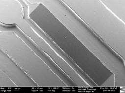
6 Molded PMMA using DLC coated Si mold : 18 th operation The research has shown that the ac:h coatings are robust, and advantageous in terms of reducing the inherent forces during demoulding. Further process optimisation is necessary Molded PMMA to widen the application area and using also to make possible the deposition of single and uncoated Si multiple features with a high mold : 3 rd degree of accuracy. operation 6
7 DLC as enabling material for mould fabrication These properties have an impact: Reducing de-moulding force (eg. 40% ABS) Improved feature quality and integrity Enhanced die lifetime and reusability Protection of the underlying machine metal features Potential for removal of polymer residue or build-up via wet chemistry without impacting feature size Potential for mould reuse: If the coating is used to a point where feature size is impacted, entire coating can be plasma or thermally removed and small features restored. Technical papers: Microinjection Moulding of Enchanced Thermoplastics, Monica Oliveira et al, Department of Mechanical Engineering, University of Aveiro, Portugal. Investigation of surface treatment effects in micro-injection-moulding, C.A.Griffiths et al, Int. J. Adv. Manuf. Technol., 47, (2009) A novel texturing of micro injection moulding tools by applying an amorphous hydrogenated carbon coating, C.A.Criffiths et al, Surf. Coating Tech., 235, (2013). 7


, EU")
8 Patterning technology: Top surface mask G. L. W. Cross, et. al., Process and System for Fabrication of Patterns on a Surface, US 8,524,100 (2013), EU Nationalization (2015) 8
9 Diamond AFM Probes: Lateral resolution for pillars down to 5.0 nm 5 nm 9


10 Diamond AFM Probes: Lateral resolution for pillars down to 5.0 nm 5 nm Tip Dimension 15nm x 125nm 10


11 Diamond AFM probes diamond probes Adama Super Sharp 2 nm tip radius Standard Si chip Diamond coated Si cantilever Diamond coated tip Single crystal apex Diamond atomic lattice fringes Super sharp diamond February Wafer scale diamond probe production 11


12 Diamond Flat Punch Probes: 12 2 um diameter; AR 1:1.5; Vertical side sides


13 Ion implant lithography and DLC coated moulds Steel Die or Mould Hard Coating Die or Mould Product Replication Hot Embossing Cold Forging Injection Moulding Nano-scale pattern by Ion Implant Patterning Technology Benefits : Smooth, featureless canvas No need for shims : Pattern integrated directly into mould Takes advantage of mould-protective coating feature 13
14 Patterning Technology Advantages Separation of patterning and material removal: Multi-scale technique: nm to 100 µm features over cm range areas E-beam comparable throughput Top-surface mask: Resistless Direct write on the mould: Patterns can be placed on non-planar surfaces of irregular shape High Performance Mask: High relief/aspect ratio small features can be produced Grey-scale: Placing patterns of different height on the same mould 5x5 mm Can be used in combination with conventional machining techniques such as mechanical milling and laser machining Complementary to steel die protective coatings 14

 Devices to be Fabricated : Microfluidics (POC diagnostics) Microneedles (Drug delivery) Materials : Glass,")
15 Technology development for replication in polymers Development of this technology was part of Fabrication of Medical Devices FaBiMed project Demonstrator medical devices with sub 10 µm features are to be fabricated by embossing/ injection moulding Pattern geometry and dimensions were inspired by medical microfluidic device specification (SensLab) Devices to be Fabricated : Microfluidics (POC diagnostics) Microneedles (Drug delivery) Materials : Glass, Polymer, Ceramics 15


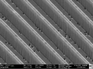
16 Technology development 2.0 um high relief IM by Promold Width = 2.5 um Space = 1.5 um 6.0 and 7.0 um high relief IM by Promold 6.0 um high relief HE by Fraunhofer Full Channels coverage Solid square Width = 4 um Space = 7 um Width = 1.2 um Pitch = 4, 8, 12 um IM/HE moulds were machined by Fraunhofer and DLC coated by Adama (16)

17 Technology development Step µm relief DLC/Si(100) Step µm relief DLC/St. Steel 0.5 µm 3.2 µm 6.8 µm 1.7 µm 4 µm 2.5 µm Step µm relief DLC/St. Steel or Al Step µm relief DLC/St. Steel; AR 18:1 1.2 µm 8.8 µm 0.5 µm µm

18 Technology development Step µm relief DLC/Si(100) Step µm relief DLC/St. Steel 0.5 µm 3.2 µm 6.8 µm 1.7 µm 4 µm 2.5 µm Step µm relief DLC/St. Steel or Al Step µm relief DLC/St. Steel; AR 18:1 0.5 µm 1.2 µm 8.8 µm µm
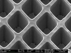
19 Highlights of technology development Achieved height of relief of 9 µm for 0.5 micron sized features: AR 16:1 Straight edges and side walls, write fields of 200 x 200 µm Ga mask removal, smooth finish Throughput for FIB process 0.2 to 1.0 mm 2 /hour depending on the pattern complexity and desired relief Throughput can be improved by a factor of 4 by using higher FIB current and improvement to the design layout Good correlation between dimensions of masked and etched features for low relief For higher relief, increase in height of relief comes at the expense of lateral dimensions etched features are narrower than implanted due to erosion of mask sides: Process maps have been established 19


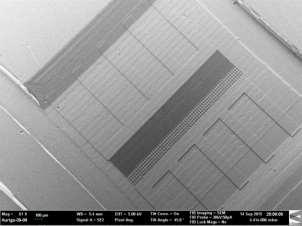
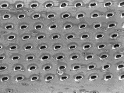
20 Placing micro/nano structures on a microfluidic mould C.A. Griffiths (U. Manchester) 80 nm pillar diameter 250 nm grating Complex mould shape: Small features of different height and scale placed in different areas on the same mould of irregular shape 4 mm 217nm 410 nm 78 nm 20

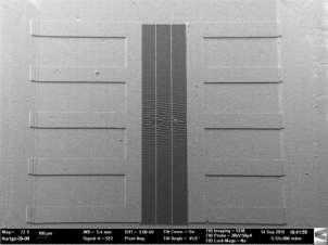
21 Small feature fabrication on DLC coated industrial moulds 3x3 mm 2 3x3 mm um 1.0 um 10 um 3x0.5 mm 2 (21)


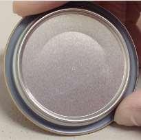
22 Replication by cold/warm forging Security/visual effect holograms on coins: Pore formation on epoxy coating: 100 nm 22


 9")

23 Replication by injection compression moulding Promold Arburg 25 ton injection molding machine IM by Promold on 250 µm thick lab-on-a-chip blanks Material: PPC- Polypropylene Random Copolymer (Moplen RP 7590) 9 µm relief Full replication of 32x32 µm features Partial replication of 9x9 µm features 23

 8 µm relief;")


24 Replication by hot embossing Reproducible hot embossing in 0.25 mm thick PC (Fraunhofer) 8 µm relief; full replication High vertical and side pattern fidelity Complete cavity filling Temperature 209 C, force 11.3 kn, time 480 s 24
25 Conclusions 1. DLC coatings are effective and helpful for IM and HE moulds 2. A new technology has been developed that demonstrates micro and nano-patterns fabrication into DLC coating directly on industrial silicon, steel and aluminium moulds 3. High quality replication by injection molding and hot embossing has been demonstrated 4. Higher stress cold/warm forging has also been demonstrated 5. Future work planned in order to evaluated the limits of this technology Limits of resolution Line edge roughness improvement Mould lifetime vs. feature size Throughout optimization 25
Polymer Microfabrication (Part II) Prof. Tianhong Cui, Mechanical Engineering ME 8254
 Prof. Tianhong Cui, Mechanical Engineering ME 8254") Polymer Microfabrication (Part II) Prof. Tianhong Cui, Mechanical Engineering ME 8254 Other Polymer Techniques Embossing Low cost High throughput Structures as small as 25 nm Injection molding Features
Polymer Microfabrication (Part II) Prof. Tianhong Cui, Mechanical Engineering ME 8254 Other Polymer Techniques Embossing Low cost High throughput Structures as small as 25 nm Injection molding Features
Micro-Nano Fabrication Research
 Micro-Nano Fabrication Research Technical Education Quality Improvement Programme 22-23 December 2014 Dr. Rakesh G. Mote Assistant Professor Department of Mechanical Engineering IIT Bombay rakesh.mote@iitb.ac.in;
Advanced Polymers And Resists For Nanoimprint Lithography
 Q U A L I T Y A S S U R A N C E MICROSYSTEMS & NANOSYSTEMS SPECIAL REPORT Advanced Polymers And Resists For Nanoimprint Lithography Numerous polymer systems specifically designed for nanoimprint lithography
Thin. Smooth. Diamond.
 UNCD Wafers Thin. Smooth. Diamond. UNCD Wafers - A Family of Diamond Material UNCD is Advanced Diamond Technologies (ADT) brand name for a family of thin fi lm diamond products. UNCD Aqua The Aqua series
Thin. Smooth. Diamond.
 UNCD Wafers Thin. Smooth. Diamond. UNCD Wafers - A Family of Diamond Material UNCD is Advanced Diamond Technologies (ADT) brand name for a family of thin fi lm diamond products. UNCD Aqua The Aqua series
Tribomechanical Properties of DLC Coatings Deposited by Magnetron Sputtering on Metallic and Insulating Substrates
 Tribomechanical Properties of DLC Coatings Deposited by Magnetron Sputtering on Metallic and Insulating Substrates Dr. Iván Fernández Martínez Indianapolis, May 10th, 2016 Diamond Like Carbon (DLC) Diamond-like
Micro-Electro-Mechanical Systems (MEMS) Fabrication. Special Process Modules for MEMS. Principle of Sensing and Actuation
 Fabrication. Special Process Modules for MEMS. Principle of Sensing and Actuation") Micro-Electro-Mechanical Systems (MEMS) Fabrication Fabrication Considerations Stress-Strain, Thin-film Stress, Stiction Special Process Modules for MEMS Bonding, Cavity Sealing, Deep RIE, Spatial forming
Micro-Electro-Mechanical Systems (MEMS) Fabrication Fabrication Considerations Stress-Strain, Thin-film Stress, Stiction Special Process Modules for MEMS Bonding, Cavity Sealing, Deep RIE, Spatial forming
Precision Electroforming in High-Strength NiColoy
 Taking the Stress out of Electroforming www.nicoform.com Precision Electroforming in High-Strength NiColoy Copyright 2007 NiCoForm, Inc. (Rochester, NY) Electroforming What is it? What is it good for?
Fabrication and application of high quality diamond coated. CMP pad conditioners
 Fabrication and application of high quality diamond coated CMP pad conditioners Hua Wang 1,a, Fanghong Sun 1,b* 1 School of Mechanical Engineering, Shanghai Jiao Tong University, Shanghai, 200240, China
Synthesis of diamond-like carbon films with super-low friction and wear properties
 Synthesis of diamond-like carbon films with super-low friction and wear properties MSE 676 All Things Carbon / 09-29-2009 A. Erdemir, O.L. Eryilmaz, and G. Fenske J. Vac. Sci. Technol. A 18(4), Jul/Aug
Nanoimprinting in Polymers and Applications in Cell Studies. Albert F. YEE Chemical Engineering & Materials Science UC Irvine
 Nanoimprinting in Polymers and Applications in Cell Studies Albert F. YEE Chemical Engineering & Materials Science UC Irvine Presentation outline Motivation Reversal imprinting Soft inkpad imprinting on
Micro-Electro-Mechanical Systems (MEMS) Fabrication. Special Process Modules for MEMS. Principle of Sensing and Actuation
 Fabrication. Special Process Modules for MEMS. Principle of Sensing and Actuation") Micro-Electro-Mechanical Systems (MEMS) Fabrication Fabrication Considerations Stress-Strain, Thin-film Stress, Stiction Special Process Modules for MEMS Bonding, Cavity Sealing, Deep RIE, Spatial forming
Micro-Electro-Mechanical Systems (MEMS) Fabrication Fabrication Considerations Stress-Strain, Thin-film Stress, Stiction Special Process Modules for MEMS Bonding, Cavity Sealing, Deep RIE, Spatial forming
Why Probes Look the Way They Do Concepts and Technologies of AFM Probes Manufacturing
 Agilent Technologies AFM e-seminar: Understanding and Choosing the Correct Cantilever for Your Application Oliver Krause NanoWorld Services GmbH All mentioned company names and trademarks are property
Alternative MicroFabrication and Applications in Medicine and Biology
 Alternative MicroFabrication and Applications in Medicine and Biology Massachusetts Institute of Technology 6.152 - Lecture 15 Fall 2003 These slides prepared by Dr. Hang Lu Outline of Today s Materials
Advanced Manufacturing Choices
 Advanced Manufacturing Choices Table of Content Mechanical Removing Techniques Ultrasonic Machining (USM) Sputtering and Focused Ion Beam Milling (FIB) Ultrasonic Machining In ultrasonic machining (USM),
General Introduction to Microstructure Technology p. 1 What is Microstructure Technology? p. 1 From Microstructure Technology to Microsystems
 General Introduction to Microstructure Technology p. 1 What is Microstructure Technology? p. 1 From Microstructure Technology to Microsystems Technology p. 9 The Parallels to Microelectronics p. 15 The
Outline. Introduction to the LIGA Microfabrication Process. What is LIGA? The LIGA Process. Dr. Bruce K. Gale Fundamentals of Microfabrication
 Outline Introduction to the LIGA Microfabrication Process Dr. Bruce K. Gale Fundamentals of Microfabrication What is LIGA? The LIGA Process Lithography Techniques Electroforming Mold Fabrication Analyzing
Micro-Electro-Mechanical Systems (MEMS) Fabrication. Special Process Modules for MEMS. Principle of Sensing and Actuation
 Fabrication. Special Process Modules for MEMS. Principle of Sensing and Actuation") Micro-Electro-Mechanical Systems (MEMS) Fabrication Fabrication Considerations Stress-Strain, Thin-film Stress, Stiction Special Process Modules for MEMS Bonding, Cavity Sealing, Deep RIE, Spatial forming
Micro-Electro-Mechanical Systems (MEMS) Fabrication Fabrication Considerations Stress-Strain, Thin-film Stress, Stiction Special Process Modules for MEMS Bonding, Cavity Sealing, Deep RIE, Spatial forming
Soft Lithography: MIMIC. Micro Contact Printing. Microtransfer Molding. Soft Lithography: Replica Molding. Soft Lithography.
 Can We Measure Everything? Microfabrication Using Polymers Dr. Bruce K. Gale ENGR 494C and 594C Polymers for Microfabrication Examples diverse PDMS PMMA Polyurethane Polyimide Polystyrene Disadvantages
Micro- and Nano-Technology... for Optics
 Micro- and Nano-Technology...... for Optics 3.2 Lithography U.D. Zeitner Fraunhofer Institut für Angewandte Optik und Feinmechanik Jena Electron Beam Column electron gun beam on/of control magnetic deflection
THIN METALLIC LAYERS STRUCTURED BY E-BEAM LITHOGRAPHY. Miroslav HORÁČEK, Vladimír KOLAŘÍK, Michal URBÁNEK, František MATĚJKA, Milan MATĚJKA
 THIN METALLIC LAYERS STRUCTURED BY E-BEAM LITHOGRAPHY Miroslav HORÁČEK, Vladimír KOLAŘÍK, Michal URBÁNEK, František MATĚJKA, Milan MATĚJKA Ústav přístrojové techniky AV ČR, v. v. i., Královopolská 147,
Multiphoton lithography based 3D micro/nano printing Dr Qin Hu
 Multiphoton lithography based 3D micro/nano printing Dr Qin Hu EPSRC Centre for Innovative Manufacturing in Additive Manufacturing University of Nottingham Multiphoton lithography Also known as direct
The most important parameters determining the performance of a cutting blade are:
 Diamond blades exceptionally wear resistant and extremely sharp P. Gluche 1, S. Strobel 1, H.-J. Fecht 2 1 GFD Gesellschaft für Diamantprodukte mbh, Lise-Meitner-Str. 13, 89081 Ulm, Germany 2 University
Analysis of micro-structuring polymer replication by micro-injection moulding and hot embossing
 4M2007 Conference on Multi-Material Micro Manufacture 3-5 October 2007 Borovets Bulgaria Analysis of micro-structuring polymer replication by micro-injection moulding and hot embossing M. Sahli, C. Millot,
CHEMICAL DEPTH PROFILING OF TOOL MATERIALS USING GLOW DISCHARGE OPTICAL EMISSION SPECTROSCOPY (GD-OES)
") CHEMICAL DEPTH PROFILING OF TOOL MATERIALS USING GLOW DISCHARGE OPTICAL EMISSION SPECTROSCOPY (GD-OES) T. Björk Swedish Institute for Metals Researc Drottning Kristinas väg 48 114 28 Stockholm Sweden Abstract
CHEMICAL DEPTH PROFILING OF TOOL MATERIALS USING GLOW DISCHARGE OPTICAL EMISSION SPECTROSCOPY (GD-OES) T. Björk Swedish Institute for Metals Researc Drottning Kristinas väg 48 114 28 Stockholm Sweden Abstract
Micromachining AMT 2505
 Micromachining AMT 2505 Shanmuga Raja.B (BVB0912004) Module leader : Mr. Raja Hussain Introduction Micromachining are inherently connected to the evolution of Micro Electro Mechanical Systems (MEMS). Decades
ELEC 3908, Physical Electronics, Lecture 4. Basic Integrated Circuit Processing
 ELEC 3908, Physical Electronics, Lecture 4 Basic Integrated Circuit Processing Lecture Outline Details of the physical structure of devices will be very important in developing models for electrical behavior
ULTRAPRECISION MICROMACHINING OF MICROFLUIDIC DEVICES BY USE OF A HIGH-SPEED AIRBEARING SPINDLE
 ULTRAPRECISION MICROMACHINING OF MICROFLUIDIC DEVICES BY USE OF A HIGH-SPEED AIRBEARING SPINDLE Chunhe Zhang 1, Allen Y. Yi 1, Lei Li 1, L. James Lee 1, R. Ryan Vallance 2, Eric Marsh 3 1 The Ohio State
We get small. Micron-scale Circuits and Structures from Prototype through Production
 We get small. Micron-scale Circuits and Structures from Prototype through Production Smaller, tighter, better. When you need to produce ultra-small electrical, mechanical and optical components to extreme
Plasma Etching Rates & Gases Gas ratios affects etch rate & etch ratios to resist/substrate
 Plasma Etching Rates & Gases Gas ratios affects etch rate & etch ratios to resist/substrate Development of Sidewalls Passivating Films Sidewalls get inert species deposited on them with plasma etch Creates
D Eggenstein-Leopoldshafen, Germany 2 University of Karlsruhe (TH), Institute for Microstructure Technology (IMT),
, Institute for Microstructure Technology (IMT),") Sub-µ structured Lotus Surfaces Manufacturing M. Worgull 1, M. Heckele 1, T. Mappes 2, B. Matthis 1, G. Tosello 3, T. Metz 4, J. Gavillet 5, P. Koltay 4, H. N. Hansen 3 1 Forschungszentrum Karlsruhe (FZK),
Sub-µ structured Lotus Surfaces Manufacturing M. Worgull 1, M. Heckele 1, T. Mappes 2, B. Matthis 1, G. Tosello 3, T. Metz 4, J. Gavillet 5, P. Koltay 4, H. N. Hansen 3 1 Forschungszentrum Karlsruhe (FZK),
Nano-imprinting Lithography Technology І
 Nano-imprinting Lithography Technology І Agenda Limitation of photolithograph - Remind of photolithography technology - What is diffraction - Diffraction limit Concept of nano-imprinting lithography Basic
Injection molding of micro pillars on vertical side walls using polyether-ether-ketone (PEEK)
") Downloaded from orbit.dtu.dk on: Apr 27, 2018 Injection molding of micro pillars on vertical side walls using polyether-ether-ketone (PEEK) Zhang, Yang; Hansen, Hans Nørgaard; Sørensen, Søren Published
Downloaded from orbit.dtu.dk on: Apr 27, 2018 Injection molding of micro pillars on vertical side walls using polyether-ether-ketone (PEEK) Zhang, Yang; Hansen, Hans Nørgaard; Sørensen, Søren Published
Holographix LLC Overview. High quality custom replicated optics and surface relief patterns in production volumes
 Holographix LLC Overview 2018 High quality custom replicated optics and surface relief patterns in production volumes One location in Marlborough, MA. 15,000 sq. ft. facility with additional space available
Genesis of Friction between Macroscale contacts. Reference: Chapter 3 of the text books
 Genesis of Friction between Macroscale contacts Reference: Chapter 3 of the text books What is friction? F = W s µ varies as a function of the sliding distance. 1 0.6 0.2 0 0 20 40 60 80 Di stan ce slid
Thermal Nanoimprinting Basics
 Thermal Nanoimprinting Basics Nanoimprinting is a way to replicate nanoscale features on one surface into another, like stamping copies are made by traditional fabrication techniques (optical/ebeam lith)
Fabrication Process. Crystal Growth Doping Deposition Patterning Lithography Oxidation Ion Implementation CONCORDIA VLSI DESIGN LAB
 Fabrication Process Crystal Growth Doping Deposition Patterning Lithography Oxidation Ion Implementation 1 Fabrication- CMOS Process Starting Material Preparation 1. Produce Metallurgical Grade Silicon
Introduction. Introduction. The micro mechanical properties of the wood cell wall. Xinan Zhang M.S. Candidate
 The micro mechanical properties of the wood cell wall Xinan Zhang M.S. Candidate Nowadays, with the fast development of nanotechnology, more attention has been paid to micro and sub-micro scale area. The
Plasma Etching Rates & Gases Gas ratios affects etch rate & etch ratios to resist/substrate
 Plasma Etching Rates & Gases Gas ratios affects etch rate & etch ratios to resist/substrate Development of Sidewalls Passivating Films Sidewalls get inert species deposited on them with plasma etch Creates
Surface Characterisation of Germanium detectors
 Surface Characterisation of Germanium detectors T.Engert 1,2, I.Kojouharov 1, J.Gerl 1, A.Boston 2, P.Nolan 2 1 GSI, 64291 Darmstadt, Germany 2 University of Liverpool Outline Background > Detector technology
Figure 6. Rare-gas atom-beam diffraction patterns. These results were obtained by Wieland Schöllkopf and Peter Toennies at the Max-Planck Institute
 Figure 6. Rare-gas atom-beam diffraction patterns. These results were obtained by Wieland Schöllkopf and Peter Toennies at the Max-Planck Institute in Göttingen, Germany, using a freestanding, 100nm-period
Micro processing with laser radiation
 Micro processing with laser radiation Trends and perspectives Miniaturization and highly integrated functionalization are the driving factors in the production of innovative products in almost every industrial
Microelectronics. Integrated circuits. Introduction to the IC technology M.Rencz 11 September, Expected decrease in line width
 Microelectronics Introduction to the IC technology M.Rencz 11 September, 2002 9/16/02 1/37 Integrated circuits Development is controlled by the roadmaps. Self-fulfilling predictions for the tendencies
WP7 JRA2 JRA2 Research on High Precision Manufacturing. Investigation of optimum NIL stamp fabrication method to copy sub-10 nm BCP features
 DELIVERABLE REPORT WP7 JRA2 JRA2 Research on High Precision Manufacturing D7.1 Investigation of optimum NIL stamp fabrication method to copy sub-10 nm BCP features M18 NFFA-Europe has received funding
A Novel Extrusion Microns Embossing Method of Polymer Film
 Modern Mechanical Engineering, 2012, 2, 35-40 http://dx.doi.org/10.4236/mme.2012.22005 Published Online May 2012 (http://www.scirp.org/journal/mme) A Novel Extrusion Microns Embossing Method of Polymer
4. Process Integration: Case Studies
 Case Study #2: FCantilevered Microgripper Surface Machined MEMS Case Study #2: FCantilevered Microgripper Sandia Lucent Sandia Integrated Accelerometers Optomechanical Systems Integrated Sensors 1 Bulk
Laser Micromilling :
 Laser Micromilling : An Enabling Technology for MicroComponent Replication Martyn Knowles Oxford Lasers Ltd. Unit 8, Moorbrook Park Didcot, Oxon OX11 7HP Tel: +44-1235-814433 Outline Introduction Process
Polymer-based Microfabrication
 Polymer-based Microfabrication PDMS SU-8 PMMA Hydrogel 1 Soft Lithography Developed by Whitesides, et. al A set of techniques for microfabrication based on the use of lithography, soft substrate materials
ALUMEC. High strength aluminium
 High strength aluminium This information is based on our present state of knowledge and is intended to provide general notes on our products and their uses. It should not therefore be construed as a warranty
Metrological investigation of nanostructured polymer surfaces replication using atomic force microscopy
 Downloaded from orbit.dtu.dk on: Apr 27, 2018 Metrological investigation of nanostructured polymer surfaces replication using atomic force microscopy Uncertainty evaluation in the surface replication fidelity
AML. AML- Technical Benefits. 4 Sept Wafer Bonding Machines & Services MEMS, IC, III-Vs.
 AML AML- Technical Benefits 4 Sept 2012 www.aml.co.uk AML In-situ Aligner Wafer Bonders Wafer bonding capabilities:- Anodic Bonding Si-Glass Direct Bonding e.g. Si-Si Glass Frit Bonding Eutectic Bonding
Characteristics of the Fine Grained CVD Diamond Film and its Industrial Applications. K. Kazahaya, A. Yamakawa and T. Fukunisi
 Key Engineering Materials Online: 2004-02-15 ISSN: 1662-9795, Vols. 257-258, pp 553-558 doi:10.4028/www.scientific.net/kem.257-258.553 2004 Trans Tech Publications, Switzerland Characteristics of the Fine
Evaluation of surface roughness and geometrical characteristic of additive manufacturing inserts for precision injection moulding
 Downloaded from orbit.dtu.dk on: Sep 29, 2018 Evaluation of surface roughness and geometrical characteristic of additive manufacturing inserts for precision injection moulding Davoudinejad, Ali; Charalambis,
Application Note #124 VITA: Quantitative Nanoscale Characterization and Unambiguous Material Identification for Polymers
 Local thermal analysis identifies polymer AFM image of polymer blend Application Note #124 VITA: Quantitative Nanoscale Characterization and Unambiguous Material Identification for Polymers VITA module
Polymer Microfabrication: Methods and Application
 Polymer Microfabrication: Methods and Application Institute for Applied Materials & Department of Microsystems Engineering (IMTEK) at University of Freiburg KIT University of the State of Baden-Wuerttemberg
Characteristics of machined surface controlled by cutting tools and conditions in machining of brittle material
 Characteristics of machined surface controlled by cutting tools and conditions in machining of brittle material Yong-Woo KIM 1, Soo-Chang CHOI 1, Jeung-Woo PARK 2, Deug-Woo LEE 3 1. Department of Nano
Plasma Etching Rates & Gases Gas ratios affects etch rate & etch ratios to resist/substrate
 Plasma Etching Rates & Gases Gas ratios affects etch rate & etch ratios to resist/substrate Development of Sidewalls Passivating Films Sidewalls get inert species deposited on them with plasma etch Creates
Modeling of friction and structural transformations in diamond-like carbon coatings
 Modeling of friction and structural transformations in diamond-like carbon coatings Multiscale modelling and design for engineering applications VTT, Espoo, 5 th of February, 2013 H. Ronkainen, A. Laukkanen,
Manufacturing Technologies for MEMS and SMART SENSORS
 4 Manufacturing Technologies for MEMS and SMART SENSORS Dr. H. K. Verma Distinguished Professor (EEE) Sharda University, Greater Noida (Formerly: Deputy Director and Professor of Instrumentation Indian
Proton beam fabrication of nickel stamps for nanoimprint lithography
 Nuclear Instruments and Methods in Physics Research B 231 (2005) 407 412 www.elsevier.com/locate/nimb Proton beam fabrication of nickel stamps for nanoimprint lithography K. Ansari *, P.G. Shao, J.A. van
Part HD head control arm
 Part HD head control arm Quality characteristics Dimension: height, width, wall thickness Mechanical properties of materials: hardness, brittleness, and porosity. Machining Dimension: holes, grooves, and
Silver Diffusion Bonding and Layer Transfer of Lithium Niobate to Silicon
 Chapter 5 Silver Diffusion Bonding and Layer Transfer of Lithium Niobate to Silicon 5.1 Introduction In this chapter, we discuss a method of metallic bonding between two deposited silver layers. A diffusion
Superionic Solid State Stamping (S4)
") Superionic Solid State Stamping (S4) Lead Faculty Researcher: Placid Ferreira Department: Materials Science & Engineering Hsu et al, Nano Letters, 2007 1. Description: This dry, single step, electrochemical
Superionic Solid State Stamping (S4) Lead Faculty Researcher: Placid Ferreira Department: Materials Science & Engineering Hsu et al, Nano Letters, 2007 1. Description: This dry, single step, electrochemical
Cost Effective 3D Glass Microfabrication for Advanced Packaging Applications
 Cost Effective 3D Glass Microfabrication for Advanced Packaging Applications Authors: Jeb. H Flemming, Kevin Dunn, James Gouker, Carrie Schmidt, Roger Cook ABSTRACT Historically, while glasses have many
Leveraging the Precision of Electroforming over Alternative Processes When Developing Nano-scale Structures
 VOLUME 4 - ELECTROFORMING Leveraging the Precision of over Alternative Processes When Developing Nano-scale Structures Electrical and mechanical component and subsystem designers generally have five techniques
MEMS Fabrication. Beyond Integrated Circuits. MEMS Basic Concepts
 MEMS Fabrication Beyond Integrated Circuits MEMS Basic Concepts Uses integrated circuit fabrication techniques to make mechanical as well as electrical components on a single chip. Small size 1µm 1mm Typically
TED PELLA, INC. Microscopy Products for Science and Industry
 PELCO SILICON NITRIDE, SILICON DIOXIDE, BLANK SILICON SUBSTRATES & APERTURES FOR TEM Clean, Debris-free with Exact 3mm TEM Frame and EasyGrip Edges PELCO Silicon Nitride Support Films for TEM Hydrophilic
UV15: For Fabrication of Polymer Optical Waveguides
 CASE STUDY UV15: For Fabrication of Polymer Optical Waveguides Master Bond Inc. 154 Hobart Street, Hackensack, NJ 07601 USA Phone +1.201.343.8983 Fax +1.201.343.2132 main@masterbond.com CASE STUDY UV15:
Lecture 6. Through-Wafer Interconnect. Agenda: Through-wafer Interconnect Polymer MEMS. Through-Wafer Interconnect -1. Through-Wafer Interconnect -2
 Agenda: EEL6935 Advanced MEMS (Spring 2005) Instructor: Dr. Huikai Xie Lecture 6 Through-wafer Interconnect EEL6935 Advanced MEMS 2005 H. Xie 1/21/2005 1 Motivations: Wafer-level packaging CMOS 3D Integration
Lithography Independent Fabrication of Nano-MOS-Transistors with W = 25 nm and L = 25 nm
 Lithography Independent Fabrication of Nano-MOS-Transistors with W = 25 nm and L = 25 nm J. T. Horstmann John_Horstmann@ieee.org C. Horst Christian.Horst@udo.edu K. F. Goser goser@ieee.org Abstract The
The Physical Structure (NMOS)
") The Physical Structure (NMOS) Al SiO2 Field Oxide Gate oxide S n+ Polysilicon Gate Al SiO2 SiO2 D n+ L channel P Substrate Field Oxide contact Metal (S) n+ (G) L W n+ (D) Poly 1 3D Perspective 2 3 Fabrication
The Physical Structure (NMOS) Al SiO2 Field Oxide Gate oxide S n+ Polysilicon Gate Al SiO2 SiO2 D n+ L channel P Substrate Field Oxide contact Metal (S) n+ (G) L W n+ (D) Poly 1 3D Perspective 2 3 Fabrication
PharmaCote. Durability, Productivity, Longevity. MKT-01 Issue 8
 PharmaCote Durability, Productivity, Longevity. MKT-01 Issue 8 Contents Description Page Introduction 4 PharmaCote HC (Hard Chromium) 5 PharmaCote HC+ (Hard Chromium Plus) 6 PharmaCote EC (E-Chrome) 7
Beam Leads. Spider bonding, a precursor of TAB with all-metal tape
 Beam Leads The vast majority of chips are intended for connection with thermosonic bonds: all other methods require some modification to the wafer. As early as 1972, Jordan described three gang-bonding
Fabrication and Layout
 ECEN454 Digital Integrated Circuit Design Fabrication and Layout ECEN 454 3.1 A Glimpse at MOS Device Polysilicon Aluminum ECEN 475 4.2 1 Material Classification Insulators Glass, diamond, silicon oxide
Verification of thickness and surface roughness of a thin film transparent coating
 Verification of thickness and surface roughness of a thin film transparent coating K. Mohaghegh 1, H.N. Hansen 1, H. Pranov 2, G. Kofod 2 1 Technical University of Denmark, Denmark 2 InMold Biosystems,
A discussion of crystal growth, lithography, etching, doping, and device structures is presented in
 Chapter 5 PROCESSING OF DEVICES A discussion of crystal growth, lithography, etching, doping, and device structures is presented in the following overview gures. SEMICONDUCTOR DEVICE PROCESSING: AN OVERVIEW
Etching Mask Properties of Diamond-Like Carbon Films
 N. New Nawachi Diamond et al. and Frontier Carbon Technology 13 Vol. 15, No. 1 2005 MYU Tokyo NDFCT 470 Etching Mask Properties of Diamond-Like Carbon Films Norio Nawachi *, Akira Yamamoto, Takahiro Tsutsumoto
Czochralski Crystal Growth
 Czochralski Crystal Growth Crystal Pulling Crystal Ingots Shaping and Polishing 300 mm wafer 1 2 Advantage of larger diameter wafers Wafer area larger Chip area larger 3 4 Large-Diameter Wafer Handling
Introduction to Micro and Nanotechnologies
 Micro & Nanobioengineering Lab Biomedical Engineering Department McGill University Introduction to Micro and Nanotechnologies David Juncker david.juncker@mcgill.ca www.bmed.mcgill.ca/nanomed McGill, Nov
Development of diamond coated tool and its performance in machining Al 11%Si alloy
 Bull. Mater. Sci., Vol. 25, No. 6, November 2002, pp. 487 491. Indian Academy of Sciences. Development of diamond coated tool and its performance in machining Al 11%Si alloy B SAHOO, A K CHATTOPADHYAY*
Tribology Advanced Scratch Testing Applications -Suresh Kuiry, Ph.D.
 Tribology 101 - Advanced Scratch Testing Applications -Suresh Kuiry, Ph.D. Introduction Scratch Test - Introduction Various Types of scratch tests Brief description of Bruker UMT- Scratch Test Module Deciding
LOT. Contents. Introduction to Thin Film Technology. Chair of Surface and Materials Technology
 Introduction to Thin Film Contents 1. Introduction and Application Examples (2h) 2. Preparation of Thin Films by PVD (Physical Vapor Deposition) (6h) 2.1 Vacuum Technique (1h) 2.1.1 Kinetics of Gases 2.1.2
MAE 171A MECHANICAL ENGINEERING LABORATORY Materials Testing Laboratory Week 1 - LINEAR ELASTIC FRACTURE MECHANICS
 MAE 171A MECHANICAL ENGINEERING LABORATORY Materials Testing Laboratory Week 1 - LINEAR ELASTIC FRACTURE MECHANICS Objective: To gain an appreciation and understanding of the basic principles of fracture
Via Fill in Small Trenches using Hot Aluminum Process. By Alice Wong
 Via Fill in Small Trenches using Hot Aluminum Process By Alice Wong Goals for Project Good Via Fill in Small contact holes using hot aluminum process Be able to get good images of the contact holes using
Chemical Mechanical Planarization
 1 Chemical Mechanical Planarization SFR Workshop & Review November 14, 2002 David Dornfeld, Fiona Doyle, Costas Spanos, Jan Talbot Berkeley, CA 2 Focus of this presentation CMP research milestones in SFR
FINAL REPORT. Publishable Summary
 Fabrication and Functionalization of BioMedical Microdevices FaBiMed Grant Agreement nº 608901 FoF.NMP.2013-11 FINAL REPORT Publishable Summary This project has received funding from the European Union
Interlayer Dielectric (ILD) Cracking Mechanisms and their Effects on Probe Processes. Daniel Stillman, Daniel Fresquez Texas Instruments Inc.
 Cracking Mechanisms and their Effects on Probe Processes. Daniel Stillman, Daniel Fresquez Texas Instruments Inc.") Interlayer Dielectric (ILD) Cracking Mechanisms and their Effects on Probe Processes Daniel Stillman, Daniel Fresquez Texas Instruments Inc. Outline Probe Optimization Why is it needed? Objective and obstacles
Interlayer Dielectric (ILD) Cracking Mechanisms and their Effects on Probe Processes Daniel Stillman, Daniel Fresquez Texas Instruments Inc. Outline Probe Optimization Why is it needed? Objective and obstacles
EXAMPLES OF INDUSTRIAL APPLICATIONS
 14 EXAMPLES OF INDUSTRIAL APPLICATIONS STEEL FOIL Μ-DRILLING No melting Micron diameter Filters Functional surfaces DIAMOND CUTTING Low carbonization No HAZ Low material loss Diamond sheet cutting Chip
EXAMPLES OF INDUSTRIAL APPLICATIONS
 14 EXAMPLES OF INDUSTRIAL APPLICATIONS STEEL FOIL Μ-DRILLING No melting Micron diameter Filters Functional surfaces DIAMOND CUTTING Low carbonization No HAZ Low material loss Diamond sheet cutting Chip
User Fees for the 4D LABS Fabrication Facility
 User Fees for the 4D LABS Fabrication Facility 1. Clean Room Fees Service Clean Room access: Includes use of all Clean Room tools except for those in the groups listed below Group I tools: Plasma reactors
Specimen Preparation Technique for a Microstructure Analysis Using the Focused Ion Beam Process
 Specimen Preparation Technique for a Microstructure Analysis Using the Focused Ion Beam Process by Kozue Yabusaki * and Hirokazu Sasaki * In recent years the FIB technique has been widely used for specimen
Plasma Etching Rates & Gases Gas ratios affects etch rate & etch ratios to resist/substrate
 Plasma Etching Rates & Gases Gas ratios affects etch rate & etch ratios to resist/substrate Development of Sidewalls Passivating Films Sidewalls get inert species deposited on them Creates passivating
Obviously the type of product or coating required will determine the surface required & technique to produce it.
 Etching & texturing polymer films - different options for patterned deposition or encouraging nucleation. Charles A. Bishop C.A.Bishop Consulting Ltd. Abstract. A number of the nanotechnologies or psuedonanotechnologies
Providing Technical Solutions for Biological Processes and Medical Devices
 Cooperations, clients and partners Our R&D services range from strategic background research and bilateral industrial projects to the coordination of industrial project consortia in, for instance, joint
CHAPTER 9 AFM PROFILING AND NANOLITHOGRAPHY WITH NEEDLE-TIPPED CANTILEVERS
 CHAPTER 9 AFM PROFILING AND NANOLITHOGRAPHY WITH NEEDLE-TIPPED CANTILEVERS Since Ag 2 Ga nanoneedles can be directly grown on (or even in place of) the tips on AFM cantilevers using the pulling technique
Introduction to Lithography
 Introduction to Lithography G. D. Hutcheson, et al., Scientific American, 290, 76 (2004). Moore s Law Intel Co-Founder Gordon E. Moore Cramming More Components Onto Integrated Circuits Author: Gordon E.
Chapter 3 Silicon Device Fabrication Technology
 Chapter 3 Silicon Device Fabrication Technology Over 10 15 transistors (or 100,000 for every person in the world) are manufactured every year. VLSI (Very Large Scale Integration) ULSI (Ultra Large Scale
2018 New Product Announcement
 2018 New Product Announcement 1 New Product Announcement Introduction NPA New Indexable Cutting Tools Catalog Introduction We are pleased to launch a new catalog for indexable cutting inserts. This catalog
Manufacturing. Engineering. and Technology. Serope Kalpakjian. K. S. Vijay Sekar. Steven R. Schmid SEVENTH EDITION IN SI UNITS.
 Manufacturing Engineering and Technology SEVENTH EDITION IN SI UNITS Serope Kalpakjian Illinois Institute of Technology Steven R. Schmid The University of Notre Dame SI Edition Contributions by K. S. Vijay
NanoTA2 Sub-100nm Local Thermal Imaging and Analysis
 Anasys Instruments introduces the second generation of its award winning nano thermal analysis product, the NanoTA2. This system extends the capabilities of the nano-ta system by the addition of local