TEM imaging and diffraction examples
|
|
|
- Allan Knight
- 6 years ago
- Views:
Transcription
1 TEM imaging and diffraction examples Duncan Alexander EPFL-CIME 1 Diffraction examples Kikuchi diffraction Epitaxial relationships Polycrystalline samples Amorphous materials Contents Convergent beam electron diffraction (CBED) Excess and deficient lines HOLZ lines in CBED Thickness measurements Polarity measurements Nanobeam diffraction mapping 2


2 Measuring epitaxial relationships SADP excellent tool for studying orientation relationships across interfaces Example: Mn-doped ZnO on sapphire Sapphire substrate Sapphire + film Zone axes: [1-1 0]ZnO // [0-1 0]sapphire Planes: c-planezno // c-planesapphire 3 Ring diffraction patterns If selected area aperture selects numerous, randomly-oriented nanocrystals, SADP consists of rings sampling all possible diffracting planes - like powder X-ray diffraction Example: needles of contaminant cubic MnZnO3 - which XRD failed to observe! Note: if scattering sufficiently kinematical, can compare intensities with those of X-ray PDF files 4


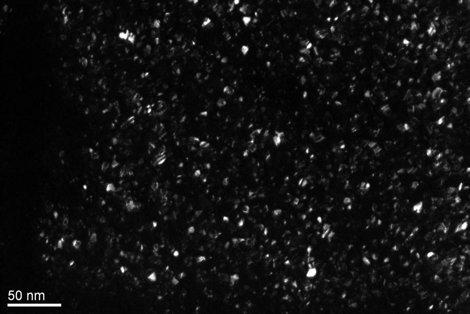
3 Nanocrystalline sample image/diffraction Bright field image setup - select direct beam with objective aperture Diffraction mode Image mode 5 Nanocrystalline sample image/diffraction Bright field image setup - select direct beam with objective aperture Diffraction mode Image mode Contrast from different crystals according to diffraction condition 5


4 Nanocrystalline sample image/diffraction Dark field image setup - select some transmitted beams with objective aperture Diffraction mode Image mode Only crystals diffracting strongly into objective aperture give bright contrast in image 6 Nanocrystalline sample image/diffraction Dark field image setup - select some transmitted beams with objective aperture Diffraction mode Image mode Only crystals diffracting strongly into objective aperture give bright contrast in image 7
 Short-range order produces diffuse rings in diffraction pattern Example: Figure from Williams & Carter Transmission Electron Microscopy Vitrified germanium (M. H. Bhat et al.")
5 Amorphous diffraction pattern Crystals: short-range order and long-range order Amorphous materials: no long-range order, but do have short-range order (roughly uniform interatomic distances as atoms pack around each other) Short-range order produces diffuse rings in diffraction pattern Example: Figure from Williams & Carter Transmission Electron Microscopy Vitrified germanium (M. H. Bhat et al. Nature (2007) 8 Diffraction contrast imaging of defects 9
6 Principle of diffraction contrast imaging Typically we use an objective aperture to select either the direct beam or a specific diffracted beam in the back-focal plane If the diffraction condition changes across the sample the intensity in the selected beam changes; the intensity in the image changes correspondingly In other words we make a spatial map of the intensity distribution across the sample in the selected beam: it is a mapping technique In this way we can image changes in crystal phase and structural defects such as dislocations As an example such TEM imaging was a key piece of evidence proving the existence of dislocations 10 2-beam diffraction and imaging Off-axis rays for DF image! aberrations and astigmatism! image moves when change objective lens focus Incident e-beam Specimen Objective lens BF DF Back focal plane First image plane 11

7 Scan coils/beam deflectors Can use deflectors in condenser lens system to shift beam (with no tilt) and to tilt beam (with no shift). Use incident beam tilt for centered dark field imaging. 12 Centred dark-field imaging Tilt incident! e-beam by 2!B Corresponds to tilting of Ewald sphere by 2"B, excite g h k l;! takes place of gh k l in SADP Specimen Objective lens Can now go from BF image to DF image by pressing button, no offaxis aberrations in DF image DF Back focal plane First image plane 13

8 Imaging crystal defects: dislocations Burgers vector for edge (top right) and screw (bottom right) dislocations 14 Imaging crystal defects: dislocations Local bending of crystal planes around the dislocation change their diffraction condition This produces a contrast in the image => g.b analysis for Burgers vector From Williams & Carter Transmission Electron Microscopy 15


+*+*',!\"#$%&%\"#'!\"#$%&%\"#( F )'*'*+,-)'*'*(*+, F F )'*'*+,-)'*'*+*+,./+*+*(00./'*'*+00.")
(*'*'*+,B*)'*'*(*+,B)'*(*'*+,* F F F F F F F F F F F F >%?6$*'@A)(*'*'*A,B)'*'*(*A,B)'*(*'*A, >%?")
9 Crystal defects: dislocations - g.b analysis On a simple level, planes parallel to the Burger s vector are not distorted by the dislocation! => these planes show no change in contrast a condition corresponding to g.b = 0 Invisibility criterion! u: dislocation line vector For edge dislocation, glide plane is parallel to b but can be buckled => still gives some contrast. Plane perpendicular to u and parallel to b gives no contrast 16 Crystal defects: dislocations - g.b analysis Example: analysis of threading dislocations of hexagonal GaN grown on sapphire substrate )+*+*',!"#$%&%"#'!"#$%&%"#( F )'*'*+,-)'*'*(*+, F F )'*'*+,-)'*'*+*+,./+*+*(00./'*'* %56 Images by! Emad Oveisi, CIME 12334%56 7%8%9:6;** 7%8%9:6;** F F F F F F F 1<56=*)+*+*+*',*2#$*1<56=)+*+*+*',* C$.6*'@A)(*'*'*+,B*)'*'*(*+,B)'*(*'*+,* F F F F F F F F F F F F >%?6$*'@A)(*'*'*A,B)'*'*(*A,B)'*(*'*A, >%?6$*'@A)(*'*'*A,B)'*'*(*A,B)'*(*'*A, D#E%8%9:6;** D#E%8%9:6;* F F F F F F C$.6*'@A)(*'*'*+,B*)'*'*(*+,B)'*(*'*+, F 1<56=*)+*+*+*',*2#$*1<56=)+*+*+*', 17

10 Convergent beam electron diffraction 18 Convergent beam electron diffraction Instead of parallel illumination with selected-area aperture, CBED uses! highly converged illumination to select a much smaller specimen region Small illuminated area =>! no thickness and orientation variations There is dynamical scattering, but it is useful! Can obtain disc and line patterns! packed with information: Figures by Jean-Paul Morniroli 19

11 Convergent beam electron diffraction Figures by Jean-Paul Morniroli 20 Convergent beam electron diffraction Figures by Jean-Paul Morniroli 21


12 Convergent beam electron diffraction Figures from Williams & Carter Transmission Electron Microscopy 22 Convergent beam electron diffraction Back-focal plane Image plane:! see image of focused e-beam Figures by Jean-Paul Morniroli 23


13 Convergent beam electron diffraction Exact 2- beam condition Back-focal plane Near 2- beam condition Image plane:! see image of focused e-beam 24 Excess and Deficient lines Look at Ewald sphere construction!here Ewald sphere intersects a HOLZ reflection exactly.! In this condition this HOLZ reflection must give 2#B scattering angle. If we draw in rays for excess and deficient lines at +#B and #B relative to the planes making the! reflection we see excess line intersects HOLZ reflection and deficient exactly. If we plot full angular range of incident beam it is clear that deficient HOLZ line crosses disc. k I k D


14 Excess and Deficient lines Look at Ewald sphere construction!here Ewald sphere intersects a HOLZ reflection exactly.! In this condition this HOLZ reflection must give 2#B scattering angle. If we draw in rays for excess and deficient lines at +#B and #B relative to the planes making the! reflection we see excess line intersects HOLZ reflection and deficient exactly. If we plot full angular range of incident beam it is clear that deficient HOLZ line crosses disc. k I k D Note: Excess and deficient lines! are often called Kikuchi lines HOLZ lines in CBED If HOLZ CBED discs at have excess lines at Bragg condition these give corresponding deficient lines crossing disc Figures by Jean-Paul Morniroli 27


15 HOLZ lines in CBED Because HOLZ lines contain 3D information, they also show true symmetry! e.g. three-fold {111} symmetry for cubic Al - unlike apparent six-fold axis in SADP or from ZOLZ Kikuchi lines Deficient lines for inclined planes: hu + kv + lw =? Fringes from 2D interactions/dynamical scattering; more thickness gives more fringes JEMS simulation for 300 nm thick Al, 200 kev beam energy 28 Thickness measurement by CBED Within CBED discs also obtain patterns from dynamical scattering. These patterns show fringes that are somewhat analogous to thickness fringes in the TEM image. Can measure thickness e.g. by comparing experimental data to simulation Example: Blochwave simulations for Al on [0 0 1] zone axis: 29
 =>")
 Example: Blochwave simulations for Al with (0 0 2) reflection excited: 31")
16 Thickness measurement by CBED Easier to think about in 2-beam Bragg scattering condition Different rays in the scattered beam sample different excitation errors for the reflection g Effectively we make a map of intensity for different excitation errors s along a chord in the disc g As thickness increases nodes in sinc 2 function move to smaller s (reciprocal relationship with thickness) => more fringes in the disc Intensity vs s for 2-beam condition, different specimen thicknesses t t = 10 nm t = 25 nm t = 50 nm 30 Thickness measurement by CBED Therefore to obtain CBED discs with 1-D fringes for thickness measurement tilt to 2-beam condition Possible to calculate thickness analytically (e.g. see Williams & Carter) Example: Blochwave simulations for Al with (0 0 2) reflection excited: 31


17 Identifying polarity in CBED Patterns from dynamical scattering in direct and diffraction discs allow determination of polarity of non-centrosymmetric crystals because dynamical scattering patterns are sensitive to channeling down particular atomic column JEMS simulation: GaN [ ] zone axis Simulation vs experiment: t = 100 nm t = 150 nm t = 200 nm t = 250 nm A. Brian Aebersold et al. Acta Materialia, Volume 130, 2017, ! 32 Zone axis CBED Instead of spot pattern, obtain disc pattern Larger convergence semi-angle " => larger discs Parallel beam SADP Si [001] " = 1.6 mrad " = 3.9 mrad 33


18 Zone axis CBED Instead of spot pattern, obtain disc pattern Larger convergence semi-angle α => larger discs α = 3.9 mrad α = 8.6 mrad α = 19.3 mrad See fringes in discs, and symmetry 34 Convergent beam electron diffraction practical example ZnO thin-film sample; Conditions: convergent beam, large condenser aperture, diffraction mode 35

19 Convergent beam electron diffraction practical example ZnO thin-film sample; Conditions: convergent beam, large condenser aperture, diffraction mode [1 1 0] zone axis 36 Kikuchi diffraction 37
20 Kikuchi lines Formation of bright and dark lines ( excess and deficient lines) by combination of incoherent scattering followed by elastic scattering in parallel incident beam geometry (e.g. SADP) The incoherent scattering (no preferential scattering vectors) is generally in forwards direction Cones of incoherently-scattered electrons then scattered by coherent elastic scattering, creating arcs in the diffraction plane. Because angles are small the arcs look straight. Resultant lines are very similar to the excess and deficient lines of CBED. They are equally sensitive to specimen orientation, and we use them e.g. to set a 2-beam condition. However the specimen must be thick (for sufficient inelastic scattering) and flat (to have sharp lines) to see them well. 38 Kikuchi line formation Treat problem in real space "B "B "B Treat 2-beam Bragg scattering condition "B "B Yellow volume represents intensity distribution of incoherent scattering event; mainly forward scattered h k l 2"B "B h k l origin of incoherent scattering event: h k l h k l 39
21 Treat problem in reciprocal space; Ewald sphere construction Forward scattering from incoherent scattering gives diffuse intensity at low scattering angles around Kikuchi line formation h k l "B "B ki Exact Bragg condition: Kikuchi lines coincide Deficient line: incoherent forwardscattered intensity removed from with Bragg spots Kikuchi line! dark line on brighter background kd ghkl h k l Excess line: incoherent forward-scattered intensity redistributed into Kikuchi line! bright line on low background 40 Kikuchi line formation Treat problem in real space Treat zone axis condition "B "B h k l "B "B h k l h k l h k l 41

22 Kikuchi line formation Treat problem in reciprocal space; Ewald sphere construction Remember Bragg spots only visible because of relrods and excitation error s Zone axis condition: (by geometry) Kikuchi lines halfway between Bragg spots ghkl h k l 2"B ki kd h k l Symmetrical relationship so both Kikuchi lines should have same intensity s ghkl 42 Kikuchi diffraction Figures by Jean-Paul Morniroli Position of the Kikuchi line pairs of (excess and deficient) very sensitive to specimen orientation Can use to identify excitation vector; in particular s = 0 when diffracted beam coincides! exactly with excess Kikuchi line (and direct beam with deficient Kikuchi line) Quiz: what happens to width of Kikuchi line pairs as (h k l) indices become bigger?! Answer: larger indices (h k l)! greater scattering angle "B! larger width of line pairs 43


![Si [2 2 3] Obviously Kikuchi lines can be useful, but can be hard to see (e.g.](/docs-images/76/73061910/images/23-2.jpg "from insufficient thickness, diffuse lines from crystal bending, strain).")
23 Kikuchi lines road map to reciprocal space Kikuchi lines traverse reciprocal space, converging on zone axes - use them to navigate reciprocal space as you tilt the specimen! Examples: Si simulations using JEMS Si [1 1 0] Si [1 1 0] tilted off zone axis Si [2 2 3] Obviously Kikuchi lines can be useful, but can be hard to see (e.g. from insufficient thickness, diffuse lines from crystal bending, strain). Need an alternative method Mapping in nano-beam diffraction mode 45


24 Nano-beam set-up In nano-beam mode, use small C2 condenser aperture and excited 3rd condenser lens (e.g. condenser mini-lens) to make near-parallel beam of 2 3 nm diameter on specimen surface Typical convergence semi-angle alpha ~0.5 1 mrad; therefore obtain spot-like diffraction patterns from very small probe 46 Orientation image mapping in TEM The NanoMEGAS ASTAR system scans the nanobeam across sample while recording diffraction patterns to make a map with one diffraction pattern for every pixel positions x, y Template matching then used to identify phase and orientation; each pattern correlated with 100s-1000s of patterns simulated at different orientations and for different phases Much higher spatial resolution than EBSD in SEM, and angular resolution of 1 Can combine with precession for greater reliability of indexing [1] E.F. Rauch et al., Micros. Anal. Nanotech. Supplement, 22(6), S5-S8,


25 ASTAR example: nanocrystalline ZnO Plan-view sample of textured, nanocrystalline ZnO thin-film 750 x 750 pixel map, 2 3 nm probe size, 2 nm step size {10-10} Y Z X {0001} {2-1-10} A. Brian Aebersold, CIME 48 Imaging and diffraction examples summary Diffraction useful for measuring orientation relationships and polycrystalline crystal structures For correct dark-field imaging we tilt incident beam to do centred dark-field imaging free of aberrations from displacing the objective aperture Can use centred dark-field e.g. for analysing dislocations Parallel beam diffraction can also give excess and deficient lines via incoherent followed by coherent scattering: Kikuchi diffraction Automated crystal orientation and phase mapping is also now possible and can give high quality data on nanocrystalline materials nature Convergent beam electron diffraction is a powerful technique allowing to see excess and deficient lines which are very sensitive to specimen orientation, and dynamical scattering patterns that inform e.g. on sample thickness and polarity 49
26 Resources Transmission Electron Microscopy by Williams and Carter Large Angle Convervent Beam Electron Diffraction, Jean-Paul Morniroli JEMS Pierre Stadelmann s electron microscopy simulation software: Open access database of.cif files: 50
TEM imaging and diffraction examples
 TEM imaging and diffraction examples Duncan Alexander EPFL-CIME 1 Diffraction examples Kikuchi diffraction Epitaxial relationships Polycrystalline samples Amorphous materials Contents Convergent beam electron
Diffraction Going further
 Diffraction Going further Duncan Alexander! EPFL-CIME 1 Contents Higher order Laue zones (HOLZ)! Kikuchi diffraction! Convergent beam electron diffraction (CBED)! HOLZ lines in CBED! Thickness measurements!
Electron Microscopy. Dynamical scattering
 Electron Microscopy 4. TEM Basics: interactions, basic modes, sample preparation, Diffraction: elastic scattering theory, reciprocal space, diffraction pattern, Laue zones Diffraction phenomena Image formation:
Imaging with Diffraction Contrast
 Imaging with Diffraction Contrast Duncan Alexander EPFL-CIME 1 Introduction When you study crystalline samples TEM image contrast is dominated by diffraction contrast. An objective aperture to select either
Dynamical Scattering and Defect Imaging
 Dynamical Scatterin and Defect Imain Duncan Alexander! EPFL-CIME 1 Contents Dynamical scatterin! Thickness frines! Double diffraction! Defect imain! 2-beam (stron beam) set-up!.b dislocation analysis!
TEM and Electron Diffraction Keith Leonard, PhD (1999) U. Cincinnati
 U. Cincinnati") TEM and Electron Diffraction Keith Leonard, PhD (1999) U. Cincinnati Electron Microscopes: Electron microscopes, such as the scanning electron microscope (SEM) and transmission electron microscope (TEM)
TEM and Electron Diffraction Keith Leonard, PhD (1999) U. Cincinnati Electron Microscopes: Electron microscopes, such as the scanning electron microscope (SEM) and transmission electron microscope (TEM)
Principles & Practice of Electron Diffraction
 Principles & Practice of Electron Diffraction Duncan Alexander EPFL-CIME 1 Contents Introduction to electron diffraction Elastic scattering theory Basic crystallography & symmetry Electron diffraction
Signals from a thin sample
 Signals from a thin sample Auger electrons Backscattered electrons BSE Incident beam secondary electrons SE Characteristic X-rays visible light 1-100 nm absorbed electrons Specimen electron-hole pairs
EMSE Weak-Beam Dark-Field Technique
 Weak-Beam Dark-Field Technique 1 Weak-Beam Dark-Field Imaging Basic Idea recall bright-field contrast of dislocations: specimen close to Bragg condition, s î 0 near the dislocation core, some planes curved
11.3 The analysis of electron diffraction patterns
 11.3 The analysis of electron diffraction patterns 277 diameter) Ewald reflecting sphere, the extension of the reciprocal lattice nodes and the slight buckling of the thin foil specimens all of which serve
Microstructural Characterization of Materials
 Microstructural Characterization of Materials 2nd Edition DAVID BRANDON AND WAYNE D. KAPLAN Technion, Israel Institute of Technology, Israel John Wiley & Sons, Ltd Contents Preface to the Second Edition
Crystallographic Textures Measurement
 Crystallographic Textures Measurement D. V. Subramanya Sarma Department of Metallurgical and Materials Engineering Indian Institute of Technology Madras E-mail: vsarma@iitm.ac.in Macrotexture through pole
CHEM-E5225 :Electron Microscopy Imaging II
 CHEM-E5225 :Electron Microscopy Imaging II D.B. Williams, C.B. Carter, Transmission Electron Microscopy: A Textbook for Materials Science, Springer Science & Business Media, 2009. Z. Luo, A Practical Guide
Kinematical theory of contrast
 Kinematical theory of contrast Image interpretation in the EM the known distribution of the direct and/or diffracted beam on the lower surface of the crystal The image on the screen of an EM = the enlarged
STUDY & ANALYSIS OF ALUMINIUM FOIL AND ANATASE TITANIUM OXIDE (TiO2) USING TRANSMISSION ELECTRON MICROSCOPY
 USING TRANSMISSION ELECTRON MICROSCOPY") STUDY & ANALYSIS OF ALUMINIUM FOIL AND ANATASE TITANIUM OXIDE (TiO2) USING TRANSMISSION ELECTRON MICROSCOPY Ayush Garg Department of Chemical and Materials Engineering, University of Auckland, Auckland,
STUDY & ANALYSIS OF ALUMINIUM FOIL AND ANATASE TITANIUM OXIDE (TiO2) USING TRANSMISSION ELECTRON MICROSCOPY Ayush Garg Department of Chemical and Materials Engineering, University of Auckland, Auckland,
Practical 2P8 Transmission Electron Microscopy
 Practical 2P8 Transmission Electron Microscopy Originators: Dr. M. L. Jenkins and Prof. J. M. Titchmarsh What you should learn from this practical Science This practical ties-in with the lecture course
Practical 2P8 Transmission Electron Microscopy
 Practical 2P8 Transmission Electron Microscopy Originators: Dr. N.P. Young and Prof. J. M. Titchmarsh What you should learn from this practical Science This practical ties-in with the lecture course on
Fundamentals of X-ray diffraction and scattering
 Fundamentals of X-ray diffraction and scattering Don Savage dsavage@wisc.edu 1231 Engineering Research Building (608) 263-0831 X-ray diffraction and X-ray scattering Involves the elastic scattering of
TEM Study of the Morphology Of GaN/SiC (0001) Grown at Various Temperatures by MBE
 Grown at Various Temperatures by MBE") TEM Study of the Morphology Of GaN/SiC (0001) Grown at Various Temperatures by MBE W.L. Sarney 1, L. Salamanca-Riba 1, V. Ramachandran 2, R.M Feenstra 2, D.W. Greve 3 1 Dept. of Materials & Nuclear Engineering,
TEM Study of the Morphology Of GaN/SiC (0001) Grown at Various Temperatures by MBE W.L. Sarney 1, L. Salamanca-Riba 1, V. Ramachandran 2, R.M Feenstra 2, D.W. Greve 3 1 Dept. of Materials & Nuclear Engineering,
Electron microscopy II
 Electron microscopy II Nanomaterials characterization I RNDr. Věra Vodičková, PhD. Interaction ction: electrons solid matter Signal types SE.secondary e - AE Auger s e - BSE back scattered e - X-ray photons,
Dislocations Linear Defects
 Dislocations Linear Defects Dislocations are abrupt changes in the regular ordering of atoms, along a line (dislocation line) in the solid. They occur in high density and are very important in mechanical
Transmission Electron Microscopy (TEM) Prof.Dr.Figen KAYA
 Prof.Dr.Figen KAYA") Transmission Electron Microscopy (TEM) Prof.Dr.Figen KAYA Transmission Electron Microscope A transmission electron microscope, similar to a transmission light microscope, has the following components along
Transmission Electron Microscopy (TEM) Prof.Dr.Figen KAYA Transmission Electron Microscope A transmission electron microscope, similar to a transmission light microscope, has the following components along
Transmission Kikuchi Diffraction in the Scanning Electron Microscope
 Transmission Kikuchi Diffraction in the Scanning Electron Microscope Robert Keller, Roy Geiss, Katherine Rice National Institute of Standards and Technology Nanoscale Reliability Group Boulder, Colorado
Supplementary Materials for
 advances.sciencemag.org/cgi/content/full/4/8/eaat4712/dc1 Supplementary Materials for In situ manipulation and switching of dislocations in bilayer graphene Peter Schweizer, Christian Dolle, Erdmann Spiecker*
Electron channelling contrast imaging (ECCI) an amazing tool for observations of crystal lattice defects in bulk samples
 an amazing tool for observations of crystal lattice defects in bulk samples") Electron channelling contrast imaging (ECCI) an amazing tool for observations of crystal lattice defects in bulk samples Stefan Zaefferer with contributions of N. Elhami, (general & steels) Z. Li F. Ram,
Electron channelling contrast imaging (ECCI) an amazing tool for observations of crystal lattice defects in bulk samples Stefan Zaefferer with contributions of N. Elhami, (general & steels) Z. Li F. Ram,
INTERPRETATION OF TRANSMISSION ELECTRON MICROGRAPHS
 3 INTERPRETATION OF TRANSMISSION ELECTRON MICROGRAPHS Already published in this series 1. The Operation and Calibration of the Electron Microscope 2. Electron Diffraction in the Electron Microscope In
Transmission Electron Microscopy. J.G. Wen, C.H. Lei, M. Marshall W. Swiech, J. Mabon, I. Petrov
 Advanced Materials Characterization Workshop Transmission Electron Microscopy J.G. Wen, C.H. Lei, M. Marshall W. Swiech, J. Mabon, I. Petrov Supported by the U.S. Department of Energy under grants DEFG02-07-ER46453
The object of this experiment is to test the de Broglie relationship for matter waves,
 Experiment #58 Electron Diffraction References Most first year texts discuss optical diffraction from gratings, Bragg s law for x-rays and electrons and the de Broglie relation. There are many appropriate
Defect and chemical analysis in the TEM
 THE UNIVERSITY Defect and chemical analysis in the TEM Defect and chemical analysis in the TEM I.P. Jones. Chemical analysis: EDX. Chemical analysis: PEELS Centre for Electron Microscopy OF BIRMINGHAM
On-axis Transmission Kikuchi Diffraction in the SEM. Performances and Applications
 On-axis Transmission Kikuchi Diffraction in the SEM. Performances and Applications Etienne Brodu, Emmanuel Bouzy, Jean-Jacques Fundenberger Séminaire «les microscopies électroniques à Metz et à Nancy»
EBSD Basics EBSD. Marco Cantoni 021/ Centre Interdisciplinaire de Microscopie Electronique CIME. Phosphor Screen. Pole piece.
 EBSD Marco Cantoni 021/693.48.16 Centre Interdisciplinaire de Microscopie Electronique CIME EBSD Basics Quantitative, general microstructural characterization in the SEM Orientation measurements, phase
UNIVERSITY OF OSLO. Faculty of Mathematics and Natural Sciences
 Page 1 UNIVERSITY OF OSLO Faculty of Mathematics and Natural Sciences Exam in MENA3100 Characterization of materials Day of exam: 12th. June 2015 Exam hours: 14:30 This examination paper consists of 5
X-RAY DIFFRACTION IN SEMICONDUCTOR INDUSTRY AND RESEARCH
 X-RAY DIFFRACTION IN SEMICONDUCTOR INDUSTRY AND RESEARCH M. Leszczyński High Pressure Research Center UNIPRESS, Sokolowska 29/37, 01 142 Warsaw, Poland, e-mail: mike@unipress.waw.pl ABSTRACT The paper
Conventional TEM. N o r t h w e s t e r n U n i v e r s i t y - M a t e r i a l s S c i e n c e
 Conventional TEM STEM N o r t h w e s t e r n U n i v e r s i t y - M a t e r i a l s S c i e n c e Reciprocity 1 1 C CCCCCCCC(2ππππππ. rr) CCCCCC(2ππππππ. rr) Reciprocity 2 1 C+D CC(gg)CCCCCC(2ππππππ.
Thin Film Scattering: Epitaxial Layers
 Thin Film Scattering: Epitaxial Layers 6th Annual SSRL Workshop on Synchrotron X-ray Scattering Techniques in Materials and Environmental Sciences: Theory and Application May 29-31, 2012 Thin films. Epitaxial
Structural Features of = 3 and 9, [110] GaAs Tilt Grain Boundaries
![Structural Features of = 3 and 9, [110] GaAs Tilt Grain Boundaries](/thumbs/86/93976988.jpg "Structural Features of = 3 and 9, [110] GaAs Tilt Grain Boundaries") Jpn. J. Appl. Phys. Vol. 40 (2001) pp. 4458 4465 Part 1, No. 7, July 2001 c 2001 The Japan Society of Applied Physics Structural Features of = 3 and 9, [110] GaAs Tilt Grain Boundaries Nam-Hee CHO and
Jpn. J. Appl. Phys. Vol. 40 (2001) pp. 4458 4465 Part 1, No. 7, July 2001 c 2001 The Japan Society of Applied Physics Structural Features of = 3 and 9, [110] GaAs Tilt Grain Boundaries Nam-Hee CHO and
Chapter 3 Basic Crystallography and Electron Diffraction from Crystals. Lecture 9. Chapter 3 CHEM Fall, L. Ma
 Chapter 3 Basic Crystallography and Electron Diffraction from Crystals Lecture 9 Outline The geometry of electron diffraction Crystallography Kinetic Theory of Electron diffraction Diffraction from crystals
High-resolution electron microscopy of grain boundary structures in yttria-stabilized cubic zirconia
 Mat. Res. Soc. Symp. Proc. Vol. 654 2001 Materials Research Society High-resolution electron microscopy of grain boundary structures in yttria-stabilized cubic zirconia K. L. Merkle, L. J. Thompson, G.-R.
Why does the growth rate slow down as a precipitate thickens during diffusion-controlled growth?
 Part II: Worked Examples H. K. D. H. Bhadeshia Question 14 Why does the growth rate slow down as a precipitate thickens during diffusion-controlled growth? The surface of a metal can be nitrided to form
Searching for new API Polymorphs Crystal Structure Determination of Pharmaceutical crystals using Electron Diffraction Tomography
 Searching for new API Polymorphs Crystal Structure Determination of Pharmaceutical crystals using Electron Diffraction Tomography Dr. Partha Pratim Das Application Specialist NanoMEGAS SPRL, Belgium This
Carnegie Mellon MRSEC
 Carnegie Mellon MRSEC Texture, Microstructure & Anisotropy, Fall 2009 A.D. Rollett, P. Kalu 1 ELECTRONS SEM-based TEM-based Koseel ECP EBSD SADP Kikuchi Different types of microtexture techniques for obtaining
Supplementary Material
 Supplementary Material Self-patterning Gd nano-fibers in Mg-Gd alloys Yangxin Li 1,2, Jian Wang 3, Kaiguo Chen 4, Meiyue Shao 2, Yao Shen 1 *, Li Jin 2 *, Guozhen Zhu 1 * 1 State Key Laboratory of Metal
Structure factors and crystal stacking
 Structure factors and crystal stacking Duncan Alexander EPFL-CIME 1 Contents Atomic scattering theory Crystal structure factors Close packed structures Systematic absences Twinning and stacking faults
This lecture is part of the Basic XRD Course.
 This lecture is part of the Basic XRD Course. Basic XRD Course 1 A perfect polycrystalline sample should contain a large number of crystallites. Ideally, we should always be able to find a set of crystallites
Twins & Dislocations in HCP Textbook & Paper Reviews. Cindy Smith
 Twins & Dislocations in HCP Textbook & Paper Reviews Cindy Smith Motivation Review: Outline Crystal lattices (fcc, bcc, hcp) Fcc vs. hcp stacking sequences Cubic {hkl} naming Hcp {hkil} naming Twinning
Strain. Two types of stresses: Usually:
 Stress and Texture Strain Two types of stresses: microstresses vary from one grain to another on a microscopic scale. macrostresses stress is uniform over large distances. Usually: macrostrain is uniform
Diffraction Basics. The qualitative basics:
 The qualitative basics: Diffraction Basics Coherent scattering around atomic scattering centers occurs when x-rays interact with material In materials with a crystalline structure, x-rays scattered in
High Resolution X-ray Diffraction
 High Resolution X-ray Diffraction Nina Heinig with data from Dr. Zhihao Donovan Chen, Panalytical and slides from Colorado State University Outline Watlab s new tool: Panalytical MRD system Techniques:
SECTION A. NATURAL SCIENCES TRIPOS Part IA. Friday 4 June to 4.30 MATERIALS AND MINERAL SCIENCES
 NATURAL SCIENCES TRIPOS Part IA Friday 4 June 1999 1.30 to 4.30 MATERIALS AND MINERAL SCIENCES Answer five questions; two from each of sections A and B and one from section C. Begin each answer at the
EBSD Electron BackScatter Diffraction Principle and Applications
 EBSD Electron BackScatter Diffraction Principle and Applications Dr. Emmanuelle Boehm-Courjault EPFL STI IMX Laboratoire de Simulation des Matériaux LSMX emmanuelle.boehm@epfl.ch 1 Outline! Introduction!
3. Anisotropic blurring by dislocations
 Dynamical Simulation of EBSD Patterns of Imperfect Crystals 1 G. Nolze 1, A. Winkelmann 2 1 Federal Institute for Materials Research and Testing (BAM), Berlin, Germany 2 Max-Planck- Institute of Microstructure
Observation in the GB (Gentle Beam) Capabilities
 Capabilities") A field-emission cathode in the electron gun of a scanning electron microscope provides narrower probing beams at low as well as high electron energy, resulting in both improved spatial resolution and
A field-emission cathode in the electron gun of a scanning electron microscope provides narrower probing beams at low as well as high electron energy, resulting in both improved spatial resolution and
JECP/HOLZ, an Interactive Computer Program for Simulation of HOLZ Pattern
 JECP/HOLZ, an Interactive Computer Program for Simulation of HOLZ Pattern (Version 2t) X.Z. Li, Ph. D Copyright(C) 2002-2017 LANDYNE All Rights Reserved. Contents: 1. Purpose of the program 2. Graphic
LECTURE 7. Dr. Teresa D. Golden University of North Texas Department of Chemistry
 LECTURE 7 Dr. Teresa D. Golden University of North Texas Department of Chemistry Diffraction Methods Powder Method For powders, the crystal is reduced to a very fine powder or microscopic grains. The sample,
CRYSTAL STRUCTURE DETERMINATION OF PHARMACEUTICALS WITH ELECTRON DIFFRACTION
 CRYSTAL STRUCTURE DETERMINATION OF PHARMACEUTICALS WITH ELECTRON DIFFRACTION Dr. Partha Pratim Das Application Specialist, NanoMEGAS SPRL, Belgium pharma@nanomegas.com www.nanomegas.com This document was
X-RAY DIFFRACTIO N B. E. WARREN
 X-RAY DIFFRACTIO N B. E. WARREN Chapter 1 X-Ray Scattering by Atom s 1.1 Classical scattering by a free electron 1 1.2 Polarization by scattering 4 1.3 Scattering from several centers, complex representation
Single crystal X-ray diffraction. Zsolt Kovács
 Single crystal X-ray diffraction Zsolt Kovács based on the Hungarian version of the Laue lab description which was written by Levente Balogh, Jenő Gubicza and Lehel Zsoldos INTRODUCTION X-ray diffraction
Supporting Information
 Supporting Information Dynamics and Removal Pathway of Edge Dislocations in Imperfectly Attached PbTe Nanocrystal Pairs; Towards Design Rules for Oriented Attachment Justin C. Ondry,, Matthew R. Hauwiller,,
Thin Film Scattering: Epitaxial Layers
 Thin Film Scattering: Epitaxial Layers Arturas Vailionis First Annual SSRL Workshop on Synchrotron X-ray Scattering Techniques in Materials and Environmental Sciences: Theory and Application Tuesday, May
Introduction to Electron Backscattered Diffraction. TEQIP Workshop HREXRD Feb 1 st to Feb 5 th 2016
 Introduction to Electron Backscattered Diffraction 1 TEQIP Workshop HREXRD Feb 1 st to Feb 5 th 2016 SE vs BSE 2 Ranges and interaction volumes 3 (1-2 m) http://www4.nau.edu/microanalysis/microprobe/interact-effects.html
Supplementary Figure 1: Geometry of the in situ tensile substrate. The dotted rectangle indicates the location where the TEM sample was placed.
 Supplementary Figures Supplementary Figure 1: Geometry of the in situ tensile substrate. The dotted rectangle indicates the location where the TEM sample was placed. Supplementary Figure 2: The original
Precision Without Compromise
 D1 EVOLUTION Precision Without Compromise Versatile and user-friendly high resolution and multipurpose X-ray diffractometer for the characterization of advanced materials www.jvsemi.com D1 Overview Introduction
Materials Characterization for Stress Management
 Materials Characterization for Stress Management Ehrenfried Zschech, Fraunhofer IZFP Dresden, Germany Workshop on Stress Management for 3D ICs using TSVs San Francisco/CA, July 13, 2010 Outline Stress
Application of Scanning Electron Microscope to Dislocation Imaging in Steel
 Application of Scanning Electron Microscope to Dislocation Imaging in Steel Masaaki Sugiyama and Masateru Shibata Advanced Technology Research Laboratories, Nippon Steel Corporation SM Business Unit, JEOL
Fundamentals of Crystalline State p. 1 Introduction p. 1 Crystalline state p. 2 Crystal lattice and crystal structure p. 4 Shape of the unit cell p.
 Preface p. xvii Fundamentals of Crystalline State p. 1 Introduction p. 1 Crystalline state p. 2 Crystal lattice and crystal structure p. 4 Shape of the unit cell p. 6 Content of the unit cell p. 7 Asymmetric
Application of ASTAR/precession electron diffraction technique to quantitatively study defects in nanocrystalline metallic materials
 Graduate Theses and Dissertations Iowa State University Capstones, Theses and Dissertations 2017 Application of ASTAR/precession electron diffraction technique to quantitatively study defects in nanocrystalline
Relation between Microstructure and 2DEG Properties of AlGaN/GaN Structures
 2. Experimental The AlGaN/GaN structures have been grown by low-pressure metalorganic vapor phase epitaxy (LP-MOVPE) on c-plane sapphire substrates [2], using ammonia, TMGa and TMAl as precursors. After
Supporting Information. Solution-Processed 2D PbS Nanoplates with Residual Cu 2 S. Exhibiting Low Resistivity and High Infrared Responsivity
 Supporting Information Solution-Processed 2D PbS Nanoplates with Residual Cu 2 S Exhibiting Low Resistivity and High Infrared Responsivity Wen-Ya Wu, Sabyasachi Chakrabortty, Asim Guchhait, Gloria Yan
Fundamentals of Crystalline State and Crystal Lattice p. 1 Crystalline State p. 2 Crystal Lattice and Unit Cell p. 4 Shape of the Unit Cell p.
 Fundamentals of Crystalline State and Crystal Lattice p. 1 Crystalline State p. 2 Crystal Lattice and Unit Cell p. 4 Shape of the Unit Cell p. 7 Crystallographic Planes, Directions, and Indices p. 8 Crystallographic
JSM-7800F Field Emission Scanning Electron Microscope
 JSM-7800F catalogue JSM-7800F Field Emission Scanning Electron Microscope We provide high performance The Ultimate Research Tool for Multi-Disciplinary Research Institutions Extreme resolution The super
COMPARISON OF TEXTURE IN COPPER AND ALUMINUM THIN FILMS DETERMINED BY XRD AND EBSD *
 COMPARISON OF TEXTURE IN COPPER AND ALUMINUM THIN FILMS DETERMINED BY XRD AND EBSD * 201 J. Müller 1, D. Balzar 1,2, R.H. Geiss 1, D.T. Read 1, and R.R. Keller 1 1 Materials Reliability Division, National
The principles and practice of electron microscopy
 The principles and practice of electron microscopy Second Edition Ian M. Watt CAMBRIDGE UNIVERSITY PRESS Contents Preface tofirstedition page ix Preface to second edition xi 1 Microscopy with light and
The application of scanning electron beam anomalous transmission patterns in mineralogy
 MINERALOGICAL MAGAZINE, JUNE 1969, VOL. 37, NO. 286 The application of scanning electron beam anomalous transmission patterns in mineralogy M. P. JONES, B.SC., D.I.C., A.M.I.M.M., AND J. GAVRILOVIC, PH.D.,
SI GUIDE. File Name: Supplementary Information Description: Supplementary Figures, Supplementary Notes and Supplementary References.
 SI GUIDE File Name: Supplementary Information Description: Supplementary Figures, Supplementary Notes and Supplementary References. File Name: Supplementary Movie 1 Description: (the movie from which Figs.
TRANSMISSION ELECTRON MICROSCOPY OF OPTOELECTRONIC MATERIALS BASICS AND ADVANCED TECHNIQUES
 TRANSMISSION ELECTRON MICROSCOPY OF OPTOELECTRONIC MATERIALS BASICS AND ADVANCED TECHNIQUES Fritz Phillipp Max-Planck-Institut für Metallforschung, Heisenbergstr. 3, D-70569 Stuttgart, Germany ABSTRACT
Contents 1. of a higher level of mathematics, physics, or crystallography.
 Contents 1 1 Diffraction and the X-Ray Powder Diffractometer... 1 1.1 Diffraction... 1 1.1.1 Introduction to Diffraction... 1 1.1.2 Bragg s Law... 3 1.1.3 StrainEffects... 6 1.1.4 SizeEffects... 6 1.1.5
FePd (216 Å) grown on (001) MgO. 2θ(deg)
 grown on (001) MgO. 2θ(deg)") Major Findings 1. FePd thin films The structural characterization of the films grown at various substrate temperatures (RT- 700 o C) was performed ex-situ using X-Ray Diffraction (XRD). The optimum substrate
Major Findings 1. FePd thin films The structural characterization of the films grown at various substrate temperatures (RT- 700 o C) was performed ex-situ using X-Ray Diffraction (XRD). The optimum substrate
Answer All Questions. All Questions Carry Equal Marks. Time: 20 Min. Marks: 10.
 Code No: 09A1BS02 Set No. 1 JAWAHARLAL NEHRU TECHNOLOGICAL UNIVERSITY HYDERABAD I B.Tech. I Mid Examinations, November 2009 ENGINEERING PHYSICS Objective Exam Name: Hall Ticket No. A Answer All Questions.
A Quantitative Evaluation of Microstructure by Electron Back-Scattered Diffraction Pattern Quality Variations
 Microsc. Microanal. 19, S5, 83 88, 2013 doi:10.1017/s1431927613012397 A Quantitative Evaluation of Microstructure by Electron Back-Scattered Diffraction Pattern Quality Variations SukHoonKang, 1 Hyung-Ha
Electron microscopy s multi-tool: the Scanning Transmission Electron Microscope. Advanced Technology Institute, University of Surrey, Guildford, UK.
 Electron microscopy s multi-tool: the Scanning Transmission Electron Microscope Vlad Stolojan Advanced Technology Institute, University of Surrey, Guildford, UK. Biography: Vlad Stolojan obtained his BSc
Structures of AlN/VN superlattices with different AlN layer thicknesses
 Structures of AlN/VN superlattices with different AlN layer thicknesses Quan Li a) Department of Physics, The Chinese University of Hong Kong, Shatin, New Territory, Hong Kong I.W. Kim, S.A. Barnett, and
9/28/2013 9:26 PM. Chapter 3. The structure of crystalline solids. Dr. Mohammad Abuhaiba, PE
 Chapter 3 The structure of crystalline solids 1 2 Why study the structure of crystalline solids? Properties of some materials are directly related to their crystal structure. Significant property differences
Building An Ultrafast Photon-Induced Near-field Transmission Electron Microscope
 Building An Ultrafast Photon-Induced Near-field Transmission Electron Microscope Dr. Tom T.A. Lummen École Polytechnique Fédérale de Lausanne -- LUMES Photonic Instruments 2013 September 11, 2013 Zürich,
ECCI of AlGaN/GaN HEMT structures grown on Si
 ECCI of AlGaN/GaN HEMT structures grown on Si D. Thomson 1, G. Naresh-Kumar 1, B. Hourahine 1, C. Trager-Cowan 1, P. Wright 2 and T. Martin 2 1 Dept. Of Physics, SUPA, University of Strathclyde, Glasgow
Heterostructures of Oxides and Semiconductors - Growth and Structural Studies
 Heterostructures of Oxides and Semiconductors - Growth and Structural Studies Beamline 17B1 W20 X-ray Scattering beamline Authors M. Hong and J. R. Kwo National Tsing Hua University, Hsinchu, Taiwan H.
Workshop RIETVELD REFINEMENT OF DIFFRACTION PATTERNS Program Monday June 1st, Introduction to Rietveld refinement S.
 Workshop RIETVELD REFINEMENT OF DIFFRACTION PATTERNS Program Monday June 1st, 2009 9.00 13.00 Introduction to Rietveld refinement S.Enzo Università di Sassari X-ray diffraction for bulk samples and thin
Rietveld analysis of policrystalline materials using precession of electron diffraction
 Romanian Biotechnological Letters Copyright 2010 University of Bucharest Vol. 15, No.3, 2010, Supplement Printed in Romania. All rights reserved ORIGINAL PAPER Rietveld analysis of policrystalline materials
X-Ray Diffraction. Nicola Pinna
 X-Ray Diffraction Nicola Pinna Department of Chemistry, CICECO, University of Aveiro, 3810-193 Aveiro, Portugal. School of Chemical and Biological Engineering, College of Engineering, Seoul National University
Index. Cambridge University Press Introduction to Elasticity Theory for Crystal Defects R. W. Balluffi. Index.
 Airy stress functions formulation of 60 1 table of 426 alternator operator 419 Brown s formula 255 Burgers equation 264 5 Christoffel stiffness tensor 34 corresponding elastic fields 25 7 curvature tensor,
Introduction to XRD analysis of modern functional thin films using a 2-dimensional detector (2) Analysis of epitaxial films
 Analysis of epitaxial films") Technical articles Introduction to XRD analysis of modern functional thin films using a 2-dimensional detector (2) Analysis of epitaxial films Katsuhiko Inaba* 1. Introduction Epitaxial thin films are
Technical articles Introduction to XRD analysis of modern functional thin films using a 2-dimensional detector (2) Analysis of epitaxial films Katsuhiko Inaba* 1. Introduction Epitaxial thin films are
In Situ Observation of Dislocation Nucleation and Escape in a Submicron Al Single Crystal
 Supplementary Information for In Situ Observation of Dislocation Nucleation and Escape in a Submicron Al Single Crystal Sang Ho Oh*, Marc Legros, Daniel Kiener and Gerhard Dehm *To whom correspondence
What if your diffractometer aligned itself?
 Ultima IV Perhaps the greatest challenge facing X-ray diffractometer users today is how to minimize time and effort spent on reconfiguring of the system for different applications. Wade Adams, Ph.D., Director,
SiC crystal growth from vapor
 SiC crystal growth from vapor Because SiC dissolves in Si and other metals can be grown from melt-solutions: Liquid phase epitaxy (LPE) Solubility of C in liquid Si is 0.029% at 1700oC high T process;
Advances in EBSD Analysis Using Novel Dynamical Pattern Simulation Software
 Advances in EBSD Analysis Using Novel Dynamical Pattern Simulation Software Bruker Nano GmbH, Berlin Webinar, November 5 th, 2014 Innovation with Integrity Presenters Dr. Daniel Goran Product Manager EBSD,
Chemically Tunable Full Spectrum Optical Properties of 2D Silicon Telluride Nanoplates
 SUPPORTING INFORMATION Chemically Tunable Full Spectrum Optical Properties of 2D Silicon Telluride Nanoplates Mengjing Wang,, Gabriella Lahti, David Williams, and Kristie J. Koski * Department of Chemistry,
Structure Analysis of -phase in Sb-Te Alloys by HRTEM* 1
 Materials Transactions, Vol. 45, No. 8 (2004) pp. 2673 to 2677 #2004 The Japan Institute of Metals Structure Analysis of -phase in Sb-Te Alloys by HRTEM* 1 Yoshiyuki Nakata 1, Takehito Suenaga 1; * 2,
The growth of patterned ceramic thin films from polymer precursor solutions Göbel, Ole
 University of Groningen The growth of patterned ceramic thin films from polymer precursor solutions Göbel, Ole IMPORTANT NOTE: You are advised to consult the publisher's version (publisher's PDF) if you
CURVATURE MEASUREMENTS OF STRESSED SURFACE-ACOUSTIC- WAVE FILTERS USING BRAGG ANGLE CONTOUR MAPPING
 86 CURVATURE MEASUREMENTS OF STRESSED SURFACE-ACOUSTIC- WAVE FILTERS USING BRAGG ANGLE CONTOUR MAPPING ABSTRACT Paul M. Adams The Aerospace Corporation Los Angeles, CA 90009 Surface-acoustic-wave (SAW)
AP 5301/8301 Instrumental Methods of Analysis and Laboratory Lecture 4 Microscopy (III): Transmission Electron Microscopy (TEM)
: Transmission Electron Microscopy (TEM)") 1 AP 5301/8301 Instrumental Methods of Analysis and Laboratory Lecture 4 Microscopy (III): Transmission Electron Microscopy (TEM) Prof YU Kin Man E-mail: kinmanyu@cityu.edu.hk Tel: 3442-7813 Office: P6422
1 AP 5301/8301 Instrumental Methods of Analysis and Laboratory Lecture 4 Microscopy (III): Transmission Electron Microscopy (TEM) Prof YU Kin Man E-mail: kinmanyu@cityu.edu.hk Tel: 3442-7813 Office: P6422
Philips Analytical, Lelyweg 1, 7602 EA Almelo, The Netherlands
 Copyright(c)JCPDS-International Centre for Diffraction Data 2001,Advances in X-ray Analysis,Vol.44 284 MICRO-DIFFRACTION WITH MONO-CAPILLARIES M.J. Fransen, J.H.A. Vasterink and J. te Nijenhuis Philips