microdice System for Separation of SiC Wafer Using Thermal Laser Separation
|
|
|
- Drusilla Reed
- 6 years ago
- Views:
Transcription

1 microdice System for Separation of SiC Wafer Using Thermal Laser Separation - System Integration Technologies Fraunhofer ENAS - (Ronny Neubert, 3D-Micromac AG)


2 3D-Micromac At a Glance Manufacturer and service provider for Laser micromachining systems and Production equipment for printing and coating technologies Design of complete machining systems including process development and service in-house Founded in 2002 Founded US subsidiary in 2014
3 1. Thermal Laser Separation (TLS-Dicing ) 2. Application examples 3. microdice system 4. Conclusion

4 Thermal Laser Separation (TLS) Starting point (and optional straightness) defined by scribe TLS is a cleaving process, initiated by heat and cooling Cooling Laser Initial scribe or Continous scribe 4

5 TLS-Dicing Technology Cracking zone Dicing direction Tensile stress Compressive stress 5
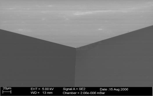
 GaAs / Ge *1 JFET on 4H-SiC-Wafer, thickness 160 µm with PCM (left upper rim) and back side metal, Dicing speed 200 mm/s")
6 Main Properties of TLS-Dicing Residue-free Zero kerf No chipping Nearly perfect sidewalls Works for back-side metal Works for: SiC Si (Semi & PV) GaAs / Ge *1 JFET on 4H-SiC-Wafer, thickness 160 µm with PCM (left upper rim) and back side metal, Dicing speed 200 mm/s 6
7 1. Thermal Laser Separation (TLS-Dicing ) 2. Application examples 3. microdice system 4. Conclusion
8 TLS-Dicing for SiC Exemplary Results Special USPs for SiC: Dicing speed 200 mm/s One cleaving pass per street PCM in street acceptable (no design rules) No tool wear Perfect side wall Further USPs: Back-side metal is separated w./o. pealing Tape not damaged *2 SiC-JFET, Wafer thickness 160 µm, Die size 3.16 X 3.16 mm², Back-side metal, mounted on DCB 8

9 Current (ma) TLS-Dicing Electrical Parameters for SiC *2 I-V blocking characteristics SiC JFET 1 SiC JFET 2 SiC JFET 3 SiC JFET 4 SiC JFET 5 10 *2 SiC-JFET, Wafer thickness 160 µm, Die size 3.16 X 3.16 mm², Back-side metal, mounted on DCB Voltage (V) No impact on electrical perfomance by TLS 9

10 TLS-Dicing Electrical Parameters for Si Project A cutting solar cell Project B Dicing of power-diodes HAZ from LEI *3 Cell Removed cell No HAZ from TLS Leakage current of diodes is significantly reduced TLS Electroluminescence measurement Damage free cutting through pn-junction is possible 10


11 TLS-Dicing Bending Stength *4 Comparison to ablative laser dicing 3 4x higher Resizing-ring (ø 300 to 200 mm, Si 775 µm) 11

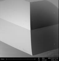
12 TLS-Dicing Separation of Back Side Metal Works with back side metal (up to 10 µm) Recommended: ratio metal to bulk: < 1 : 100 No peeling! *5 Si-Wafer with back side metal 12

13 TLS-Dicing Optical Properties One NIR cleaving-laser for all substrates For Si / Ge / GaAs / doped SiC a NIR-laser is optimal Different dopants are acceptable Scribing process option for PCM available *6 PCM / metal JFET- on 4H-SiC 13
14 TLS-Dicing for Other Materials *7 *9 *8 Si-Wafer Ge Si on glass 14
15 1. Thermal Laser Separation (TLS-Dicing ) 2. Application examples 3. microdice system 4. Conclusion
16 TLS-Dicing - Motivation SiC Dicing is a hard job (hardness 9.2 on Mohs scale) Cost High costs for saw blades Reduced uptime Quality Delamination of back side metal Defects by chipping Speed 2-10 mm/s Limited throughput 16

17 Our Solution microdice System for TLS-Dicing Lower cost, excellent cleaving results, and higher throughput 17
18 Advantages of TLS-Dicing Technology Cost reduction Minimal CoO due to contactless processing Increased yield by zero kerf Function Speed Excellent back-side metal separation Higher bending strength Dicing speed up to 300 mm/s Significant higher throughput 18
19 microdice System Up to 300 mm (12 ) wafer size Integrated laser sources with long lifetime Integrated patented micro stretching function Automated wafer handling SECS / GEM interface Compatible with common SEMI standards Consumables: only DI-water microdice 19
 Alignment system Vacuum chuck Handling unit (right side) 2 x 200 mm or 1 x 300 mm cassette Fault detection Major components")
20 microdice - Major Components Processing unit (left side) Scribing function (by pulsed fiber laser) Cleaving function (cw laser and cooling) Alignment system Vacuum chuck Handling unit (right side) 2 x 200 mm or 1 x 300 mm cassette Fault detection Major components 20


21 TLS-Dicing on microdice - a Case Study for SiC Current trends for SiC-products: The market volume of SiC is growing with CAGR of 25% One saw blade can t saw one 6 inch wafer 6 inch 4 inch Transition from 4 to 6 has been started 21
22 Advantage I - Throughput Wafer: 150 mm SiC Back side metal 160 µm thickness 1 mm die edge length PCM in street 70 µm street with Wafer p. h. mechanical saw TLS 4,3 Parameter: Speed 200 mm/s 0,4 mechanical saw TLS 22
23 Advantages II Reduced Footprint Saves Cost Footprint (m²) mechanical saw TLS 32 9 mechanical saw TLS Footprint for sawing 4 pieces 150 mm SiC-Wafer p.h (9 saws vs. 1 microdice ) 23

24 Assumptions for Cost Calculation Considered: Throughput: 4 wafer per hour Consumables (saw blades) Invest/depreciation for tool Footprint Not considered: Benefit in terms of yield Reduced operator costs mechanical saw: 37 TLS-Dicing :
25 1. Thermal Laser Separation (TLS-Dicing ) 2. Application examples 3. microdice system 4. Conclusion
26 Conclusion Minimal cost of ownership Clean process Better electrical properties High throughput Less breakage Increased yield Damage-free backside metal TLS-Dicing provides excellent cleaving results in combination with high yield and throughput. 26

27 TLS-Dicing - Cooperation with Fraunhofer IISB More then 8 years of successful cooperation *10 Experienced scientists Wide range of measurement tools Equipped with the latest version of TLS-Dicing tool in clean room TLS-Project partly funded by European contract SEA4KET 27
28 Image sources *1 Courtesy Fraunhofer Gesellschaft *2 Dohnke et. al: Comparison of different novel chip separation methods for 4H-SiC, Proceedings of ECSREAM conference, Grenoble 2014 *3 Koitzsch et. al.: Improving Electric Behavior and Simplifying Production of Si-Based Diodes by Using Thermal Laser Separation, Proceedings of ASMC2013, Saratoga Sprigs, (NY) *5 Karl Dohnke *4, 6-10 Courtesy Fraunhofer Gesellschaft 28

29 Thank you for your attention! 3D-Micromac AG Technologie-Campus Chemnitz, Germany Phone: info@3d-micromac.com 29 6/15/2016
High Yield Dicing of 100 mm and 150 mm SiC Wafer with High Throughput
 High Yield Dicing of 100 mm and 150 mm SiC Wafer with High Throughput Hans-Ulrich Zühlke (3D-Micromac, Chemnitz) Dirk Lewke (Fraunhofer IISB, Erlangen) Content 1. Motivation 2. Basics of TLS-Dicing 3.
Laser Micromachining for Industrial Applications and R&D. 3D-Micromac AG. Symposium on Smart Integrated Systems in Chemnitz. 3D-Micromac AG
 3D-Micromac AG Symposium on Smart Integrated Systems in Chemnitz 1 1 microdice - TLS-Dicing for separation of SiC 2 microprep - for high-throughput microstructure diagnostics 3 About 3D-Micromac AG 2 microdice
PDF created with FinePrint pdffactory Pro trial version
 Benefits Damage-free dicing of thin silicon Capable of producing smallest street widths which in return provides additional space for more parts per wafer Single step process results in reduction of cost
3D-Micromac AG. Micromachining Excellence
 3D-Micromac AG Micromachining Excellence Our international customers place great value on future-oriented and user-friendly processes. Our solutions help them increase production efficiency and lower cost.
Enabling Technology in Thin Wafer Dicing
 Enabling Technology in Thin Wafer Dicing Jeroen van Borkulo, Rogier Evertsen, Rene Hendriks, ALSI, platinawerf 2G, 6641TL Beuningen Netherlands Abstract Driven by IC packaging and performance requirements,
Abstract. Introduction
 Accelerating Silicon Carbide Power Electronics Devices into High Volume Manufacturing with Mechanical Dicing System By Meng Lee, Director, Product Marketing and Jojo Daof, Senior Process Engineer Abstract
ETIP-PV Manufacturing Conference Brussels, May 19 th Epitaxial Wafers: A game-changing technology on its way to mass production
 ETIP-PV Manufacturing Conference Brussels, May 19 th 2017 Epitaxial Wafers: A game-changing technology on its way to mass production NexWafe: producer of high-quality silicon wafers NexWafe will supply
Laser Dicing of Silicon: Comparison of Ablation Mechanisms with a Novel Technology of Thermally Induced Stress
 Dicing of Silicon: Comparison of Ablation Mechanisms with a Novel Technology of Thermally Induced Stress Oliver HAUPT, Frank SIEGEL, Aart SCHOONDERBEEK, Lars RICHTER, Rainer KLING, Andreas OSTENDORF Zentrum
Dicing Glass Optical Devices
 Glass Applications Dicing Glass Optical Devices -Blade Characteristics 2,, 4 4 Resin Type Q Diamond grit size: 15-45 mic. Thickness: 0.006-0.012 0.012 (0.15mm 0.3mm) Metal Sintered E08 & New matrices 8-258
Laser grooving technique for dicing nanoscale low-k wafer
 Laser grooving technique for dicing nanoscale low-k wafer Hsiang-Chen Hsu and Shih-Jeh Wu Professor Department of Mechanical and Automation Engineering I-Shou University HCHSU, ISU/Slide 1 Outline Background
Laser MicroJet. a technology for - prototyping - design innovation - mass customization - small / mid-sized manufacturing runs.
 Innovative Laser Systems Laser MicroJet a technology for - prototyping - design innovation - mass customization - small / mid-sized manufacturing runs Eric Krause EPMT EPHJ Swissphotonics seminar June
Optimizing the processing of sapphire with ultrashort laser pulses
 Optimizing the processing of sapphire with ultrashort laser pulses Geoff Lott 1, Nicolas Falletto 1, Pierre-Jean Devilder, and Rainer Kling 3 1 Electro Scientific Industries, Eolite Systems, 3 Alphanov
Power Electronics Packaging Solutions for Device Junction Temperature over 220 o C
 EPRC 12 Project Proposal Power Electronics Packaging Solutions for Device Junction Temperature over 220 o C 15 th August 2012 Page 1 Motivation Increased requirements of high power semiconductor device
Thin Wafers Bonding & Processing
 Thin Wafers Bonding & Processing A market perspective 2012 Why New Handling Technologies Consumer electronics is today a big driver for smaller, higher performing & lower cost device configurations. These
Surface Preparation Challenges in Crystalline Silicon Photovoltaic Manufacturing
 Surface Preparation Challenges in Crystalline Silicon Photovoltaic Manufacturing Kristopher Davis 1,3, Andrew C. Rudack 2,3, Winston Schoenfeld 1,3 Hubert Seigneur 1,3, Joe Walters 1,3, Linda Wilson 2,3
Innovative Laser Processing Technologies
 Innovative Laser Processing Technologies Reinhard Ferstl Director Sales & Marketing EMEA / Asia Corning Laser Technologies September 21, 2016 2016 Corning Incorporated Corning Market Segments and Additional
Atomic Oxygen-Resistant, Static-Dissipative, Pinhole-Free Coatings for Spacecraft
 Physical Sciences Inc. VG10-109 Atomic Oxygen-Resistant, Static-Dissipative, Pinhole-Free Coatings for Spacecraft Michelle T. Schulberg, Robert H. Krech, Frederick S. Lauten Physical Sciences Inc. Roy
Challenges for Embedded Device Technologies for Package Level Integration
 Challenges for Embedded Device Technologies for Package Level Integration Kevin Cannon, Steve Riches Tribus-D Ltd Guangbin Dou, Andrew Holmes Imperial College London Embedded Die Technology IMAPS-UK/NMI
Dicing of Ultra-thin Silicon Wafers
 Dicing of Ultra-thin Silicon Wafers Hans H. Gatzen, Gerald Guenzel Institute for Microtechnology, Hanover University, Germany Keywords: dicing, ultra thin wafers, silicon, chipping, machining Abstract:
Microwave Plasma Processing
 Microwave Plasma Processing MUEGGE GMBH Hochstraße 4-6 64385 Reichelsheim Fon +49 (0) 6164-93 07 11 Fax +49 (0) 6164-93 07 93 info@muegge.de www.muegge.de Microwave Plasma Processing Microwave Plasma Technology:
curamik CERAMIC SUBSTRATES AMB technology Design Rules Version #04 (09/2015)
") curamik CERAMIC SUBSTRATES AMB technology Design Rules Version #04 (09/2015) Content 1. Geometric properties 1.01. Available ceramic types / thicknesses... 03 1.02. thicknesses (standard)... 03 3. Quality
curamik CERAMIC SUBSTRATES AMB technology Design Rules Version #04 (09/2015) Content 1. Geometric properties 1.01. Available ceramic types / thicknesses... 03 1.02. thicknesses (standard)... 03 3. Quality
MRSI-175Ag Epoxy Dispenser
 MRSI-175Ag Epoxy Dispenser Applications: Microwave & RF Modules MEMS Semiconductor Packaging Multi-Chip Modules Hybrid Circuits Optical Modules Overview The MRSI-175Ag Conductive Epoxy Dispenser handles
EV Group 300mm Wafer Bonding Technology July 16, 2008
 EV Group 300mm Wafer Bonding Technology July 16, 2008 EV Group in a Nutshell st Our philosophy Our mission in serving next generation application in semiconductor technology Equipment supplier for the
AN Handling and processing of sawn wafers on UV dicing tape. Document information. Sawn wafers, UV dicing tape, handling and processing
 Handling and processing of sawn wafers on UV dicing tape Rev. 2.0 13 January 2009 Application note Document information Info Keywords Abstract Content Sawn wafers, UV dicing tape, handling and processing
Photolithography I ( Part 2 )
") 1 Photolithography I ( Part 2 ) Chapter 13 : Semiconductor Manufacturing Technology by M. Quirk & J. Serda Bjørn-Ove Fimland, Department of Electronics and Telecommunication, Norwegian University of Science
1 Photolithography I ( Part 2 ) Chapter 13 : Semiconductor Manufacturing Technology by M. Quirk & J. Serda Bjørn-Ove Fimland, Department of Electronics and Telecommunication, Norwegian University of Science
inemi ALTERNATIVE ENERGY WORKSHOP October 21, 2010 OPPORTUNITIES THROUGHOUT THE PHOTOVOLTAICS VALUE CHAIN
 inemi ALTERNATIVE ENERGY WORKSHOP October 21, 2010 OPPORTUNITIES THROUGHOUT THE PHOTOVOLTAICS VALUE CHAIN Prepared By: PRISMARK PARTNERS LLC 130 Main Street, Cold Spring Harbor NY 11724 USA Tel: 631 367-9187
Deep Silicon Etching An Enabling Technology for Wireless Systems Segment By Carson Ogilvie and Joel Goodrich Commercial Product Solutions
 Deep Silicon Etching An Enabling Technology for Wireless Systems Segment By Carson Ogilvie and Joel Goodrich Commercial Product Solutions Abstract The recent installation of a new etch tool, the Surface
Customizing Processes for Hermetic Assembly Of Devices Designed for Plastic Packages (1 of 3)
") Customizing Processes for Hermetic Assembly Of Devices Designed for Plastic Packages (1 of 3) Charlie C. Megia Golden Altos Corporation 402 South Hillview Drive, Milpitas, CA 95035 cmegia@goldenaltos.com
Customizing Processes for Hermetic Assembly Of Devices Designed for Plastic Packages (1 of 3) Charlie C. Megia Golden Altos Corporation 402 South Hillview Drive, Milpitas, CA 95035 cmegia@goldenaltos.com
High Throughput Laser Processing of Guide Plates for Vertical Probe Cards Rouzbeh Sarrafi, Dana Sercel, Sean Dennigan, Joshua Stearns, Marco Mendes
 High Throughput Laser Processing of Guide Plates for Vertical Probe Cards Rouzbeh Sarrafi, Dana Sercel, Sean Dennigan, Joshua Stearns, Marco Mendes IPG Photonics - Microsystems Division Outline Introduction
WATOM.. Wafer Topography Measurement KOCOS AUTOMATION GMBH [ ENG ]
![WATOM.. Wafer Topography Measurement KOCOS AUTOMATION GMBH [ ENG ]](/thumbs/75/71636806.jpg "WATOM.. Wafer Topography Measurement KOCOS AUTOMATION GMBH [ ENG ]") KO C O S - T H E T E C H N O L O G Y G R O U P W H E R E P R E C I S I O N M E E T S Q UA L I T Y WATOM.. Wafer Topography Measurement KOCOS AUTOMATION GMBH [ ENG ] C O N T E N T S WATOM... 3 Wafer edge
KO C O S - T H E T E C H N O L O G Y G R O U P W H E R E P R E C I S I O N M E E T S Q UA L I T Y WATOM.. Wafer Topography Measurement KOCOS AUTOMATION GMBH [ ENG ] C O N T E N T S WATOM... 3 Wafer edge
Solar Cells Fabrication Technologies
 Solar Cells Fabrication Technologies Crystalline Si Cell Technologies Amorphous Si Cell Technologies Thin Film Cell Technologies For a comprehensive tutorial on solar cells in general, see www.udel.edu/igert/pvcdrom
ANALYSING BACKSIDE CHIPPING ISSUES OF THE DIE AT WAFER SAW. Martin Vagues In Partial Fulfillment of MatE 234 May 10th, 2003
 ANALYSING BACKSIDE CHIPPING ISSUES OF THE DIE AT WAFER SAW Martin Vagues In Partial Fulfillment of MatE 234 May 10th, 2003 Prof Gunaselvaduray SJSU, San Jose ABSTRACT With shrinking technologies evolving,
bans the use of lead, mercury, cadmium, hexavalent chromium and polybrominated biphenyls (PBB) or polybrominated diphenyl ethers (PBDE).
 or polybrominated diphenyl ethers (PBDE).") MS7907 PRESSURE SENSOR DIE (0-7 BAR) 0 to 700 kpa range (7 bar or 102 PSI) Absolute/differential pressure sensors High linearity, small size RoHS-compatible & Pb-free 1 DESCRIPTION The sensor element of
MS7907 PRESSURE SENSOR DIE (0-7 BAR) 0 to 700 kpa range (7 bar or 102 PSI) Absolute/differential pressure sensors High linearity, small size RoHS-compatible & Pb-free 1 DESCRIPTION The sensor element of
3D technologies for integration of MEMS
 3D technologies for integration of MEMS, Fraunhofer Institute for Electronic Nano Systems Folie 1 Outlook Introduction 3D Processes Process integration Characterization Sample Applications Conclusion Folie
Development of an Low Cost Wafer Level Flip Chip Assembly Process for High Brightness LEDs Using the AuSn Metallurgy
 Development of an Low Cost Wafer Level Flip Chip Assembly Process for High Brightness LEDs Using the AuSn Metallurgy Gordon Elger, Rafael Jordan, Maria v. Suchodoletz and Hermann Oppermann Fraunhofer Institute
Optical Profilometry of Substrate Bow Reduction Using Temporary Adhesives
 Optical Profilometry of Substrate Bow Reduction Using Temporary Adhesives a Paul Flynn and b John Moore a FRT of America, LLC 1101 South Winchester Blvd., Suite L-240, San Jose, CA 95128 408-261-2632,
SEMICONDUCTOR WAFER-DIE SEPARATION SOLUTIONS
 UDM Systems, LLC SEMICONDUCTOR WAFER-DIE SEPARATION SOLUTIONS Advantages of UDM Systems Semiconductor Products UDM Systems, LLC products are specifically designed for use in multiple applications in semiconductor
AISI A2 Cold work tool steel
 T OOL STEEL FACTS AISI A2 Cold work tool steel Great Tooling Starts Here! General AISI A2 is an air- or oil hardening chromiummolybdenum-vanadium alloyed tool steel characterized by: Good machinability
PALISADE PD 40 SECTION SOLAR CONTROL FILMS. A. Optically clear Titanium Nitride ceramic sputtered polyester film for solar control.
 PART 1 GENERAL PALISADE PD 40 SECTION 08 87 13 SOLAR CONTROL FILMS 1.1 SUMMARY A. Optically clear Titanium Nitride ceramic sputtered polyester film for solar control. 1.2 RELATED SECTIONS A. Section 08
Simulation of Embedded Components in PCB Environment and Verification of Board Reliability
 Simulation of Embedded Components in PCB Environment and Verification of Board Reliability J. Stahr, M. Morianz AT&S Leoben, Austria M. Brizoux, A. Grivon, W. Maia Thales Global Services Meudon-la-Forêt,
1. Introduction. What is implantation? Advantages
 Ion implantation Contents 1. Introduction 2. Ion range 3. implantation profiles 4. ion channeling 5. ion implantation-induced damage 6. annealing behavior of the damage 7. process consideration 8. comparison
Micro and nano structuring of carbon based materials for micro injection moulding and hot embossing
 Micro and nano structuring of carbon based materials for micro injection moulding and hot embossing Victor Usov, Graham Cross, Neal O Hara, Declan Scanlan, Sander Paulen, Chris de Ruijter, Daniel Vlasveld,
Surface micromachining and Process flow part 1
 Surface micromachining and Process flow part 1 Identify the basic steps of a generic surface micromachining process Identify the critical requirements needed to create a MEMS using surface micromachining
Chapter 1.6. Polished Single-Crystal Silicon, Prime Wafers (all numbers nominal) Wafer Specification Table. Diameter 100 mm 4-inch 150 mm 6-inch
 Wafer Specification Table. Diameter 100 mm 4-inch 150 mm 6-inch") Chapter 1.6 I - Substrate Specifications Polished Single-Crystal Silicon, Prime Wafers (all numbers nominal) Wafer Specification Table Diameter 100 mm 4-inch 150 mm 6-inch Thickness 525 µm 20.5 mils 675
Chapter 1.6 I - Substrate Specifications Polished Single-Crystal Silicon, Prime Wafers (all numbers nominal) Wafer Specification Table Diameter 100 mm 4-inch 150 mm 6-inch Thickness 525 µm 20.5 mils 675
Silicon Wafer Processing PAKAGING AND TEST
 Silicon Wafer Processing PAKAGING AND TEST Parametrical test using test structures regularly distributed in the wafer Wafer die test marking defective dies dies separation die fixing (not marked as defective)
Transmission Mode Photocathodes Covering the Spectral Range
 Transmission Mode Photocathodes Covering the Spectral Range 6/19/2002 New Developments in Photodetection 3 rd Beaune Conference June 17-21, 2002 Arlynn Smith, Keith Passmore, Roger Sillmon, Rudy Benz ITT
Ceramos Gen 5 Details on Handling and Processing Application Note
 Ceramos Gen 5 Details on Handling and Processing Application Note Abstract This application note provides information on handling and processing of the CERAMOS Gen5 (CUW CFUP). CERAMOS Gen5 CUW CFUP The
Glass Breakage Failure Mode and Stress Estimation
 In most cases, forensic analysis of the fracture origin, also known as the break origin, can provide useful information about the glass breakage and often the root cause of the breakage. If the break origin
Chips Face-up Panelization Approach For Fan-out Packaging
 Chips Face-up Panelization Approach For Fan-out Packaging Oct. 15, 2015 B. Rogers, D. Sanchez, C. Bishop, C. Sandstrom, C. Scanlan, TOlson T. REV A Background on FOWLP Fan-Out Wafer Level Packaging o Chips
Suncycle GmbH. Service overview
 Suncycle GmbH Service overview 01 Suncycle Suncycle offers specialized test and repair services for the solar industry. With more than 3 million repaired modules owns Suncycle an unique experience in customer
Leveraging the Precision of Electroforming over Alternative Processes When Developing Nano-scale Structures
 VOLUME 4 - ELECTROFORMING Leveraging the Precision of over Alternative Processes When Developing Nano-scale Structures Electrical and mechanical component and subsystem designers generally have five techniques
Die Hardfacing and Remanufacturing using Direct Metal Deposition (DMD) B. Dutta POM Group, Inc., Auburn Hills, MI-48326
 B. Dutta POM Group, Inc., Auburn Hills, MI-48326") Die Hardfacing and Remanufacturing using Direct Metal Deposition (DMD) B. Dutta POM Group, Inc., Auburn Hills, MI-48326 OUTLINE Company Overview of Direct Metal Deposition DMD Systems DMD Application in
Die Hardfacing and Remanufacturing using Direct Metal Deposition (DMD) B. Dutta POM Group, Inc., Auburn Hills, MI-48326 OUTLINE Company Overview of Direct Metal Deposition DMD Systems DMD Application in
photovoltaics services Photovoltaics Analysis, Testing, certification gain access to global PhotoVoltaic markets
 ELECTRICAL & ELECTRONICS photovoltaics services Photovoltaics Analysis, Testing, certification gain access to global PhotoVoltaic markets LOCALLY AVAILABLE worldwide Electrical and electronic product manufacturers
IMPLEMENTATION OF A FULLY MOLDED FAN-OUT PACKAGING TECHNOLOGY
 IMPLEMENTATION OF A FULLY MOLDED FAN-OUT PACKAGING TECHNOLOGY B. Rogers, C. Scanlan, and T. Olson Deca Technologies, Inc. Tempe, AZ USA boyd.rogers@decatechnologies.com ABSTRACT Fan-Out Wafer-Level Packaging
School of Photovoltaic and Renewable Energy Engineering
 School of Photovoltaic and Renewable Energy Engineering Silicon PV Education, Research and Industry in Australia R. Corkish, Head of School r.corkish@unsw.edu.au www.pv.unsw.edu.au Photo: K. McLean Context:
Tackling the optical interconnection challenge for the Integrated Photonics Revolution
 Tackling the optical interconnection challenge for the Integrated Photonics Revolution Dr. Ir. TU Delft, Precision and Microsystems Engineering m.tichem@tudelft.nl Microfabrication and MEMS Si microfabrication
Kerf! Microns. Driving Forces Impact of kerf is substantial in terms of silicon usage 50 % of total thickness for 100 mm wafers
 2nd. Annual c-si PVMC Workshop at Intersolar NA, San Francisco, CA, July 2013 1 Microns Kerf! Driving Forces Impact of kerf is substantial in terms of silicon usage 50 % of total thickness for 100 mm wafers
Packaging Technologies for SiC Power Modules
 Packaging Technologies for SiC Power Modules Masafumi Horio Yuji Iizuka Yoshinari Ikeda ABSTRACT Wide bandgap materials such as silicon carbide (SiC) and gallium nitride (GaN) are attracting attention
Recent Advances in Die Attach Film
 Recent Advances in Die Attach Film Frederick Lo, Maurice Leblon, Richard Amigh, and Kevin Chung. AI Technology, Inc. 70 Washington Road, Princeton Junction, NJ 08550 www.aitechnology.com Abstract: The
A Deep Silicon RIE Primer Bosch Etching of Deep Structures in Silicon
 A Deep Silicon RIE Primer Bosch Etching of Deep Structures in Silicon April 2009 A Deep Silicon RIE Primer 1.0) Etching: Silicon does not naturally etch anisotropically in fluorine based chemistries. Si
IISW-2009 BSI technical challenges
 IISW-2009 BSI technical challenges Bergen. 25th June 2009 Outline BSI consumer vs BSI scientific BSI vs FSI Remaining challenges Charges collection BSI overlay challenges BSI laser annealing Thinning Process
MTS Semiconductor Solution
 MTS 0 unplanned down time Solution Lowest operating Cost Solution Energy saving Solution Equipment Fine Pitch and UPH Upgrade solution Quality & Yield Improvement Solution Reliability Enhancement Solution
PROVIDER OF BREAKTHROUGH TECHNOLOGY, PROCESSES AND EQUIPMENT FOR ENGINEERED SUBSTRATE SOLUTIONS. ...
 SEMICONDUCTOR SOLAR DISPLAY OPTOELECTRONIC PROVIDER OF BREAKTHROUGH TECHNOLOGY, PROCESSES AND EQUIPMENT FOR ENGINEERED SUBSTRATE SOLUTIONS........... A Look at Silicon Genesis 1997 Founded as a fabless
Fabrication Technology
 Fabrication Technology By B.G.Balagangadhar Department of Electronics and Communication Ghousia College of Engineering, Ramanagaram 1 OUTLINE Introduction Why Silicon The purity of Silicon Czochralski
Quality in Electronic Production has a Name: Viscom. System Overview
 Quality in Electronic Production has a Name: Viscom System Overview Successful along the whole line with Viscom Circuit board manufacturing Paste print Finish S3070 AFI-Scan S3054QS Paste print Thick film
Plasma Etching Rates & Gases Gas ratios affects etch rate & etch ratios to resist/substrate
 Plasma Etching Rates & Gases Gas ratios affects etch rate & etch ratios to resist/substrate Development of Sidewalls Passivating Films Sidewalls get inert species deposited on them with plasma etch Creates
Test Flow for Advanced Packages (2.5D/SLIM/3D)
") 1 Test Flow for Advanced Packages (2.5D/SLIM/3D) Gerard John Amkor Technology Inc. Gerard.John@amkor.com 2045 East Innovation Circle, Tempe, AZ 85284, USA Phone: (480) 821-5000 ADVANCED PACKAGE TEST FLOW
1 Test Flow for Advanced Packages (2.5D/SLIM/3D) Gerard John Amkor Technology Inc. Gerard.John@amkor.com 2045 East Innovation Circle, Tempe, AZ 85284, USA Phone: (480) 821-5000 ADVANCED PACKAGE TEST FLOW
Laser Spike Annealing for sub-20nm Logic Devices
 Laser Spike Annealing for sub-20nm Logic Devices Jeff Hebb, Ph.D. July 10, 2014 1 NCCAVS Junction Technology Group Semicon West Meeting July 10, 2014 Outline Introduction Pattern Loading Effects LSA Applications
TSV Processing and Wafer Stacking. Kathy Cook and Maggie Zoberbier, 3D Business Development
 TSV Processing and Wafer Stacking Kathy Cook and Maggie Zoberbier, 3D Business Development Outline Why 3D Integration? TSV Process Variations Lithography Process Results Stacking Technology Wafer Bonding
8. Epitaxy. - Extended single-crystal film formation on top of a crystalline substrate
 8. Epitaxy 1. Introduction επι(epi placed or resting upon) ταξιζ(taxis arrangement) - Extended single-crystal film formation on top of a crystalline substrate - Homoepitaxy : Film and substrate are the
Applications of Systems for Beam Shaping in Material Processing Pulsar Photonics GmbH
 LASER World of Photonics 2015 Workshop Using Diffractive Optics Applications of Systems for Beam Shaping in Material Processing Pulsar Photonics GmbH Speaker Dipl. Phys. Stephan Eifel, Pulsar Photonics
NanoSystemsEngineering: NanoNose Final Status, March 2011
 1 NanoSystemsEngineering: NanoNose Final Status, March 2011 The Nanonose project is based on four research projects (VCSELs, 3D nanolithography, coatings and system integration). Below, the major achievements
Lab #2 Wafer Cleaning (RCA cleaning)
") Lab #2 Wafer Cleaning (RCA cleaning) RCA Cleaning System Used: Wet Bench 1, Bay1, Nanofabrication Center Chemicals Used: H 2 O : NH 4 OH : H 2 O 2 (5 : 1 : 1) H 2 O : HF (10 : 1) H 2 O : HCl : H 2 O 2
Lab #2 Wafer Cleaning (RCA cleaning) RCA Cleaning System Used: Wet Bench 1, Bay1, Nanofabrication Center Chemicals Used: H 2 O : NH 4 OH : H 2 O 2 (5 : 1 : 1) H 2 O : HF (10 : 1) H 2 O : HCl : H 2 O 2
LED Die Attach Selection Considerations
 LED Die Attach Selection Considerations Gyan Dutt & Ravi Bhatkal Alpha, An Alent plc Company Abstract Die attach material plays a key role in performance and reliability of mid, high and super-high power
Intel Pentium Processor W/MMX
 Construction Analysis Intel Pentium Processor W/MMX Report Number: SCA 9706-540 Global Semiconductor Industry the Serving Since 1964 15022 N. 75th Street Scottsdale, AZ 85260-2476 Phone: 602-998-9780 Fax:
Aluminum / Copper oscillation welding with a 500 W direct diode laser
 Application Note Issued: 2016-06-01 Aluminum / Copper oscillation welding with a 500 W direct diode laser SUMMARY The performance of the 500 W DirectProcess direct diode laser for oscillating welding by
Precision Electroforming in High-Strength NiColoy
 Taking the Stress out of Electroforming www.nicoform.com Precision Electroforming in High-Strength NiColoy Copyright 2007 NiCoForm, Inc. (Rochester, NY) Electroforming What is it? What is it good for?
CHARACTERISATION OF INTERFACIAL CRACKING IN MICROELECTRONIC PACKAGING
 CHARACTERISATION OF INTERFACIAL CRACKING IN MICROELECTRONIC PACKAGING Ian McEnteggart Microelectronics Business Manager Instron Limited, Coronation Road, High Wycombe, Buckinghamshire HP12 3SY www.instron.com/microelectronics
CSI GUIDE Countertops
 CSI GUIDE Countertops Part 1 General 1.0 RELATED DOCUMENTS A. Drawings and general provisions of the contract, including general and supplementary conditions and Division 1 Specification Sections, apply
Microstructuring of Steel and Hard Metal using Femtosecond Laser Pulses
 Available online at www.sciencedirect.com Physics Procedia 12 (2011) 60 66 LiM 2011 Microstructuring of Steel and Hard Metal using Femtosecond Laser Pulses Manuel Pfeiffer a *, Andy Engel a, Steffen Weißmantel
FOBA Y-Series. High potential fiber marking lasers: More clarity, less complexity. Your product benefits
 FOBA Y-Series High potential fiber marking lasers: More clarity, less complexity Laser marking has become one of the preferred methods for product identification, decoration and material processing. Many
How can MOCVD enable production of cost efficient HB LED's
 How can MOCVD enable production of cost efficient HB LED's Dr. Frank Schulte AIXTRON SE Company and Market Market requests and challenges Answer from the technology Conclusion P 2 Confidential Proprietary
Technical challenges in car glass bending
 Technical challenges in car glass bending 1 st Glass bending seminare Author: Frank De Ridder Bekaert/Bekintex Summary Trends & needs in automotive glass Heat resistant textile products & applications
Performance Improvements in PV Modules Using Ionomer Encapsulants
 Performance Improvements in PV Modules Using Ionomer Encapsulants Mark Jacobson Sr. Accounts Manager, DuPont Encapsulants Cleveland, OH April 9, 2011 2 Agenda Encapsulant requirements Failure modes Moisture
Ceramic Microchannel Devices for Thermal Management. C. Lewinsohn, J. Fellows, and H. Anderson Ceramatec, Inc. Salt Lake City, UT
 Ceramic Microchannel Devices for Thermal Management C. Lewinsohn, J. Fellows, and H. Anderson Ceramatec, Inc. Salt Lake City, UT The Right Size for The Right Physics centi milli micro 2 Multiscale Structure
3.46 OPTICAL AND OPTOELECTRONIC MATERIALS
 Badgap Engineering: Precise Control of Emission Wavelength Wavelength Division Multiplexing Fiber Transmission Window Optical Amplification Spectrum Design and Fabrication of emitters and detectors Composition
Roll-to-roll Technology for Transparent High Barrier Films
 Roll-to-roll Technology for Transparent High Barrier Films Presented at the AIMCAL Fall Technical Conference, October 19-22, 2008, Myrtle Beach, SC, USA Nicolas Schiller, John Fahlteich, Matthias Fahland,
GLOBAL QUALITY SOLUTIONS PACKAGE INTEGRITY SEAL INTEGRITY LEAK DETECTION
 GLOBAL QUALITY SOLUTIONS PACKAGE INTEGRITY SEAL INTEGRITY LEAK DETECTION Redefining the standards for accuracy and reliability. About PTI PTI Packaging Technologies & Inspection is headquartered in Tuckahoe,
Inline-high-rate thermal evaporation of aluminum for novel industrial solar cell metallization
 2nd Workshop on Metallization Konstanz, April 14 th -15 th, 2010 Inline-high-rate thermal evaporation of aluminum for novel industrial solar cell metallization Frank Heinemeyer 1 Motivation Development
Wafer Marking & Wafer Sorting Solutions
 Wafer Marking & Wafer Sorting Solutions General High Quality Wafer Marking & Sorting Solutions for the Semiconductor Industry History InnoLas GmbH was founded on January 1, 1995 by Andreas Behr, Reinhard
Key words: microprocessor integrated heat sink Electronic Packaging Material, Thermal Management, Thermal Conductivity, CTE, Lightweight
 Aluminum Silicon Carbide (AlSiC) Microprocessor Lids and Heat Sinks for Integrated Thermal Management Solutions Mark A. Occhionero, Robert A. Hay, Richard W. Adams, Kevin P. Fennessy, and Glenn Sundberg
Development of High-concentration Photovoltaics at Fraunhofer ISE: Cells and Systems
 Development of High-concentration Photovoltaics at Fraunhofer ISE: Cells and Systems Gerhard Peharz Fraunhofer-Institut für Solare Energiesysteme ISE 23 rd October 2008 Outline The Fraunhofer ISE III-V
Lecture 5. SOI Micromachining. SOI MUMPs. SOI Micromachining. Silicon-on-Insulator Microstructures. Agenda:
 EEL6935 Advanced MEMS (Spring 2005) Instructor: Dr. Huikai Xie SOI Micromachining Agenda: SOI Micromachining SOI MUMPs Multi-level structures Lecture 5 Silicon-on-Insulator Microstructures Single-crystal
THE NEXT GENERATION OF GERMANIUM SUBSTRATES: EXPOGER
 THE NEXT GENERATION OF GERMANIUM SUBSTRATES: EXPOGER Pieter Arickx (1), Rufi Kurstjens (1), Wim Geens (1), Kristof Dessein (1) (1) Umicore Electro-Optic Materials, Watertorenstraat 33 B2250 Olen (Belgium),
Project EFFORTLESS. Epitaxy Factory of the Future for Transformational Leverage of Europe s Compound Semiconductor EcoSystem
 Project EFFORTLESS Epitaxy Factory of the Future for Transformational Leverage of Europe s Compound Semiconductor EcoSystem Domain: Process Technologies supplying Smart Health, Energy, Manufacturing and
1/2W, 0805 Low Resistance Chip Resistor (Lead / Halogen free)
") 1. Scope 1/2W, 0805 (Lead / Halogen free) This specification applies to 1.2mm x 2.0mm size 1/2W, fixed metal film chip resistors rectangular type for use in electronic equipment. 2. Type Designation RL
1. Scope 1/2W, 0805 (Lead / Halogen free) This specification applies to 1.2mm x 2.0mm size 1/2W, fixed metal film chip resistors rectangular type for use in electronic equipment. 2. Type Designation RL
Semicon Europa Wafer Chucks for Lithography. Berliner Glas KGaA Herbert Kubatz GmbH & Co. Sven Götze
 Semicon Europa 2011. Wafer Chucks for Lithography. Berliner Glas KGaA Herbert Kubatz GmbH & Co. Sven Götze 1 Export driven, medium-sized, innovative. Solutions in Optics High Tech in Glass Legal form:
Turn-key Production System for Solar Cells
 SOLARE Turn-key Production System for Solar Cells 02 Innovations for New Technologies provides technology solutions for both crystalline and thin-film highperformance solar cell platforms. Our production
Dicing of Gallium Arsenide (GaAs) Wafers with the Laser MicroJet Challenges, Improvements and Safety Issues
 Wafers with the Laser MicroJet Challenges, Improvements and Safety Issues") Dicing of Gallium Arsenide (GaAs) Wafers with the Laser MicroJet Challenges, Improvements and Safety Issues Natalia M. Dushkina Laboratory of Laser Applications, The Gem City Engineering Co. Dayton, Ohio
Dicing of Gallium Arsenide (GaAs) Wafers with the Laser MicroJet Challenges, Improvements and Safety Issues Natalia M. Dushkina Laboratory of Laser Applications, The Gem City Engineering Co. Dayton, Ohio
Hot Chips: Stacking Tutorial
 Hot Chips: Stacking Tutorial Choon Lee Technology HQ, Amkor Enabling a Microelectronic World Mobile Phone Technology Change Feature Phone Smartphone Smartphones as a Percentage of All Phones Source : The