ALD systems and SENTECH Instruments GmbH
|
|
|
- Candice Wilkerson
- 6 years ago
- Views:
Transcription
1 ALD systems and SENTECH Instruments GmbH H. Gargouri, F. Naumann, R. Rudolph and M. Arens SENTECH Instruments GmbH, Berlin 1
2 2 Agenda 1. Company Introduction 2. SENTECH-ALD-Systems 3. Process Results Plasma Processes In-situ Ellipsometry 4. Summary and Outlook
 ISO 9001 certificated Business fields: Thin Film Metrology & Plasma Process Technology")

3 3 The Company Private company founded in 1990 New building since employees (~ 25 % R & D) ISO 9001 certificated Business fields: Thin Film Metrology & Plasma Process Technology More than 1,500 metrology tools and 300 plasma tools in the field SENTECH s strengths: Application support Broad range of products High quality of products Service Turn over 2012: 10 Mio Euro

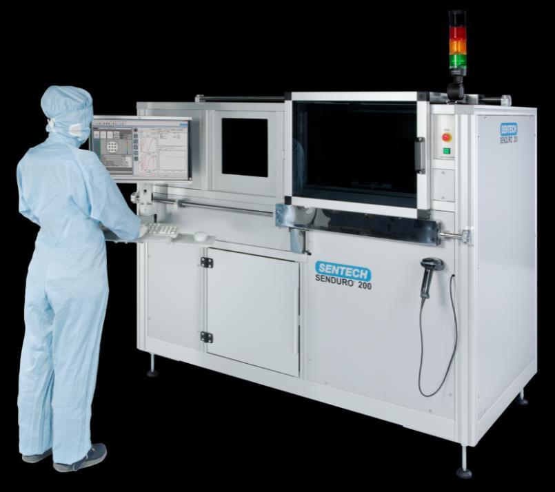


4 Thin Film Metrology Instruments: Reflectometers Laser ellipsometers Spectroscopic ellipsometers (deep UV MIR) in-situ measurement tools For more information, please visit us in hall 1 / stand


5 Plasma ALD Plasma Process Technology Plasma deposition Cluster tool RIE, ICP-RIE PECVD, ICPECVD Cluster tools ALD / PEALD SENTECH laser end point monitor For more information, please visit us in hall 1 / stand Plasma etching 5
6 6 Agenda 1. Company Introduction 2. SENTECH-ALD-Systems 3. Process Results Plasma Processes In-situ Ellipsometry 4. Summary and Outlook


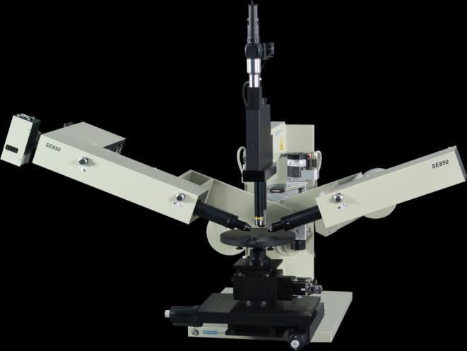
7 7 SI ALD systems SI ALD LL SI ALD

8 8 Reactor chamber and plasma source - Reactor chamber Temperature: up to 150 C Showerhead mode - Precursor line Temperature: up to 200 C 3-Port ALD-valve Stop valve - Plasma source True remote CCP-source isolation valve Plasma source can be separated from the system

9 9 System and options - Substrate size up to 8 - Substrate temperature up to 500 C SI ALD LL with SENTECH In situ ellipsometer - Precursor lines up to 4 separate inlets More precursors with common inlet Direct draw or bubble line - Gas lines up to 7 - In-situ diagnostic SENTECH ellipsometer QMS, - More options TMP with isolation valve Ozone line Glove box
10 10 Agenda 1. Company Introduction 2. SENTECH-ALD-Systems 3. Process Results Plasma Processes In-situ Ellipsometry 4. Summary and Outlook

11 11 Selected processes Thermal deposition: Al 2 O 3 200, 100 C 200 C ZrO C Plasma enhanced deposition: Al 2 O C 27 C SiO C TiO C 250 C 200 C
12 12 ALD and PEALD Al 2 O 3 in SI ALD LL - Al 2 O 3 film thickness shows linear dependence on the number of cycles in ALD and PEALD. - PEALD provides a higher growth rate of 1,2 Å/cycle compared to ALD. The growth rate in ALD amounts 0,8 Å/cycle. Process parameter ALD PEALD Substrate temperature ( C) Process pressure (Pa) Plasma power (W) Growth rate (Å/Cycle) 0,8 1,2
13 13 ALD and PEALD Al 2 O 3 in SI ALD LL Homogeneity Refractive index - ALD and PEALD Al 2 O 3 films show very good homogeneity (range, not sigma!) of ± 0,6 % and ± 0,9 % on 4 Si-wafer respectively. - Refractive indexes 632,8 nm wavelength) of ALD and PEALD Al 2 O 3 films with the same thickness are identical.
![Druck [Pa] www.sentech.](/docs-images/77/75892459/images/14-1.jpg "de 14 Multilayer Al 2 O 3 / SiO 2 - thermal ALD Al 2 O 3 and PEALD SiO 2 alternately - in total 44 layers : 23 Al 2 O 3 -layers and 21 SiO 2 -layers (~ 1 µm) - deposition time: ~ 14 h 30 Layer")
14 Druck [Pa] 14 Multilayer Al 2 O 3 / SiO 2 - thermal ALD Al 2 O 3 and PEALD SiO 2 alternately - in total 44 layers : 23 Al 2 O 3 -layers and 21 SiO 2 -layers (~ 1 µm) - deposition time: ~ 14 h 30 Layer thickness (SENTECH Reflectometer: RM 2000) SiO 2 -Process Al 2 O 3 -Process Zeit [h] Excellent homogeneity (± 0,6 %, 4 -Wafer) Very good agreement with expected film thickness
 1,2 Substrate temperature ( C) 200 n (@632,8 nm) 1,642 (± 0,58%) Layer thickness: 8 wafer (nm) 40,8 (± 1,96%) Growth rate (Å/cycle) 0,9 Substrate temperature ( C) 250 n (@632,8 nm) 1,933")
15 15 PEALD on 8" Wafer Al 2 O 3 : TMA + O 2 -Plasma AlN: TMA + NH 3 -Plasma SENTECH Ellipsometer: SE 800 SENTECH Ellipsometer: SE 800 Layer thickness: 8 wafer (nm) 26,8 (± 1,6%) Growth rate (Å/cycle) 1,2 Substrate temperature ( C) 200 n (@632,8 nm) 1,642 (± 0,58%) Layer thickness: 8 wafer (nm) 40,8 (± 1,96%) Growth rate (Å/cycle) 0,9 Substrate temperature ( C) 250 n (@632,8 nm) 1,933 (± 0,91%)
16 16 In-situ methods in situ monitoring during ALD-processes require fast and sensitive methods different methods have been applied like QCM, QMS, ellipsometry. best suited for layer monitoring is ellipsometry due to the high surface sensitivity ellipsometry does not influence the processs and measures directly the layer properties
17 17 In-situ ellipsometry of Al 2 O 3 growth Thermal deposition growth monitoring extremely sensitive even different steps in cycle visible
18 18 In-situ monitoring of PEALD-TiO 2 In-situ end point detection possible on sub Å-scale
 Prepared samples were treated with O 2 -plasma to remove resist and examined with REM*. Very good conformality to 3D structures *) Thanks to Dr.")
19 19 Conformality 18 nm ALD-Al 2 O 80 C 21 nm PEALD-Al 2 O 80 C 1) 3D resist structures were prepared on Si-Wafers* and coated with ALD and PEALD Al 2 O 3 at 80 C substrate temperature. 2) Prepared samples were treated with O 2 -plasma to remove resist and examined with REM*. Very good conformality to 3D structures *) Thanks to Dr. Hübner, IPHT-Jena, Germany, for preparing the 3D structures and doing the REM-measurement.


20 20 Summary Outstanding features of SI ALD-systems: Flexible system configuration for a wide range of processes and applications Rugged design and small footprint Outlook - Process results: PEALD-Processes: excellent uniformity SENTECH in-situ ellipsometry: very sensitive for monitoring of thin layer growth Further thermal and plasma enhanced processes and applications - Nitride and metal deposition - Coating of different substrates and structures - Optimization of in-situ measurement for better process understanding

 SENTECH")
21 21 Thank you for your attention. SENTECH GmbH (Krailling bei München) SENTECH Instruments GmbH (Berlin)
Low temperature deposition of thin passivation layers by plasma ALD
 1 Low temperature deposition of thin passivation layers by plasma ALD Bernd Gruska, SENTECH Instruments GmbH, Germany 1. SENTECH in brief 2. Low temperature deposition processes 3. SENTECH SI ALD LL System
micro resist technology
 Characteristics Processing guidelines Negative Tone Photoresist Series ma-n 2400 ma-n 2400 is a negative tone photoresist series designed for the use in micro- and nanoelectronics. The resists are available
Processing guidelines. Negative Tone Photoresist Series ma-n 2400
 Characteristics Processing guidelines Negative Tone Photoresist Series ma-n 2400 ma-n 2400 is a negative tone photoresist series designed for the use in micro- and nanoelectronics. The resists are available
Method to obtain TEOS PECVD Silicon Oxide Thick Layers for Optoelectronics devices Application
 Method to obtain TEOS PECVD Silicon Oxide Thick Layers for Optoelectronics devices Application ABSTRACT D. A. P. Bulla and N. I. Morimoto Laboratório de Sistemas Integráveis da EPUSP São Paulo - S.P. -
Fiji Thermal and Plasma Atomic Layer Deposition System (ALD) By Ultratech (Cambridge)
 By Ultratech (Cambridge)") Fiji Thermal and Plasma Atomic Layer Deposition System (ALD) By Ultratech (Cambridge) PREPARED BY: You-Sheng (Wilson) Lin, Nanolab Staff 7-30-2013 Superusers: Steve Franz You-Sheng Lin Max Ho X68923 X68923
Fiji Thermal and Plasma Atomic Layer Deposition System (ALD) By Ultratech (Cambridge) PREPARED BY: You-Sheng (Wilson) Lin, Nanolab Staff 7-30-2013 Superusers: Steve Franz You-Sheng Lin Max Ho X68923 X68923
200mm Next Generation MEMS Technology update. Florent Ducrot
 200mm Next Generation MEMS Technology update Florent Ducrot The Most Exciting Industries on Earth Semiconductor Display Solar 20,000,000x reduction in COST PER TRANSISTOR in 30 years 1 20x reduction in
New Materials as an enabler for Advanced Chip Manufacturing
 New Materials as an enabler for Advanced Chip Manufacturing Drive Innovation, Deliver Excellence ASM International Analyst and Investor Technology Seminar Semicon West July 10 2013 Outline New Materials:
Flexible functional devices at mass production level with the FLEx R2R sald platform
 Flexible functional devices at mass production level with the FLEx R2R sald platform D. Spee, W. Boonen, D. Borsa and E. Clerkx Meyer Burger (Netherlands) B.V. Meyer Burger Introduction to sald Challenges
Procese de depunere in sistemul Plasma Enhanced Chemical Vapor Deposition (PECVD)
") Procese de depunere in sistemul Plasma Enhanced Chemical Vapor Deposition (PECVD) Ciprian Iliescu Conţinutul acestui material nu reprezintă in mod obligatoriu poziţia oficială a Uniunii Europene sau a
Procese de depunere in sistemul Plasma Enhanced Chemical Vapor Deposition (PECVD) Ciprian Iliescu Conţinutul acestui material nu reprezintă in mod obligatoriu poziţia oficială a Uniunii Europene sau a
Ultra High Barrier Coatings by PECVD
 Society of Vacuum Coaters 2014 Technical Conference Presentation Ultra High Barrier Coatings by PECVD John Madocks & Phong Ngo, General Plasma Inc., 546 E. 25 th Street, Tucson, Arizona, USA Abstract Silicon
Supporting Information
 Supporting Information Fast-Response, Sensitivitive and Low-Powered Chemosensors by Fusing Nanostructured Porous Thin Film and IDEs-Microheater Chip Zhengfei Dai,, Lei Xu,#,, Guotao Duan *,, Tie Li *,,
A Deep Silicon RIE Primer Bosch Etching of Deep Structures in Silicon
 A Deep Silicon RIE Primer Bosch Etching of Deep Structures in Silicon April 2009 A Deep Silicon RIE Primer 1.0) Etching: Silicon does not naturally etch anisotropically in fluorine based chemistries. Si
Fundamental Aspects of Atomic Layer Deposition (ALD) and Molecular Layer Deposition (MLD) Micro/Nano-Electromechanical Transducers (imint) 2
 and Molecular Layer Deposition (MLD) Micro/Nano-Electromechanical Transducers (imint) 2") Fundamental Aspects of Atomic Layer Deposition (ALD) and Molecular Layer Deposition (MLD) Steven M. George 1,2,3, Victor M. Bright 1,4,Y. C. Lee 1,4 1 DARPA Center on Science and Technology for Integrated
Fundamental Aspects of Atomic Layer Deposition (ALD) and Molecular Layer Deposition (MLD) Steven M. George 1,2,3, Victor M. Bright 1,4,Y. C. Lee 1,4 1 DARPA Center on Science and Technology for Integrated
Lecture Day 2 Deposition
 Deposition Lecture Day 2 Deposition PVD - Physical Vapor Deposition E-beam Evaporation Thermal Evaporation (wire feed vs boat) Sputtering CVD - Chemical Vapor Deposition PECVD LPCVD MVD ALD MBE Plating
How can MOCVD enable production of cost efficient HB LED's
 How can MOCVD enable production of cost efficient HB LED's Dr. Frank Schulte AIXTRON SE Company and Market Market requests and challenges Answer from the technology Conclusion P 2 Confidential Proprietary
ME 141B: The MEMS Class Introduction to MEMS and MEMS Design. Sumita Pennathur UCSB
 ME 141B: The MEMS Class Introduction to MEMS and MEMS Design Sumita Pennathur UCSB Outline today Introduction to thin films Oxidation Deal-grove model CVD Epitaxy Electrodeposition 10/6/10 2/45 Creating
State of the art quality of a GeOx interfacial passivation layer formed on Ge(001)
") APPLICATION NOTE State of the art quality of a Ox interfacial passivation layer formed on (001) Summary A number of research efforts have been made to realize Metal-Oxide-Semiconductor Field Effect Transistors
APPLICATION NOTE State of the art quality of a Ox interfacial passivation layer formed on (001) Summary A number of research efforts have been made to realize Metal-Oxide-Semiconductor Field Effect Transistors
5.8 Diaphragm Uniaxial Optical Accelerometer
 5.8 Diaphragm Uniaxial Optical Accelerometer Optical accelerometers are based on the BESOI (Bond and Etch back Silicon On Insulator) wafers, supplied by Shin-Etsu with (100) orientation, 4 diameter and
Pioneering ALD experience since The ALD Powerhouse PRODUCT CATALOGUE FOR SUNALE P-SERIES ALD SYSTEMS
 Pioneering ALD experience since 1974 The ALD Powerhouse PRODUCT CATALOGUE FOR SUNALE P-SERIES ALD SYSTEMS SUNALE P-SERIES ALD SYSTEMS PRODUCT CATALOGUE Description SUNALE P-series ALD system SUNALE P-series
ALD and CVD of Copper-Based Metallization for. Microelectronic Fabrication. Department of Chemistry and Chemical Biology
 ALD and CVD of Copper-Based Metallization for Microelectronic Fabrication Yeung Au, Youbo Lin, Hoon Kim, Zhengwen Li, and Roy G. Gordon Department of Chemistry and Chemical Biology Harvard University Introduction
Application of ultra-thin aluminum oxide etch mask made by atomic layer deposition technique
 IOP Publishing Journal of Physics: Conference Series 61 (2007) 369 373 doi:10.1088/1742-6596/61/1/074 International Conference on Nanoscience and Technology (ICN&T 2006) Application of ultra-thin aluminum
EXCIMER LASER ANNEALING FOR LOW- TEMPERATURE POLYSILICON THIN FILM TRANSISTOR FABRICATION ON PLASTIC SUBSTRATES
 EXCIMER LASER ANNEALING FOR LOW- TEMPERATURE POLYSILICON THIN FILM TRANSISTOR FABRICATION ON PLASTIC SUBSTRATES G. Fortunato, A. Pecora, L. Maiolo, M. Cuscunà, D. Simeone, A. Minotti, and L. Mariucci CNR-IMM,
Overview of ALD-Activities for Optical Applications: Materials, Refractive and Diffractive Optics
 Overview of ALD-Activities for Optical Applications: Materials, Refractive and Diffractive Optics Adriana Szeghalmi, 1,2, S. Shestaeva 1, Astrid Bingel 1 L. Ghazaryan 2, K. Pfeiffer 2, S. Ratzsch 2 1 Fraunhofer
Surface Preparation and Cleaning Conference April 19-20, 2016, Santa Clara, CA, USA. Nano-Bio Electronic Materials and Processing Lab.
 Surface Preparation and Cleaning Conference April 19-20, 2016, Santa Clara, CA, USA Issues on contaminants on EUV mask Particle removal on EUV mask surface Carbon contamination removal on EUV mask surface
ZnO-based Transparent Conductive Oxide Thin Films
 IEEE EDS Mini-colloquium WIMNACT 32 ZnO-based Transparent Conductive Oxide Thin Films Weijie SONG Ningbo Institute of Material Technology and Engineering, Chinese Academy of Sciences, Ningbo, P. R. China
From Vacuum to Atmosphere and back an in-house Process Chain for Different Products
 From Vacuum to Atmosphere and back an in-house Process Chain for Different Products Dr. Steffen Günther Vacuum coating low pressure 10-1 10-4 Pa (10-3 10-6 mbar) unhindered particle movement no unintended
Lecture 8. Deposition of dielectrics and metal gate stacks (CVD, ALD)
") Lecture 8 Deposition of dielectrics and metal gate stacks (CVD, ALD) Thin Film Deposition Requirements Many films, made of many different materials are deposited during a standard CMS process. Gate Electrodes
Lecture 8 Deposition of dielectrics and metal gate stacks (CVD, ALD) Thin Film Deposition Requirements Many films, made of many different materials are deposited during a standard CMS process. Gate Electrodes
Detectors and Coatings for Efficient Systems for Future UV Astronomy
 Detectors and Coatings for Efficient Systems for Future UV Astronomy John Hennessy M. E. Hoenk, A. Carver, T.J. Jones, A. Jewell, E. Hamden, T. Goodsall, S. Nikzad Jet Propulsion Laboratory, California
R&D ACTIVITIES AT ASSCP-BHEL,GURGAON IN SOLAR PV. DST-EPSRC Workshop on Solar Energy Research
 R&D ACTIVITIES AT -BHEL,GURGAON IN SOLAR PV at the DST-EPSRC Workshop on Solar Energy Research (22 nd 23 rd April, 2009) by Dr.R.K. Bhogra, Addl. General Manager & Head Email: cpdrkb@bhel.co.in Dr.A.K.
University of Minnesota Nano Center Standard Operating Procedure
 Equipment Name: University of Minnesota Nano Center PECVD Coral Name: pecvd Revision Number: 2.0 Model: Plasmatherm 340 Revisionist: Mark Fisher Location: Bay 3 Date: 20 Sept 2013 1 Description The Plasmatherm
Processing guidelines
 Processing guidelines mr-uvcur21 series UV-curable Polymer for UV-based Nanoimprint Lithography Characteristics mr-uvcur21 is a liquid UV-curable polymer system with low viscosity and high curing rate
Advanced Sheet-to-Sheet and Roll-to-Roll thin-film processing on ultra-thin flexible glass for flexible electronic devices
 Advanced Sheet-to-Sheet and Roll-to-Roll thin-film processing on ultra-thin flexible glass for flexible electronic devices M. Junghaehnel 1, J. Westphalen 1, F. Naumann 2, G. Lorenz 2, M. Fahland 1, S.
High Rate low pressure PECVD for barrier and optical coatings
 High Rate low pressure PECVD for barrier and optical coatings, Matthias Fahland, John Fahlteich, Björn Meyer, Steffen Straach, Nicolas Schiller Outline Introduction PECVD New developments magpecvd arcpecv
PRECISION OPTICAL FILTERS BY EOSS - ENHANCED OPTICAL SPUTTERING SYSTEM. Fraunhofer
 PRECISION OPTICAL FILTERS BY EOSS - ENHANCED OPTICAL SPUTTERING SYSTEM EOSS ENHANCED OPTICAL SPUTTERING SYSTEM Fraunhofer IST, Braunschweig Contact: Dr. M. Vergöhl +49 531 2155 640 EOSS Coating System
At wavelength characterization of EUV and soft X-ray gratings
 At wavelength characterization of EUV and soft X-ray gratings F. Scholze, A, Haase, C. Laubis, V. Soltwisch, J. Wernecke, M. Krumrey Physikalisch-Technische Bundesanstalt, Abbestraße 2-12, 10587 Berlin,
Etching Mask Properties of Diamond-Like Carbon Films
 N. New Nawachi Diamond et al. and Frontier Carbon Technology 13 Vol. 15, No. 1 2005 MYU Tokyo NDFCT 470 Etching Mask Properties of Diamond-Like Carbon Films Norio Nawachi *, Akira Yamamoto, Takahiro Tsutsumoto
Plasma-Enhanced Chemical Vapor Deposition
 Plasma-Enhanced Chemical Vapor Deposition Steven Glenn July 8, 2009 Thin Films Lab 4 ABSTRACT The objective of this lab was to explore lab and the Applied Materials P5000 from a different point of view.
Oxide Growth. 1. Introduction
 Oxide Growth 1. Introduction Development of high-quality silicon dioxide (SiO2) has helped to establish the dominance of silicon in the production of commercial integrated circuits. Among all the various
Microwave Plasma Processing
 Microwave Plasma Processing MUEGGE GMBH Hochstraße 4-6 64385 Reichelsheim Fon +49 (0) 6164-93 07 11 Fax +49 (0) 6164-93 07 93 info@muegge.de www.muegge.de Microwave Plasma Processing Microwave Plasma Technology:
Visualization and Control of Particulate Contamination Phenomena in a Plasma Enhanced CVD Reactor
 Visualization and Control of Particulate Contamination Phenomena in a Plasma Enhanced CVD Reactor Manabu Shimada, 1 Kikuo Okuyama, 1 Yutaka Hayashi, 1 Heru Setyawan, 2 and Nobuki Kashihara 2 1 Department
Measurement of thickness of native silicon dioxide with a scanning electron microscope
 Measurement of thickness of native silicon dioxide with a scanning electron microscope V. P. Gavrilenko* a, Yu. A. Novikov b, A. V. Rakov b, P. A. Todua a a Center for Surface and Vacuum Research, 40 Novatorov
Optical Coatings. Photonics 4 Luxury Coatings , Genève. Dr. Andreas Bächli Head of Optical Coatings at RhySearch, Buchs (SG)
") Optical Coatings Photonics 4 Luxury Coatings 21.06.2017, Genève Dr. Andreas Bächli Head of Optical Coatings at RhySearch, Buchs (SG) RhySearch The Research- and Innovation Center in the Rhine Valley RhySearch
Optical Coatings Photonics 4 Luxury Coatings 21.06.2017, Genève Dr. Andreas Bächli Head of Optical Coatings at RhySearch, Buchs (SG) RhySearch The Research- and Innovation Center in the Rhine Valley RhySearch
High-end solutions for high-tech industries. Dr. Sebastian Gatz, Klaus Ruhmer
 High-end solutions for high-tech industries Dr. Sebastian Gatz, Klaus Ruhmer 14.11.2017 Focus on technology Meyer Burger is a leading global technology company specializing in innovative systems and processes
BOROFLOAT & Glass Wafers: A Union of Inspiration & Quality
 Home Tech SCHOTT North America, Inc. 553 Shepherdsville Road Louisville, KY 4228 USA Phone: +1 (52) 657-4417 Fax: +1 (52) 966-4976 Email: borofloat@us.schott.com www.us.schott.com/borofloat/wafer BOROFLOAT
Optical Constants of Ge and GeO 2 from Ellipsometry
 Optical Constants of Ge and GeO 2 from Ellipsometry T. Nathan Nunley, Nalin Fernando, Jaime Moya, Nuwanjula S. Samarasingha, Cayla M. Nelson, Stefan Zollner Department of Physics, New Mexico State University,
In-Situ Characterization During MOVPE Growth of III-Nitrides using Reflectrometry
 18 Annual Report 1999, Dept. of Optoelectronics, University of Ulm In-Situ Characterization During MOVPE Growth of III-Nitrides using Reflectrometry Christoph Kirchner and Matthias Seyboth The suitability
HOMEWORK 4 and 5. March 15, Homework is due on Monday March 30, 2009 in Class. Answer the following questions from the Course Textbook:
 HOMEWORK 4 and 5 March 15, 2009 Homework is due on Monday March 30, 2009 in Class. Chapter 7 Answer the following questions from the Course Textbook: 7.2, 7.3, 7.4, 7.5, 7.6*, 7.7, 7.9*, 7.10*, 7.16, 7.17*,
Electron Enhanced Growth of Crystalline Gallium Nitride Thin Films at Room Temperature and 100 C Using Sequential Surface Reactions
 pubs.acs.org/cm Electron Enhanced Growth of Crystalline Gallium Nitride Thin Films at Room Temperature and 100 C Using Sequential Surface Reactions Jaclyn K. Sprenger, Andrew S. Cavanagh, Huaxing Sun,
Roll-to-roll Technology for Transparent High Barrier Films
 Roll-to-roll Technology for Transparent High Barrier Films Presented at the AIMCAL Fall Technical Conference, October 19-22, 2008, Myrtle Beach, SC, USA Nicolas Schiller, John Fahlteich, Matthias Fahland,
SURFACE AND GAS PHASE REACTIONS FOR FLUOROCARBON PLASMA ETCHING OF SiO 2
 27th IEEE International Conference on Plasma Science New Orleans, Louisiana June 4-7, 2000 SURFACE AND GAS PHASE REACTIONS FOR FLUOROCARBON PLASMA ETCHING OF SiO 2 Da Zhang* and Mark J. Kushner** *Department
"Plasma CVD passivation; Key to high efficiency silicon solar cells",
 "Plasma CVD passivation; Key to high efficiency silicon solar cells", David Tanner Date: May 7, 2015 2012 GTAT Corporation. All rights reserved. Summary: Remarkable efficiency improvements of silicon solar
University, Piscataway, New Jersey 08854, USA. Massachusetts 02138, USA
 10.1149/1.2779073 The Electrochemical Society In-situ FTIR Study of Atomic Layer Deposition (ALD) of Copper Metal Films Min Dai a, Jinhee Kwon a, Erik Langereis a, Leszek Wielunski a, Yves J. Chabal a
Rapid Thermal Processing (RTP) Dr. Lynn Fuller
 Dr. Lynn Fuller") ROCHESTER INSTITUTE OF TECHNOLOGY MICROELECTRONIC ENGINEERING Rapid Thermal Processing (RTP) Dr. Lynn Fuller Webpage: http://people.rit.edu/lffeee 82 Lomb Memorial Drive Rochester, NY 14623-5604 Tel (585)
ROCHESTER INSTITUTE OF TECHNOLOGY MICROELECTRONIC ENGINEERING Rapid Thermal Processing (RTP) Dr. Lynn Fuller Webpage: http://people.rit.edu/lffeee 82 Lomb Memorial Drive Rochester, NY 14623-5604 Tel (585)
DEPOSITION OF Al 2 O 3 ON CERAMIC SUBSTRATES BY PECVD METHOD. Lucie Špirková a Vlastimil Brožek a Jean Durand b
 DEPOSITION OF Al 2 O 3 ON CERAMIC SUBSTRATES BY PECVD METHOD Lucie Špirková a Vlastimil Brožek a Jean Durand b a) Institute of Chemical Technology, 166 28 Prague, Czech Republic b) Laboratoire des Matériaux
Semicon Europa Wafer Chucks for Lithography. Berliner Glas KGaA Herbert Kubatz GmbH & Co. Sven Götze
 Semicon Europa 2011. Wafer Chucks for Lithography. Berliner Glas KGaA Herbert Kubatz GmbH & Co. Sven Götze 1 Export driven, medium-sized, innovative. Solutions in Optics High Tech in Glass Legal form:
Technology. Semiconductor Manufacturing. Hong Xiao INTRODUCTION TO SECOND EDITION SPIE PRESS
 INTRODUCTION TO Semiconductor Manufacturing Technology SECOND EDITION Hong Xiao TECHNISCHE INFORMATIONSBiBUOTHEK UNIVERSITATSBIBLIOTHEK HANNOVER SPIE PRESS Bellingham,Washington USA Contents Preface to
In situ spectroscopic ellipsometry as a versatile tool to study atomic layer deposition
 In situ spectroscopic ellipsometry as a versatile tool to study atomic layer deposition Erik Langereis Department of Applied Physics e.langereis@tue.nl http://www.phys.tue.nl/pmp Ellipsometry Workshop
Photoresist Coat, Expose and Develop Laboratory Dr. Lynn Fuller
 ROCHESTER INSTITUTE OF TECHNOLOGY MICROELECTRONIC ENGINEERING Photoresist Coat, Expose and Develop Laboratory Dr. Lynn Fuller Webpage: http://www.rit.edu/lffeee 82 Lomb Memorial Drive Rochester, NY 14623-5604
Surface Micromachining
 Surface Micromachining Outline Introduction Material often used in surface micromachining Material selection criteria in surface micromachining Case study: Fabrication of electrostatic motor Major issues
The Effects of Defects on the Moisture-Barrier Performance of Clear Coatings on Polymer Substrates.
 AIMCAL, CHARLESTON, SC, 2013 The Effects of Defects on the Moisture-Barrier Performance of Clear Coatings on Polymer Substrates. The National Centre for Printed Electronics ALF part SMITH of Centre for
Optical characterization of an amorphoushydrogenated carbon film and its application in phase modulated diffractive optical elements
 Optical characterization of an amorphoushydrogenated carbon film and its application in phase modulated diffractive optical elements G. A. Cirino a, P. Verdonck a, R. D. Mansano a, L. G. Neto b a LSI-PEE-EPUSP
ACTIVATION AND FUNCTIONALIZATION OF POLYMERS BASED ON GEOMETRY- INDEPENDENT PLASMA SOURCE CONCEPTS
 ACTIVATION AND FUNCTIONALIZATION OF POLYMERS BASED ON GEOMETRY- INDEPENDENT PLASMA SOURCE CONCEPTS October 25, 2017 - Parts2Clean Fachforum und Innovationsforum AGENDA Fraunhofer IST Basics about plasma
Passivation of silicon wafers by Silicon Carbide (SiC x ) thin film grown by sputtering
 thin film grown by sputtering") Available online at www.sciencedirect.com Energy Procedia 10 (2011 ) 71 75 European Materials Research Society Conference Symp. Advanced Inorganic Materials and Concepts for Photovoltaics Passivation of
Available online at www.sciencedirect.com Energy Procedia 10 (2011 ) 71 75 European Materials Research Society Conference Symp. Advanced Inorganic Materials and Concepts for Photovoltaics Passivation of
EV Group 300mm Wafer Bonding Technology July 16, 2008
 EV Group 300mm Wafer Bonding Technology July 16, 2008 EV Group in a Nutshell st Our philosophy Our mission in serving next generation application in semiconductor technology Equipment supplier for the
Photolithography I ( Part 2 )
") 1 Photolithography I ( Part 2 ) Chapter 13 : Semiconductor Manufacturing Technology by M. Quirk & J. Serda Bjørn-Ove Fimland, Department of Electronics and Telecommunication, Norwegian University of Science
1 Photolithography I ( Part 2 ) Chapter 13 : Semiconductor Manufacturing Technology by M. Quirk & J. Serda Bjørn-Ove Fimland, Department of Electronics and Telecommunication, Norwegian University of Science
Cavity Light-Emitting Diode for Durable, High- Brightness and High-Efficiency Lighting Applications: First Budget Period Technical Report
 20 December 2007 Cavity Light-Emitting Diode for Durable, High- Brightness and High-Efficiency Lighting Applications: First Budget Period Technical Report Project DE-FC26-06NT42936 Prepared by Yijian Shi
Supplementary Figure S1 Crystal structure of the conducting filaments in sputtered SiO 2
 Supplementary Figure S1 Crystal structure of the conducting filaments in sputtered SiO 2 based devices. (a) TEM image of the conducting filament in a SiO 2 based memory device used for SAED analysis. (b)
R Sensor resistance (Ω) ρ Specific resistivity of bulk Silicon (Ω cm) d Diameter of measuring point (cm)
 ρ Specific resistivity of bulk Silicon (Ω cm) d Diameter of measuring point (cm)") 4 Silicon Temperature Sensors 4.1 Introduction The KTY temperature sensor developed by Infineon Technologies is based on the principle of the Spreading Resistance. The expression Spreading Resistance derives
4 Silicon Temperature Sensors 4.1 Introduction The KTY temperature sensor developed by Infineon Technologies is based on the principle of the Spreading Resistance. The expression Spreading Resistance derives
Analysis of optical properties of solar energy materials
 Analysis of optical properties of solar energy materials Comices Energie solaire - Namur - 23/04/2012 Michel Voué Physique des Matériaux et Optique Centre de Recherche en Physique des Matériaux Université
SPI Supplies Brand MgO Magnesium Oxide Single Crystal Substrates, Blocks, and Optical Components
 SPI Supplies Brand MgO Magnesium Oxide Single Crystal Substrates, Blocks, and Optical Components Used by high temperature thin film superconductor researchers worldwide! Purity better than 99.9%! Choose
a-sin x :H Antireflective And Passivation Layer Deposited By Atmospheric Pressure Plasma
 Vailable online at www.sciencedirect.com Energy Procedia 27 (2012 ) 365 371 SiliconPV: April 03-05, 2012, Leuven, Belgium a-sin x :H Antireflective And Passivation Layer Deposited By Atmospheric Pressure
LAM4600 Plasma Etch Tool Recipes Dr. Lynn Fuller Webpage:
 ROCHESTER INSTITUTE OF TECHNOLOGY MICROELECTRONIC ENGINEERING LAM4600 Plasma Etch Tool Recipes Webpage: http://people.rit.edu/lffeee 82 Lomb Memorial Drive Rochester, NY 14623-5604 Tel (585) 475-2035 Email:
Crystalline silicon surface passivation with SiON:H films deposited by medium frequency magnetron sputtering
 Available online at www.sciencedirect.com Physics Procedia 18 (2011) 56 60 The Fourth International Conference on Surface and Interface Science and Engineering Crystalline silicon surface passivation with
Process steps for Field Emitter devices built on Silicon wafers And 3D Photovoltaics on Silicon wafers
 Process steps for Field Emitter devices built on Silicon wafers And 3D Photovoltaics on Silicon wafers David W. Stollberg, Ph.D., P.E. Research Engineer and Adjunct Faculty GTRI_B-1 Field Emitters GTRI_B-2
Innovative Laser Processing Technologies
 Innovative Laser Processing Technologies Reinhard Ferstl Director Sales & Marketing EMEA / Asia Corning Laser Technologies September 21, 2016 2016 Corning Incorporated Corning Market Segments and Additional
enabling tomorrow s technologies CVD Production Systems for Industrial Coatings powered by
 enabling tomorrow s technologies CVD Production Systems for Industrial Coatings powered by www.cvdequipment.com Equipment Design, Engineering, and Manufacturing Thin film deposition systems for industrial
Atomic Oxygen-Resistant, Static-Dissipative, Pinhole-Free Coatings for Spacecraft
 Physical Sciences Inc. VG10-109 Atomic Oxygen-Resistant, Static-Dissipative, Pinhole-Free Coatings for Spacecraft Michelle T. Schulberg, Robert H. Krech, Frederick S. Lauten Physical Sciences Inc. Roy
High Temperature Oxygen Out-Diffusion from the Interfacial SiOx Bond Layer in Direct Silicon Bonded (DSB) Substrates
 Substrates") High Temperature Oxygen Out-Diffusion from the Interfacial SiOx Bond Layer in Direct Silicon Bonded (DSB) Substrates Jim Sullivan, Harry R. Kirk, Sien Kang, Philip J. Ong, and Francois J. Henley Silicon
High Temperature Oxygen Out-Diffusion from the Interfacial SiOx Bond Layer in Direct Silicon Bonded (DSB) Substrates Jim Sullivan, Harry R. Kirk, Sien Kang, Philip J. Ong, and Francois J. Henley Silicon
INTERVIA BPP-10 Photoresist
 Technical Data Sheet INTERVIA BPP-10 Photoresist For Advanced Packaging Applications Description Regional Product Availability Advantages INTERVIA BPP-10 Photoresist is a general-purpose, multi-wavelength
Roadmap in Mask Fab for Particles/Component Performance
 Accelerating the next technology revolution Roadmap in Mask Fab for Particles/Component Performance Frank Goodwin, Vibhu Jindal, Patrick Kearney, Ranganath Teki, Jenah Harris-Jones, Andy Ma, Arun John
Linear Plasma Sources for Surface Modification and Deposition for Large Area Coating
 Linear Plasma Sources for Surface Modification and Deposition for Large Area Coating Dr Tony Williams Gencoa Ltd, UK Victor Bellido-Gonzalez, Dr Dermot Monaghan, Dr Joseph Brindley, Robert Brown SVC 2016,
Thin-Film-Measurement Spectroscopic Reflectometer
 Thin-Film-Measurement Spectroscopic Reflectometer Thin-Film-Measurement Spectroscopic Reflectometer NanoCalc-2000-UV/VIS/NIR Introduction Thin films Very thin layers of different materials that are deposited
Plasma Activated EB-PVD of Titanium and its Compounds by Means of Large Area SAD
 AIMCAL 2005 Myrtle Beach, SC, USA, October 19th, 2005 Plasma Activated EB-PVD of Titanium and its Compounds by Means of Large Area SAD E. Reinhold, C. Steuer VON ARDENNE Anlagentechnik GmbH, Dresden, Germany
A New Liquid Precursor for Pure Ruthenium Depositions. J. Gatineau, C. Dussarrat
 1.1149/1.2727414, The Electrochemical Society A New Liquid Precursor for Pure Ruthenium Depositions J. Gatineau, C. Dussarrat Air Liquide Laboratories, Wadai 28, Tsukuba city, Ibaraki Prefecture, 3-4247,
Isolation Technology. Dr. Lynn Fuller
 ROCHESTER INSTITUTE OF TECHNOLOGY MICROELECTRONIC ENGINEERING Isolation Technology Dr. Lynn Fuller Motorola Professor 82 Lomb Memorial Drive Rochester, NY 14623-5604 Tel (585) 475-2035 Fax (585) 475-5041
Materials Characterization
 Materials Characterization C. R. Abernathy, B. Gila, K. Jones Cathodoluminescence (CL) system FEI Nova NanoSEM (FEG source) with: EDAX Apollo silicon drift detector (TE cooled) Gatan MonoCL3+ FEI SEM arrived
EE C245 ME C218 Introduction to MEMS Design Fall 2011
 Lecture Outline EE C245 ME C218 Introduction to MEMS Design Fall 2011 Prof. Clark T.-C. Nguyen Dept. of Electrical Engineering & Computer Sciences University of California at Berkeley Berkeley, CA 94720
Barix Multilayers: a Water and Oxygen Barrier for Flexible Organic Electronics. Robert Jan Visser
 Barix Multilayers: a Water and Oxygen Barrier for Flexible Organic Electronics Robert Jan Visser Organic Electronics Is the Future of Electronics Organic? MIT Stanford UC Berkeley Nano Forum Vitex Systems,
3.155J / 6.152J Micro/Nano Processing Technology TAKE-HOME QUIZ FALL TERM 2005
 3.155J / 6.152J Micro/Nano Processing Technology TAKE-HOME QUIZ FALL TERM 2005 1) This is an open book, take-home quiz. You are not to consult with other class members or anyone else. You may discuss the
3D technologies for integration of MEMS
 3D technologies for integration of MEMS, Fraunhofer Institute for Electronic Nano Systems Folie 1 Outlook Introduction 3D Processes Process integration Characterization Sample Applications Conclusion Folie
Technical Data Sheet Technisches Datenblatt
 AZ ECI 3000 Photoresist Universal i-line/crossover Photoresist Series GENERAL INFORMATION AZ ECI 3000 photoresist series are a family of fast positive resists with high resolution capabilities (0.4 µm
Figure 2.3 (cont., p. 60) (e) Block diagram of Pentium 4 processor with 42 million transistors (2000). [Courtesy Intel Corporation.
 (e) Block diagram of Pentium 4 processor with 42 million transistors (2000). [Courtesy Intel Corporation.") Figure 2.1 (p. 58) Basic fabrication steps in the silicon planar process: (a) oxide formation, (b) selective oxide removal, (c) deposition of dopant atoms on wafer, (d) diffusion of dopant atoms into exposed
Figure 2.1 (p. 58) Basic fabrication steps in the silicon planar process: (a) oxide formation, (b) selective oxide removal, (c) deposition of dopant atoms on wafer, (d) diffusion of dopant atoms into exposed
Lecture #9: Active-Matrix LCDs
 Lecture #9: Active-Matrix LCDs Introduction OUTLINE Active-matrix switching elements TFT performance requirements Active matrix processing constraints Amorphous silicon (a-si) TFT technology TFT fabrication
Micro-Electro-Mechanical Systems (MEMS) Fabrication. Special Process Modules for MEMS. Principle of Sensing and Actuation
 Fabrication. Special Process Modules for MEMS. Principle of Sensing and Actuation") Micro-Electro-Mechanical Systems (MEMS) Fabrication Fabrication Considerations Stress-Strain, Thin-film Stress, Stiction Special Process Modules for MEMS Bonding, Cavity Sealing, Deep RIE, Spatial forming
Micro-Electro-Mechanical Systems (MEMS) Fabrication Fabrication Considerations Stress-Strain, Thin-film Stress, Stiction Special Process Modules for MEMS Bonding, Cavity Sealing, Deep RIE, Spatial forming
CREOL, The College of Optics & Photonics, University of Central Florida
 Metal Substrate Induced Control of Ag Nanoparticle Plasmon Resonances for Tunable SERS Substrates Pieter G. Kik 1, Amitabh Ghoshal 1, Manuel Marquez 2 and Min Hu 1 1 CREOL, The College of Optics and Photonics,
Sputtering Target of Oxide Semiconductor with High Electron Mobility and High Stability for Flat Panel Displays
 ELECTRONICS Sputtering Target of Oxide Semiconductor with High Electron Mobility and High Stability for Flat Panel Displays Miki MIYANAGA*, Kenichi WATATANI, and Hideaki AWATA ----------------------------------------------------------------------------------------------------------------------------------------------------------------------------------------------------------------------------------------------------------
Atomic Layer Deposition(ALD)
") Atomic Layer Deposition(ALD) AlO x for diffusion barriers OLED displays http://en.wikipedia.org/wiki/atomic_layer_deposition#/media/file:ald_schematics.jpg Lam s market-leading ALTUS systems combine CVD
Atomic Layer Deposition(ALD) AlO x for diffusion barriers OLED displays http://en.wikipedia.org/wiki/atomic_layer_deposition#/media/file:ald_schematics.jpg Lam s market-leading ALTUS systems combine CVD
NanoSystemsEngineering: NanoNose Final Status, March 2011
 1 NanoSystemsEngineering: NanoNose Final Status, March 2011 The Nanonose project is based on four research projects (VCSELs, 3D nanolithography, coatings and system integration). Below, the major achievements
Spectroscopic ellipsometry studies of II-VI semiconductor materials and solar cells
 The University of Toledo The University of Toledo Digital Repository Theses and Dissertations 2010 Spectroscopic ellipsometry studies of II-VI semiconductor materials and solar cells Jie Chen The University
EE 457 : Multilayer Devices
 March 1, 2010 EE 457 : Multilayer Devices by prepared for: Prof. K. Westra M. Mohammed EE 457: Multilayer Devices Objectives...1 Process Flow...1 1.Cleaning...1 2.Thermal Oxidation...1 3.Aluminum Sputtering...1