TANOS Charge-Trapping Flash Memory Structures
|
|
|
- Benedict Smith
- 5 years ago
- Views:
Transcription
1 TANOS Charge-Trapping Flash Memory Structures A Senior Design by Spencer Pringle 5/8/15
2 Table of Contents Motivation Why Charge-Trapping Flash (CTF)? Charge-Trapping vs. Floating Gate Electronically-Erasable Read Only Memory (EEPROM) TANOS vs. SONOS Film Optimization Tantalum Nitride (TaN)(Electrode, Control Gate) Alumina (Al 2 O 3 )(Blocking Oxide) Silicon Nitride (Si 3 N 4 )(Charge-Trap Storage Layer) Silicon Dioxide (SiO 2 )(Tunnel Oxide) Fabricated Capacitors (GCA Stepper C-V Mask) Planned Devices (Modified Adv_CMOS 150 Process) 2
 is replaced with an insulating Silicon Nitride storage layer.")
3 Charge Trap Flash (CTF) Basics CTF architecture is similar to Floating Gate EEPROM, with one significant difference: The conductive Polysilicon storage layer (floating gate) is replaced with an insulating Silicon Nitride storage layer. 3


4 Charge Trap Flash (CTF) Basics Technology names are based on a Top-Down acronym of the Gate Stack materials. SONOS: (Silicon, Oxide, Nitride, Oxide, Silicon TANOS: (TaN, Alumina, Nitride, Oxide, Silicon) 4
5 Why TANOS Charge-Trapping Flash (CTF)? Advantages over Floating Gate EEPROM: Lower Power Consumption: Charge-Trap requires lower writeerase voltages than EEPROM and consume less power. Faster Speeds: Samsung has reported a minimum of 20% increase in CTF speed over similar Floating Gate devices. Improved Reliability: Due to lower voltages, less tunnel oxide stress, and higher data retention in the insulating storage layer. Improved Scalability: Owing to higher charge density in the storage layer allowing for thinner films and better gate control. TANOS vs SONOS: Tantalum Nitride provides improved gate control Alumina improves data retention and suppresses erase saturation. 5


6 Objectives Successfully show charge trapping characteristics by fabricating one or both of: C-V Devices of the TANOS Stack on p- well doped Si Wafers NMOS Devices using a modification of the Adv_CMOS 150 Process. 6

7 Process Flow: Modified AdvCMOS150 7
8 New to RIT Processes: Tantalum Nitride Sputter in CVC 601 Tantalum target reactively sputtered in Nitrogen partial pressure ambient (N 2 /Ar) Tantalum Nitride Etching in Drytech Using pre-existing Tantalum etch SF 6 reactive ion. Very thin Alumina Deposition in CHA E-Beam Correction factor for Film Thickness Monitor Very thin Silicon Nitride in ASM LPCVD Tube 2 Typical Recipes were designed for ~2500Å, this device requires ~100Å. 8
.")
9 Film Optimization: Silicon Dioxide(SiO 2 ): Bruce Dry O 2, Drytech Quad Test film deposition, 2 wafers, no dummies, separated by 10 slots, with 11 minute N2O and O2 soaks on C-V Stack wafers exhibit very uniform VASE measurements of 57.5Å +-.5Å, with reasonable refractive index measurements. Wafers were processed yielding thicknesses of 38Å, 52Å, and 68Å (1 CV and 2 Device Wafers each). When etching, Drytech Quad recipes are well known for etching oxide and should be used instead of HF. Such a thin oxide would be easily undercut with a wet etch. 9

10 Film Optimization: Silicon Nitride (Si 3 N 4 ): LPCVD Tube 2 & LAM 490 Working from the 6 LPCVD Stoichiometric Nitride Recipe, a test film deposition with 1 minute soak reveals appropriate refractive index and very uniform ~110Å film. C-V and Device Wafers were coated simultaneously w/ 1 minute soak, yielding very uniform ~75Å film. Existing LAM 490 nitride etch recipe should be used for etching when patterning Device wafers. 10

11 Film Optimization: Alumina (Al 2 O 3 ): CHA E-beam & HF Wet Etch Preliminary films targeting 100Å and 200Å deposited and show promising film properties. Films are very uniform Film thickness monitors report 114Å and 211Å and Woollam VASE reports 160Å and 325Å, respectively. Characterization using Woollam VASE, reports reasonable responses for n and k, but point to composition or surface roughness issues, seemingly confirmed by XRR on 3/6. XRR exhibits low oscillation, pointing to similar thickness values but with high surface roughness. Alumina Deposited on C-V Wafers, ~110Å 11
12 Film Optimization: Alumina (Al 2 O 3 ): CHA E-beam Scaling Factor 12
13 Film Optimization: Alumina (Al 2 O 3 ) 13

14 Film Optimization: Tantalum Nitride: CVC 601 (4 Target) & Drytech Quad Successfully deposited test film with characteristics which seem to describe a relatively stoichiometric and pure film. Auger and further Spectroscopic analysis will be performed to verify. Sputter on the C-V wafers were relatively uniform (in center) and yield ~2500A thickness with similar optical properties to test films. 14
15 Film Optimization: TaN Optical Properties Extracted from VASE [1]T. Waechtler, B. Gruska, S. Zimmerman, S. Schulz and T. Gessner, 'Optical Properties of Sputtered Tantalum Nitride Films Determined by Spectroscopic Ellipsometry', Qucosa, [Online]. Available: [Accessed: 25- Feb- 2015]. 15
. 16")
16 Film Optimization: Tantalum Nitride: CVC 601 & Drytech Quad Etching performed in the Drytech Quad, using existing Tantalum etch as a basis; etch rates were significantly slower than for pure Ta (~277Å/min). 16
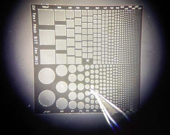
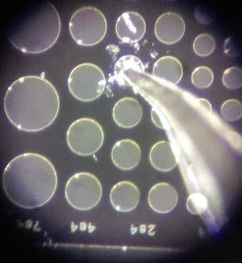
17 Capacitors Following process flow listed on slide 7: Well dope followed by well-drive anneal, RCA clean 3 Levels of Oxide grown (38Å, 52Å, 68Å, 1 wafer each) Nitride deposited (~75Å All) with Device wafers Alumina (~110Å All) deposited with device wafers TaN (2500Å All) deposited as per Film Optimization Aluminum (~5000Å All) deposited with CHA Flash Evaporator. GCA C-V Mask patterned, Aluminum wet etched, and TaN etched with Drytech Quad. Wet photoresist strip (PRS2000) performed, rather than O 2 plasma ash, to avoid formation of Ta 2 O 5 after etch. 17
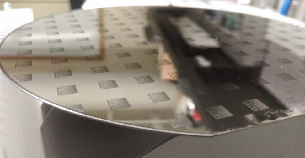
18 Capacitors 18
19 Capacitors 19
20 Capacitors 20
21 Further Work Device Wafer Completion Once the device wafers have completed the process flow outlined in slide 7, they should prove fully functional Threshold voltage adjustment by hot carrier injection should be achievable, based on the good results seen with C-V wafers Theoretical scaling limits can then likely be extracted from these results. 21
22 Special Thanks to: Dr. Santosh Kurinec Dr. Michael Jackson ****The SMFL Staff!!!*** Matt Filmer, Nick Edwards Dr. Robert Pearson and Dr. Ewbank
23 Questions?
Amorphous Carbon Hard Mask for Multiple Patterning Lithography
 Amorphous Carbon Hard Mask for Multiple Patterning Lithography TIMOTHY D. HORN 33 RD ANNUAL MICROELECTRONIC ENGINEERING CONFERENCE RIT MICROELECTRONIC ENGINEERING Outline I. Background carbon hard mask
Summary of Selected EMCR732 Projects for Spring 2005 Mike Aquilino Dr. Lynn Fuller
 ROCHESTER INSTITUTE OF TECHNOLOGY MICROELECTRONIC ENGINEERING Summary of Selected EMCR732 Projects for Spring 2005 Mike Aquilino Dr. Lynn Fuller Motorola Professor 82 Lomb Memorial Drive Rochester, NY
3.155J / 6.152J Micro/Nano Processing Technology TAKE-HOME QUIZ FALL TERM 2005
 3.155J / 6.152J Micro/Nano Processing Technology TAKE-HOME QUIZ FALL TERM 2005 1) This is an open book, take-home quiz. You are not to consult with other class members or anyone else. You may discuss the
Fabrication Process. Crystal Growth Doping Deposition Patterning Lithography Oxidation Ion Implementation CONCORDIA VLSI DESIGN LAB
 Fabrication Process Crystal Growth Doping Deposition Patterning Lithography Oxidation Ion Implementation 1 Fabrication- CMOS Process Starting Material Preparation 1. Produce Metallurgical Grade Silicon
The Physical Structure (NMOS)
") The Physical Structure (NMOS) Al SiO2 Field Oxide Gate oxide S n+ Polysilicon Gate Al SiO2 SiO2 D n+ L channel P Substrate Field Oxide contact Metal (S) n+ (G) L W n+ (D) Poly 1 3D Perspective 2 3 Fabrication
The Physical Structure (NMOS) Al SiO2 Field Oxide Gate oxide S n+ Polysilicon Gate Al SiO2 SiO2 D n+ L channel P Substrate Field Oxide contact Metal (S) n+ (G) L W n+ (D) Poly 1 3D Perspective 2 3 Fabrication
3.155J / 6.152J MICROELECTRONICS PROCESSING TECHNOLOGY TAKE-HOME QUIZ FALL TERM 2003
 3.155J / 6.152J MICROELECTRONICS PROCESSING TECHNOLOGY TAKE-HOME QUIZ FALL TERM 2003 1) This is an open book, take-home quiz. You are not to consult with other class members or anyone else. You may discuss
EE 330 Lecture 8. IC Fabrication Technology Part II. - Oxidation - Epitaxy - Polysilicon - Interconnects
 EE 330 Lecture 8 IC Fabrication Technology Part II - Oxidation - Epitaxy - Polysilicon - Interconnects Review from Last Time MOS Transistor Bulk Source Gate Drain p-channel MOSFET Lightly-doped n-type
MEMS Surface Fabrication
 ROCHESTER INSTITUTE OF TECHNOLOGY MICROELECTRONIC ENGINEERING MEMS Surface Fabrication Dr. Lynn Fuller webpage: http://people.rit.edu/lffeee Electrical and Microelectronic Engineering Rochester Institute
VLSI INTRODUCTION P.VIDYA SAGAR ( ASSOCIATE PROFESSOR) Department of Electronics and Communication Engineering, VBIT
 Department of Electronics and Communication Engineering, VBIT") VLSI INTRODUCTION P.VIDYA SAGAR ( ASSOCIATE PROFESSOR) contents UNIT I INTRODUCTION: Introduction to IC Technology MOS, PMOS, NMOS, CMOS & BiCMOS technologies. BASIC ELECTRICAL PROPERTIES : Basic Electrical
VLSI INTRODUCTION P.VIDYA SAGAR ( ASSOCIATE PROFESSOR) contents UNIT I INTRODUCTION: Introduction to IC Technology MOS, PMOS, NMOS, CMOS & BiCMOS technologies. BASIC ELECTRICAL PROPERTIES : Basic Electrical
EE 330 Lecture 9. IC Fabrication Technology Part II. -Oxidation -Epitaxy -Polysilicon -Planarization -Resistance and Capacitance in Interconnects
 EE 330 Lecture 9 IC Fabrication Technology Part II -Oxidation -Epitaxy -Polysilicon -Planarization -Resistance and Capacitance in Interconnects Review from Last Time IC Fabrication Technology Crystal Preparation
VLSI Technology. By: Ajay Kumar Gautam
 By: Ajay Kumar Gautam Introduction to VLSI Technology, Crystal Growth, Oxidation, Epitaxial Process, Diffusion Process, Ion Implantation, Lithography, Etching, Metallization, VLSI Process Integration,
Introduction to CMOS VLSI Design. Layout, Fabrication, and Elementary Logic Design
 Introduction to CMOS VLSI Design Layout, Fabrication, and Elementary Logic Design CMOS Fabrication CMOS transistors are fabricated on silicon wafer Lithography process similar to printing press On each
EECS130 Integrated Circuit Devices
 EECS130 Integrated Circuit Devices Professor Ali Javey 9/13/2007 Fabrication Technology Lecture 1 Silicon Device Fabrication Technology Over 10 15 transistors (or 100,000 for every person in the world)
Chapter 3 Silicon Device Fabrication Technology
 Chapter 3 Silicon Device Fabrication Technology Over 10 15 transistors (or 100,000 for every person in the world) are manufactured every year. VLSI (Very Large Scale Integration) ULSI (Ultra Large Scale
Summary of Selected EMCR650/731 Projects for Jeremiah Hebding Dr. Lynn Fuller
 ROCHESTER INSTITUTE OF TECHNOLOGY MICROELECTRONIC ENGINEERING Summary of Selected EMCR650/731 Projects for 2004-2005 Jeremiah Hebding Dr. Lynn Fuller Motorola Professor 82 Lomb Memorial Drive Rochester,
Chapter 4. UEEP2613 Microelectronic Fabrication. Oxidation
 Chapter 4 UEEP2613 Microelectronic Fabrication Oxidation Prepared by Dr. Lim Soo King 24 Jun 2012 Chapter 4...113 Oxidation...113 4.0 Introduction... 113 4.1 Chemistry of Silicon Dioxide Formation... 115
Resistive Transition Metal Oxide Memory
 Resistive Transition Metal Oxide Memory Senior Project Microelectronic Engineering Wilkie Olin-Ammentorp, Microelectronic Engineering Advisor: Santosh Kurinec 5/11/2015 Introduction to Memory Many different
Schematic creation of MOS field effect transistor.
 Schematic creation of MOS field effect transistor. Gate electrode Drain electrode Source electrode Gate oxide Gate length Page 1 Step 0 The positively doped silicon wafer is first coated with an insulating
6.777J/2.732J Design and Fabrication of Microelectromechanical Devices Spring Term Solution to Problem Set 2 (16 pts)
") 6.777J/2.732J Design and Fabrication of Microelectromechanical Devices Spring Term 2007 By Brian Taff (Adapted from work by Feras Eid) Solution to Problem Set 2 (16 pts) Issued: Lecture 4 Due: Lecture
6.777J/2.732J Design and Fabrication of Microelectromechanical Devices Spring Term 2007 By Brian Taff (Adapted from work by Feras Eid) Solution to Problem Set 2 (16 pts) Issued: Lecture 4 Due: Lecture
CMOS Fabrication. Dr. Bassam Jamil. Adopted from slides of the textbook
 CMOS Fabrication Dr. Bassam Jamil Adopted from slides of the textbook CMOS Fabrication CMOS transistors are fabricated on silicon wafer Lithography process similar to printing press On each step, different
Chapter 2 Manufacturing Process
 Digital Integrated Circuits A Design Perspective Chapter 2 Manufacturing Process 1 CMOS Process 2 CMOS Process (n-well) Both NMOS and PMOS must be built in the same silicon material. PMOS in n-well NMOS
Highly Reliable Low Temperature Ultrathin Oxides Grown Using N 2 O Plasma
 Highly Reliable Low Temperature Ultrathin Oxides Grown Using N 2 O Plasma Jam-Wem Lee 1, Yiming Li 1,2, and S. M. Sze 1,3 1 Department of Nano Device Technology, National Nano Device Laboratories, Hsinchu,
Lecture 1A: Manufacturing& Layout
 Introduction to CMOS VLSI Design Lecture 1A: Manufacturing& Layout David Harris Harvey Mudd College Spring 2004 Steven Levitan Fall 2008 1 The Manufacturing Process For a great tour through the IC manufacturing
This Appendix discusses the main IC fabrication processes.
 IC Fabrication B B.1 Introduction This Appendix discusses the main IC fabrication processes. B.2 NMOS fabrication NMOS transistors are formed in a p-type substrate. The NMOS fabrication process requires
Plasma-Enhanced Chemical Vapor Deposition
 Plasma-Enhanced Chemical Vapor Deposition Steven Glenn July 8, 2009 Thin Films Lab 4 ABSTRACT The objective of this lab was to explore lab and the Applied Materials P5000 from a different point of view.
Physical Vapor Deposition (PVD) Zheng Yang
 Zheng Yang") Physical Vapor Deposition (PVD) Zheng Yang ERF 3017, email: yangzhen@uic.edu Page 1 Major Fabrication Steps in MOS Process Flow UV light Mask oxygen Silicon dioxide photoresist exposed photoresist oxide
Physical Vapor Deposition (PVD) Zheng Yang ERF 3017, email: yangzhen@uic.edu Page 1 Major Fabrication Steps in MOS Process Flow UV light Mask oxygen Silicon dioxide photoresist exposed photoresist oxide
FABRICATION of MOSFETs
 FABRICATION of MOSFETs CMOS fabrication sequence -p-type silicon substrate wafer -creation of n-well regions for pmos transistors, -impurity implantation into the substrate. -thick oxide is grown in the
EE40 Lec 22. IC Fabrication Technology. Prof. Nathan Cheung 11/19/2009
 Suggested Reading EE40 Lec 22 IC Fabrication Technology Prof. Nathan Cheung 11/19/2009 300mm Fab Tour http://www-03.ibm.com/technology/manufacturing/technology_tour_300mm_foundry.html Overview of IC Technology
Brian Izzio 5th Year Microelectronic Engineering Student. Rochester Institute of Technology
 CAPACITAWZE-VOI~TAGE characterization FOR POLYSILICON GATE MOS CAPACITORS DJTRODUcTION Brian Izzio 5th Year Microelectronic Engineering Student Rochester Institute of Technology ABSTRACT The effects of
ECE 440 Lecture 27 : Equilibrium P-N Junctions I Class Outline:
 ECE 440 Lecture 27 : Equilibrium P-N Junctions I Class Outline: Fabrication of p-n junctions Contact Potential Things you should know when you leave Key Questions What are the necessary steps to fabricate
Today s Class. Materials for MEMS
 Lecture 2: VLSI-based Fabrication for MEMS: Fundamentals Prasanna S. Gandhi Assistant Professor, Department of Mechanical Engineering, Indian Institute of Technology, Bombay, Recap: Last Class What is
Czochralski Crystal Growth
 Czochralski Crystal Growth Crystal Pulling Crystal Ingots Shaping and Polishing 300 mm wafer 1 2 Advantage of larger diameter wafers Wafer area larger Chip area larger 3 4 Large-Diameter Wafer Handling
Etching Etching Definitions Isotropic Etching: same in all direction Anisotropic Etching: direction sensitive Selectivity: etch rate difference
 Etching Etching Definitions Isotropic Etching: same in all direction Anisotropic Etching: direction sensitive Selectivity: etch rate difference between 2 materials Need strong selectivity from masking
EE 330 Lecture 9. IC Fabrication Technology Part 2
 EE 330 Lecture 9 IC Fabrication Technology Part 2 Quiz 8 A 2m silicon crystal is cut into wafers using a wire saw. If the wire diameter is 220um and the wafer thickness is 350um, how many wafers will this
EE 330 Lecture 9. IC Fabrication Technology Part II. -Oxidation -Epitaxy -Polysilicon -Planarization -Resistance and Capacitance in Interconnects
 EE 330 Lecture 9 IC Fabrication Technology Part II -Oxidation -Epitaxy -Polysilicon -Planarization -Resistance and Capacitance in Interconnects Review from Last Time Etching Dry etch (anisotropic) SiO
EE 434 Lecture 9. IC Fabrication Technology
 EE 434 Lecture 9 IC Fabrication Technology Quiz 7 The layout of a film resistor with electrodes A and B is shown. If the sheet resistance of the film is 40 /, determine the resistance between nodes A and
Chapter 3 CMOS processing technology
 Chapter 3 CMOS processing technology (How to make a CMOS?) Si + impurity acceptors(p-type) donors (n-type) p-type + n-type => pn junction (I-V) 3.1.1 (Wafer) Wafer = A disk of silicon (0.25 mm - 1 mm thick),
Chemical Vapor Deposition
 Chemical Vapor Deposition ESS4810 Lecture Fall 2010 Introduction Chemical vapor deposition (CVD) forms thin films on the surface of a substrate by thermal decomposition and/or reaction of gas compounds
Lecture 0: Introduction
 Lecture 0: Introduction Introduction Integrated circuits: many transistors on one chip. Very Large Scale Integration (VLSI): bucketloads! Complementary Metal Oxide Semiconductor Fast, cheap, low power
Lect. 2: Basics of Si Technology
 Unit processes Thin Film Deposition Etching Ion Implantation Photolithography Chemical Mechanical Polishing 1. Thin Film Deposition Layer of materials ranging from fractions of nanometer to several micro-meters
CMP Process Development for Shallow Trench Isolation (STI)
") CMP Process Development for Shallow Trench Isolation (STI) Robert A. Seifridge Microelectronic Engineering Rochester Institute of Technology Rochester, NY 14623 Abstract Tool characterization and optimization
CMP Process Development for Shallow Trench Isolation (STI) Robert A. Seifridge Microelectronic Engineering Rochester Institute of Technology Rochester, NY 14623 Abstract Tool characterization and optimization
Process Integration. NMOS Generic NMOS Process Flow. CMOS - The MOSIS Process Flow
 Process Integration Self-aligned Techniques LOCOS- self-aligned channel stop Self-aligned Source/Drain Lightly Doped Drain (LDD) Self-aligned silicide (SALICIDE) Self-aligned oxide gap MEMS Release Techniques
Technology. Semiconductor Manufacturing. Hong Xiao INTRODUCTION TO SECOND EDITION SPIE PRESS
 INTRODUCTION TO Semiconductor Manufacturing Technology SECOND EDITION Hong Xiao TECHNISCHE INFORMATIONSBiBUOTHEK UNIVERSITATSBIBLIOTHEK HANNOVER SPIE PRESS Bellingham,Washington USA Contents Preface to
Bulk MEMS Fabrication Details Dr. Lynn Fuller, Casey Gonta, Patsy Cadareanu
 ROCHESTER INSTITUTE OF TECHNOLOGY MICROELECTRONIC ENGINEERING Bulk MEMS Fabrication Details Dr. Lynn Fuller, Casey Gonta, Patsy Cadareanu Webpage: http://people.rit.edu/lffeee 82 Lomb Memorial Drive Rochester,
Isolation Technology. Dr. Lynn Fuller
 ROCHESTER INSTITUTE OF TECHNOLOGY MICROELECTRONIC ENGINEERING Isolation Technology Dr. Lynn Fuller Motorola Professor 82 Lomb Memorial Drive Rochester, NY 14623-5604 Tel (585) 475-2035 Fax (585) 475-5041
CMOS FABRICATION. n WELL PROCESS
 CMOS FABRICATION n WELL PROCESS Step 1: Si Substrate Start with p- type substrate p substrate Step 2: Oxidation Exposing to high-purity oxygen and hydrogen at approx. 1000 o C in oxidation furnace SiO
Doping and Oxidation
 Technische Universität Graz Institute of Solid State Physics Doping and Oxidation Franssila: Chapters 13,14, 15 Peter Hadley Technische Universität Graz Institute of Solid State Physics Doping Add donors
Make sure the exam paper has 9 pages total (including cover page)
") UNIVERSITY OF CALIFORNIA College of Engineering Department of Electrical Engineering and Computer Sciences Fall 2010 EE143 Midterm Exam #2 Family Name First name SID Signature Solution Make sure the exam
UNIVERSITY OF CALIFORNIA College of Engineering Department of Electrical Engineering and Computer Sciences Fall 2010 EE143 Midterm Exam #2 Family Name First name SID Signature Solution Make sure the exam
Microelectronic Device Instructional Laboratory. Table of Contents
 Introduction Process Overview Microelectronic Device Instructional Laboratory Introduction Description Flowchart MOSFET Development Process Description Process Steps Cleaning Solvent Cleaning Photo Lithography
Lecture Day 2 Deposition
 Deposition Lecture Day 2 Deposition PVD - Physical Vapor Deposition E-beam Evaporation Thermal Evaporation (wire feed vs boat) Sputtering CVD - Chemical Vapor Deposition PECVD LPCVD MVD ALD MBE Plating
CS/ECE 5710/6710. N-type Transistor. N-type from the top. Diffusion Mask. Polysilicon Mask. CMOS Processing
 CS/ECE 5710/6710 CMOS Processing Addison-Wesley N-type Transistor D G +Vgs + Vds S N-type from the top i electrons - Diffusion Mask Mask for just the diffused regions Top view shows patterns that make
Process Improvement Projects May 2006 Dr. Lynn Fuller
 ROCHESTER INSTITUTE OF TECHNOLOGY MICROELECTRONIC ENGINEERING Process Improvement Projects May 2006 Dr. Lynn Fuller 82 Lomb Memorial Drive Rochester, NY 14623-5604 Tel (585) 475-2035 Fax (585) 475-5041
Process Integration. MEMS Release Techniques Sacrificial Layer Removal Substrate Undercut
 Process Integration Self-aligned Techniques LOCOS- self-aligned channel stop Self-aligned Source/Drain Lightly Doped Drain (LDD) Self-aligned silicide (SALICIDE) Self-aligned oxide gap MEMS Release Techniques
PROCESS FLOW AN INSIGHT INTO CMOS FABRICATION PROCESS
 Contents: VI Sem ECE 06EC63: Analog and Mixed Mode VLSI Design PROCESS FLOW AN INSIGHT INTO CMOS FABRICATION PROCESS 1. Introduction 2. CMOS Fabrication 3. Simplified View of Fabrication Process 3.1 Alternative
Review of CMOS Processing Technology
 - Scaling and Integration Moore s Law Unit processes Thin Film Deposition Etching Ion Implantation Photolithography Chemical Mechanical Polishing 1. Thin Film Deposition Layer of materials ranging from
UT Austin, ECE Department VLSI Design 2. CMOS Fabrication, Layout Rules
 2. CMOS Fabrication, Layout, Design Rules Last module: Introduction to the course How a transistor works CMOS transistors This module: CMOS Fabrication Design Rules CMOS Fabrication CMOS transistors are
Process Flow in Cross Sections
 Process Flow in Cross Sections Process (simplified) 0. Clean wafer in nasty acids (HF, HNO 3, H 2 SO 4,...) --> wear gloves! 1. Grow 500 nm of SiO 2 (by putting the wafer in a furnace with O 2 2. Coat
EE C245 ME C218 Introduction to MEMS Design Fall 2011
 Lecture Outline EE C245 ME C218 Introduction to MEMS Design Fall 2011 Prof. Clark T.-C. Nguyen Dept. of Electrical Engineering & Computer Sciences University of California at Berkeley Berkeley, CA 94720
VLSI. Lecture 1. Jaeyong Chung System-on-Chips (SoC) Laboratory Incheon National University. Based on slides of David Money Harris
 Laboratory Incheon National University. Based on slides of David Money Harris") VLSI Lecture 1 Jaeyong Chung System-on-Chips (SoC) Laboratory Incheon National University Based on slides of David Money Harris Goals of This Course Learn the principles of VLSI design Learn to design
VLSI Lecture 1 Jaeyong Chung System-on-Chips (SoC) Laboratory Incheon National University Based on slides of David Money Harris Goals of This Course Learn the principles of VLSI design Learn to design
conductor - gate insulator source gate n substrate conductor - gate insulator gate substrate n open switch closed switch however: closed however:
 MOS Transistors Readings: Chapter 1 N-type drain conductor - gate insulator source gate drain source n p n substrate P-type drain conductor - gate insulator source drain gate source p p substrate n 42
5.8 Diaphragm Uniaxial Optical Accelerometer
 5.8 Diaphragm Uniaxial Optical Accelerometer Optical accelerometers are based on the BESOI (Bond and Etch back Silicon On Insulator) wafers, supplied by Shin-Etsu with (100) orientation, 4 diameter and
CMOS VLSI Design. Introduction. All materials are from the textbook Weste and Harris, 3 rd Edition CMOS VLSI DESIGN. Introduction
 CMOS VLSI Design Introduction ll materials are from the textbook Weste and Harris, 3 rd Edition CMOS VLSI DESIGN Introduction Chapter previews the entire field, subsequent chapters elaborate on specific
Process Development of Sidewall Spacer Features for Sub-300nm Dense Silicon FinFETs
 35 th Annual Microelectronic Engineering Conference, May 2017 1 Process Development of Sidewall Spacer Features for Sub-300nm Dense Silicon FinFETs Salwan Omar MCEE Microelectronics Engineering Rochester,
Thermal Oxidation and Growth of Insulators (Chapter 3 - Jaeger 3) Key advantage of Si: Oxidation of Si into SiO 2 (glass) Major factor in making
 Key advantage of Si: Oxidation of Si into SiO 2 (glass) Major factor in making") Thermal Oxidation and Growth of Insulators (Chapter 3 - Jaeger 3) Key advantage of Si: Oxidation of Si into SiO (glass) Major factor in making Silicon the main semiconductor Grown at high temperature in
Thermal Oxidation and Growth of Insulators (Chapter 3 - Jaeger 3) Key advantage of Si: Oxidation of Si into SiO (glass) Major factor in making Silicon the main semiconductor Grown at high temperature in
CMOS Factory Laboratory
 ROCHESTER INSTITUTE OF TECHNOLOGY MICROELECTRONIC ENGINEERING CMOS Factory Laboratory Dr. Lynn Fuller Webpage: http://people.rit.edu/lffeee 82 Lomb Memorial Drive Rochester, NY 14623-5604 Tel (585) 475-2035
LAM 490 Etch Recipes. Dr. Lynn Fuller
 ROCHESTER INSTITUTE OF TECHNOLOGY MICROELECTRONIC ENGINEERING LAM 490 Etch Recipes Dr. Lynn Fuller Professor, Webpage: http://people.rit.edu/lffeee 82 Lomb Memorial Drive Rochester, NY 14623-5604 Tel (585)
Department of Electrical Engineering. Jungli, Taiwan
 Chapter 3 Fabrication of CMOS Integrated Circuits Jin-Fu Li Department of Electrical Engineering National Central University Jungli, Taiwan Background Outline The CMOS Process Flow Design Rules Latchup
EE 143 FINAL EXAM NAME C. Nguyen May 10, Signature:
 INSTRUCTIONS Read all of the instructions and all of the questions before beginning the exam. There are 5 problems on this Final Exam, totaling 143 points. The tentative credit for each part is given to
Lecture #18 Fabrication OUTLINE
 Transistors on a Chip Lecture #18 Fabrication OUTLINE IC Fabrication Technology Introduction the task at hand Doping Oxidation Thin-film deposition Lithography Etch Lithography trends Plasma processing
Fairchild Semiconductor Application Note June 1983 Revised March 2003
 Fairchild Semiconductor Application Note June 1983 Revised March 2003 High-Speed CMOS (MM74HC) Processing The MM74HC logic family achieves its high speed by utilizing microcmos Technology. This is a 3.5
Chapter 3. In this chapter, we use sol-gel method to combine three high-k precursors, i.e. HfCl 4, ZrCl 4 and SiCl 4 together to form hafnium silicate
 Chapter 3 Sol-Gel-Derived Zirconium Silicate (ZrSi x O y ) and Hafnium Silicate (HfSi x O y ) Co-existed Nanocrystal SONOS Memory 3-1 Introduction In the previous chapter, we fabricate the sol-gel-derived
2015 EE410-LOCOS 0.5µm Poly CMOS Process Run Card Lot ID:
 STEP 0.00 - PHOTOMASK #0- ZERO LEVEL MARKS Starting materials is n-type silicon (5-10 ohm-cm). Add four test wafers labeled T1-T4. T1 and T2 will travel with the device wafers and get all of the processing
MATTHEW A. WICKHAM 5th Year Microelectronic Engineering Student Rochester Institute of Technology ABSTRACT
 ION IMPLANTATION TO ADJUST NMOS THRESHOLD VOLTAGES MATTHEW A. WICKHAM 5th Year Microelectronic Engineering Student Rochester Institute of Technology INTRODUCTION ABSTRACT NMOS processes require a variety
Cobalt Silicide Formation and Patterning Technology
 Cobalt Silicide Formation and Patterning Technology Neil S. Patel Microelectronic Engineering Rochester Institute of Technology Rochester, NY 14623 Abstract The goal of this investigation was to develop
Examples of dry etching and plasma deposition at Glasgow University
 Examples of dry etching and plasma deposition at Glasgow University Glasgow has pioneered and established many novel research activities involving the development of new dry etch processes and dry etch
PHYS 534 (Fall 2008) Process Integration OUTLINE. Examples of PROCESS FLOW SEQUENCES. >Surface-Micromachined Beam
 Process Integration OUTLINE. Examples of PROCESS FLOW SEQUENCES. >Surface-Micromachined Beam") PHYS 534 (Fall 2008) Process Integration Srikar Vengallatore, McGill University 1 OUTLINE Examples of PROCESS FLOW SEQUENCES >Semiconductor diode >Surface-Micromachined Beam Critical Issues in Process
PHYS 534 (Fall 2008) Process Integration Srikar Vengallatore, McGill University 1 OUTLINE Examples of PROCESS FLOW SEQUENCES >Semiconductor diode >Surface-Micromachined Beam Critical Issues in Process
2-1 Introduction The demand for high-density, low-cost, low-power consumption,
 Chapter 2 Hafnium Silicate (HfSi x O y ) Nanocrystal SONOS-Type Flash Memory Fabricated by Sol-Gel Spin Coating Method Using HfCl 4 and SiCl 4 as Precursors 2-1 Introduction The demand for high-density,
LAM4600 Plasma Etch Tool Recipes Dr. Lynn Fuller Webpage:
 ROCHESTER INSTITUTE OF TECHNOLOGY MICROELECTRONIC ENGINEERING LAM4600 Plasma Etch Tool Recipes Webpage: http://people.rit.edu/lffeee 82 Lomb Memorial Drive Rochester, NY 14623-5604 Tel (585) 475-2035 Email:
Total Points = 110 possible (graded out of 100)
") Lab Report 1 Table of Contents 1. Profiles & Layout (9 Points) 2. Process Procedures (20 points) 3. Calculations (36 Points) 4. Questions (35 Points) 5. Bonus Questions (10 Points) Total Points = 110 possible
Lab Report 1 Table of Contents 1. Profiles & Layout (9 Points) 2. Process Procedures (20 points) 3. Calculations (36 Points) 4. Questions (35 Points) 5. Bonus Questions (10 Points) Total Points = 110 possible
IC/MEMS Fabrication - Outline. Fabrication
 IC/MEMS Fabrication - Outline Fabrication overview Materials Wafer fabrication The Cycle: Deposition Lithography Etching Fabrication IC Fabrication Deposition Spin Casting PVD physical vapor deposition
Fabrication and Layout
 ECEN454 Digital Integrated Circuit Design Fabrication and Layout ECEN 454 3.1 A Glimpse at MOS Device Polysilicon Aluminum ECEN 475 4.2 1 Material Classification Insulators Glass, diamond, silicon oxide
Ajay Kumar Gautam [VLSI TECHNOLOGY] VLSI Technology for 3RD Year ECE/EEE Uttarakhand Technical University
![Ajay Kumar Gautam [VLSI TECHNOLOGY] VLSI Technology for 3RD Year ECE/EEE Uttarakhand Technical University](/thumbs/75/72824557.jpg "Ajay Kumar Gautam [VLSI TECHNOLOGY] VLSI Technology for 3RD Year ECE/EEE Uttarakhand Technical University") 2014 Ajay Kumar Gautam [VLSI TECHNOLOGY] VLSI Technology for 3RD Year ECE/EEE Uttarakhand Technical University Page1 Syllabus UNIT 1 Introduction to VLSI Technology: Classification of ICs, Scale of integration,
2014 Ajay Kumar Gautam [VLSI TECHNOLOGY] VLSI Technology for 3RD Year ECE/EEE Uttarakhand Technical University Page1 Syllabus UNIT 1 Introduction to VLSI Technology: Classification of ICs, Scale of integration,
CMOS Technology. Flow varies with process types & company. Start with substrate selection. N-Well CMOS Twin-Well CMOS STI
 CMOS Technology Flow varies with process types & company N-Well CMOS Twin-Well CMOS STI Start with substrate selection Type: n or p Doping level, resistivity Orientation, 100, or 101, etc Other parameters
Figure 2.3 (cont., p. 60) (e) Block diagram of Pentium 4 processor with 42 million transistors (2000). [Courtesy Intel Corporation.
 (e) Block diagram of Pentium 4 processor with 42 million transistors (2000). [Courtesy Intel Corporation.") Figure 2.1 (p. 58) Basic fabrication steps in the silicon planar process: (a) oxide formation, (b) selective oxide removal, (c) deposition of dopant atoms on wafer, (d) diffusion of dopant atoms into exposed
Figure 2.1 (p. 58) Basic fabrication steps in the silicon planar process: (a) oxide formation, (b) selective oxide removal, (c) deposition of dopant atoms on wafer, (d) diffusion of dopant atoms into exposed
PRELIMINARY FORMATION OF DEEP TRENCH C~P~CITORS
 PRELIMINARY FORMATION OF DEEP TRENCH C~P~CITORS Christopher 3. Waskiewicz 5th Year Microelectronic Engineering Student Rochester Institute of Technology ABSTRACT ~ Tegal 700 plasma etcher was used to etch
ALD of Scandium Oxide from Tris(N,N -diisopropylacetamidinato)scandium and Water
scandium and Water") ALD of Scandium Oxide from Tris(N,N -diisopropylacetamidinato)scandium and Water Philippe P. de Rouffignac, Roy G. Gordon Dept. of Chemistry,, Cambridge, MA gordon@chemistry.harvard.edu (617) 495-4017
ALD of Scandium Oxide from Tris(N,N -diisopropylacetamidinato)scandium and Water Philippe P. de Rouffignac, Roy G. Gordon Dept. of Chemistry,, Cambridge, MA gordon@chemistry.harvard.edu (617) 495-4017
Chapter 2 Problems. The CMOS technology we need to realize is shown below, from Figure 1-34 in the text. S P + N P + N WELL P +
 Chapter 2 roblems 2.1 Sketch a process flow that would result in the structure shown in Figure 1-34 by drawing a series of drawings similar to those in this chapter. You only need to describe the flow
NMOS Transistor Design and Fabrication for S-Parameter Extraction
 James, A.L. 23 ~ Annual Microelectronic Engineering Conference. May 25 NMOS Transistor Design and Fabrication for S-Parameter Extraction Adam L. James, Student Member, IEEE,4 bstrad A successful test layout
FABRICATION OF CMOS INTEGRATED CIRCUITS. Dr. Mohammed M. Farag
 FABRICATION OF CMOS INTEGRATED CIRCUITS Dr. Mohammed M. Farag Outline Overview of CMOS Fabrication Processes The CMOS Fabrication Process Flow Design Rules EE 432 VLSI Modeling and Design 2 CMOS Fabrication
Plasma Etching Rates & Gases Gas ratios affects etch rate & etch ratios to resist/substrate
 Plasma Etching Rates & Gases Gas ratios affects etch rate & etch ratios to resist/substrate Development of Sidewalls Passivating Films Sidewalls get inert species deposited on them with plasma etch Creates
LAM4600 Plasma Etch Tool Recipes Dr. Lynn Fuller
 ROCHESTER INSTITUTE OF TECHNOLOGY MICROELECTRONIC ENGINEERING LAM4600 Plasma Etch Tool Recipes Dr. Lynn Fuller Webpage: http://people.rit.edu/lffeee 82 Lomb Memorial Drive Rochester, NY 14623-5604 Tel
Surface micromachining and Process flow part 1
 Surface micromachining and Process flow part 1 Identify the basic steps of a generic surface micromachining process Identify the critical requirements needed to create a MEMS using surface micromachining
INTEGRATED-CIRCUIT TECHNOLOGY
 INTEGRATED-CIRCUIT TECHNOLOGY 0. Silicon crystal growth and wafer preparation 1. Processing Steps 1.1. Photolitography 1.2. Oxidation 1.3. Layer Deposition 1.4. Etching 1.5. Diffusion 1.6 Backend: assembly,
A Novel Low Temperature Self-Aligned Field Induced Drain Polycrystalline Silicon Thin Film Transistor by Using Selective Side-Etching Process
 Chapter 3 A Novel Low Temperature Self-Aligned Field Induced Drain Polycrystalline Silicon Thin Film Transistor by Using Selective Side-Etching Process 3.1 Introduction Low-temperature poly-si (LTPS) TFTs
Overview of Dual Damascene Cu/Low-k Interconnect
 ERC Retreat Stanford: New Chemistries & Tools for scco 2 Processing of Thin Films Overview of Dual Damascene Cu/Low-k Interconnect P. Josh Wolf 1,4 - Program Manager, Interconnect Div. josh.wolf@sematech.org
Rapid Thermal Processing (RTP) Dr. Lynn Fuller
 Dr. Lynn Fuller") ROCHESTER INSTITUTE OF TECHNOLOGY MICROELECTRONIC ENGINEERING Rapid Thermal Processing (RTP) Dr. Lynn Fuller Webpage: http://people.rit.edu/lffeee 82 Lomb Memorial Drive Rochester, NY 14623-5604 Tel (585)
ROCHESTER INSTITUTE OF TECHNOLOGY MICROELECTRONIC ENGINEERING Rapid Thermal Processing (RTP) Dr. Lynn Fuller Webpage: http://people.rit.edu/lffeee 82 Lomb Memorial Drive Rochester, NY 14623-5604 Tel (585)
UNIT 4. By: Ajay Kumar Gautam Asst. Prof. Dev Bhoomi Institute of Technology & Engineering, Dehradun
 UNIT 4 By: Ajay Kumar Gautam Asst. Prof. Dev Bhoomi Institute of Technology & Engineering, Dehradun Syllabus METALLIZATION: Applications and choices, physical vapor deposition, patterning, problem areas.
Surface Micromachining
 Surface Micromachining Micro Actuators, Sensors, Systems Group University of Illinois at Urbana-Champaign Outline Definition of surface micromachining Most common surface micromachining materials - polysilicon
ELEC 3908, Physical Electronics, Lecture 4. Basic Integrated Circuit Processing
 ELEC 3908, Physical Electronics, Lecture 4 Basic Integrated Circuit Processing Lecture Outline Details of the physical structure of devices will be very important in developing models for electrical behavior