A Design for an efficient cylindrical magnetron cathode with rotating magnets and optical emission incorporated
|
|
|
- Imogene Reynolds
- 5 years ago
- Views:
Transcription


1 Patent on, A Design for an efficient cylindrical magnetron cathode with rotating magnets and optical emission incorporated Inventors A. Subrahmanyam, Krishna Valleti IIT Madras, Chennai, INDIA. Shrikanth V Joshi, G.Sundararajan ARCI, Hyderabad, INDIA.
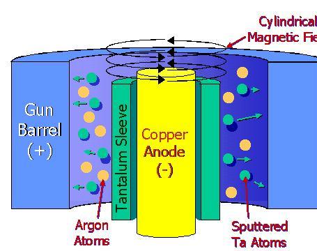
2 Out look of the presentation: Brief introduction to sputtering mechanism Different sputtering techniques focused on planar & cylindrical About & limitations of planar magnetrons (circular, rectangular) Description of existing cylindrical magnetrons Drawbacks Present invention design and evaluation Important references related to present invention


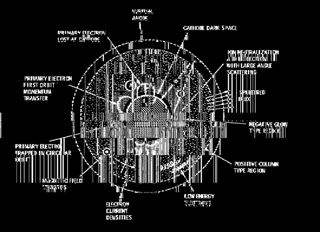
3 Sputtering Process: * Effective creation of Argon ions by secondary electron bombardment
 / B (Gauss) R ion = 911 x E 1/2 (ev) / B (Gauss) Planar magnetron sputtering Cylindrical magnetron sputtering * The magnetic field confines the glow")
4 Sputtering Diode Sputtering Magnetron Sputtering R electron = 3.37 x E 1/2 (ev) / B (Gauss) R ion = 911 x E 1/2 (ev) / B (Gauss) Planar magnetron sputtering Cylindrical magnetron sputtering * The magnetic field confines the glow discharge plasma and increases the length of the path of electrons moving under the influence of the electric field.
5 Planar magnetron sputtering * The cathode includes an array of permanent magnets arranged in a closed loop and mounted in a fixed position in relation to the flat target plate. * The magnetic confinement of the plasma results in a high rate of erosion of the target along the narrow "race track". Limitations * Only a relatively small portion of the total target material is used. * Limited heat transfer and arcing at the edges and the center of the target. * The spitting of debris is very high. * Only planar objects can be coated uniformly.
6
.")

7 Scope of present invention: Batch of Industrial tool coating cost effectively (more number in a single run). For large area glass coatings in the architectural, automotive and display industry. Defense equipment protection form wear and corrosion loss (mainly Gun barrels)


8 Simple Cylindrical magnetron: * Electromagnets requires high current which results in enhanced heating.


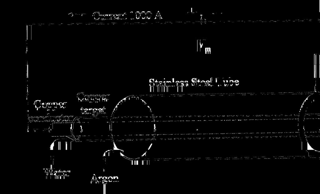
9 Existing Cylindrical magnetron designs: 1 Magnet Non magnetic Spacer U.S.Army Armament Research, Development and Engineering Center * A cathode target assembly in the form of an elongated, cylindrical tube carries a layer of material applied to its outer surface that is to be sputtered. U.S.Army Armament Research, Development and Engineering Center Design reference: US 4,179,351 patent issued on Dec. 18, 1979 to Hawton, Jr. et al.
10 2

11 3 Vacuum coating technologies, Fairfield


12 US 5,047,131 US
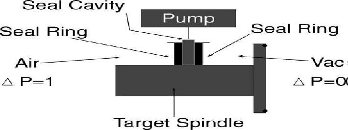
13 * The target tube is rotated about its longitudinal axis. A magnetic structure is arranged inside the tube but does not rotate with it. * The rotation of the target surface through the stationary plasma sputters the top layer of material from entire surface as that surface is rotated through the magnetic field. * Any dielectric that is deposited on the target surface is apparently removed by sputtering when it rotates in the region of the magnetic field thereby reducing arcing ("self-cleaning" ). * The non uniformity in the deposited films is around 12%. * Rotating seals are included in this support structure for isolating the electrical contacts and cooling fluid from the vacuum chamber. * Rotation of the target (not magnetic arrangement) results in local gas fluctuations. * Sputtering in rotating target geometry will not allow oblique deposition (which results in improved depositing film properties). * Permanent magnets were damaged with time because of coolant water circulation (over the magnets) and the magnetic field strength decreases slowly.

 K function of working pressure and")
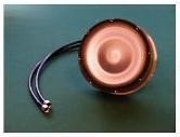
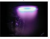
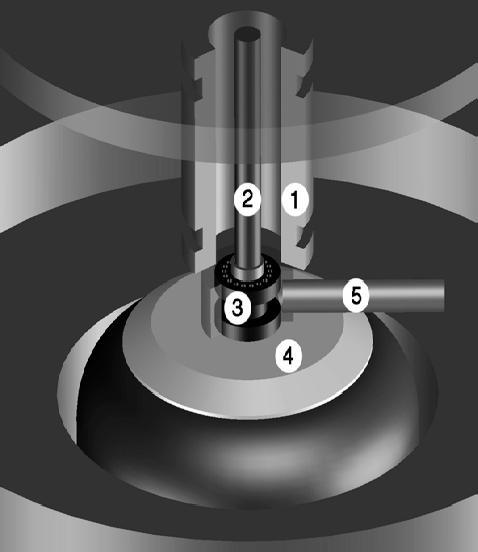
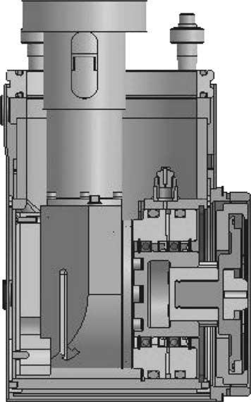
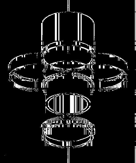
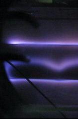
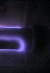
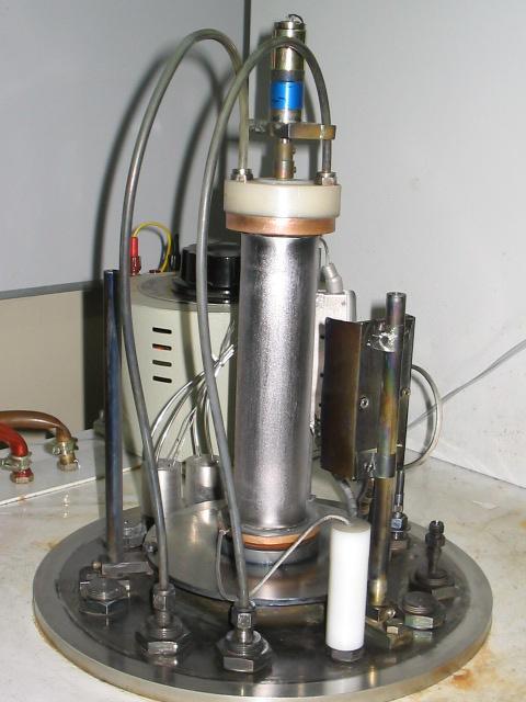
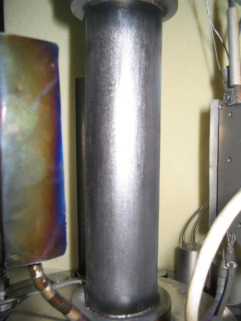
14 Present Invention: Optical fiber port High torque Motor Power connection Cooling water port Magnet arrangement Cylindrical cathode Plasma profile * Electron Confining efficiency; I = K V n, n = 6.8 ( in the present geometry) K function of working pressure and magnetic field strength.
15
16

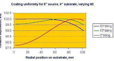
17 Thickness variation along the cylindrical axis: % thickness variation from average value ± 3 % Distance from one end of CM (cm) * A strip 12.0 cm 2.5 cm of glass plate is used as substrate. * Surface profilometry is used for thickness measurements. 10 Surface at the step Target Utilization: U t = t t w w ( initial ) ( final ) 100 % In the present design; U t 90%
18 Process control by plasma emission monitoring: Plasma Emission spectra Argon (first ionization) nm Tantalum (atomic) nm Nitrogen (exited) nm
19 Over all achievements in the design: Maximum uniformity in thickness along the length of the cylindrical magnetron is achieved Maximum target utilization is achieved Complicated rotation seal mechanism is eliminated Permanent magnetic material property degradation by corrosion is eliminated Ease of target loading is achieved Difficulties in monitoring gas distribution uniformity by gas showers is eliminated
20 Important references: 1. Design advances and applications of the rotatable cylindrical magnetron by Michael Wright and Terry Beardow JVST A 4 (1986) Homogeneous coatings inside cylinders by F. Loffler and C. Siewert Surf. Coat. Technol (2004) Characterization and Comparison of Magnetron Sputtered and Electroplated Gun Bore Coatings by Christopher P. Mulligan, Stephen B. Smith and Gregory N. Vigilante Transactions of the ASME 128 (2006) Advanced generation of rotatable magnetron technology for high performance reactive sputtering by S.J. Nadel, P. Greene, J. Rietzel, M. Perata, L. Malaszewski, and R. Hill Thin solid films 502 (2006) 15.
Plasma Quest Limited
 Plasma Quest Limited A Remote Plasma Sputter Process for High Rate Web Coating of Low Temperature Plastic Film with High Quality Thin Film Metals and Insulators Dr. Peter Hockley and Prof. Mike Thwaites,
Gencoa Product Portfolio
 Gencoa offer the following range of products & process technology for the thin film industry developed over the last 20 years Planar Magnetrons Plasma Pre- Treaters Reactive Gas Controllers Gencoa Product
AC Reactive Sputtering with Inverted Cylindrical Magnetrons
 AC Reactive Sputtering with Inverted Cylindrical Magnetrons D.A. Glocker, Isoflux Incorporated, Rush, NY; and V.W. Lindberg and A.R. Woodard, Rochester Institute of Technology, Rochester, NY Key Words:
Large Area Coating for Glazing IOP Vacuum Symposium Daresbury 11 th Feb 2010
 Large Area Coating for Glazing IOP Vacuum Symposium Daresbury 11 th Feb 2010 Off-Line Coatings Technology Group Pilkington European Technology Centre 2 NSG Group Pilkington a member of NSG Group from June
A Basic Introduction to Thin-Film Coatings. From the Experts at VaporTech
 A Basic Introduction to Thin-Film Coatings From the Experts at VaporTech What are thin-film coatings? 2018 Vapor Technologies, Inc. All rights reserved. Thin-film coatings Physical or Chemical Vapor Deposition
Dr. Sabrina Lee and Dr. Rong Wei NDIA Gun and Missile Conference, New Orleans, LA April 21-24, 2008
 Weapon Systems & Technology Directorate US ARMY ARDEC- BENÉT LABS TITLE: PLASMA ENHANCED MAGNETRON TECHNOLOGY FOR DURABLE POLLUTION-FREE COATINGS Dr. Sabrina Lee and Dr. Rong Wei NDIA Gun and Missile Conference,
Maximizing the Potential of Rotatable Magnetron Sputter Sources for Web Coating Applications
 Maximizing the Potential of Rotatable Magnetron Sputter Sources for Web Coating Applications V.Bellido-Gonzalez, Dermot Monaghan, Robert Brown, Alex Azzopardi, Gencoa, Liverpool UK Structure of presentation
VERSATILE DEVICE FOR IN-SITU MULTIPLE COATINGS OF LONG, SMALL DIAMETER TUBES Ady Hershcovitch 1, Michael Blaskiewicz 1, J. Michael Brennan 1, Art
 VERSATILE DEVICE FOR IN-SITU MULTIPLE COATINGS OF LONG, SMALL DIAMETER TUBES Ady Hershcovitch 1, Michael Blaskiewicz 1, J. Michael Brennan 1, Art Custer 2, Mark Erickson 2, Wolfram Fischer 1, Chong-Jer
Metallization deposition and etching. Material mainly taken from Campbell, UCCS
 Metallization deposition and etching Material mainly taken from Campbell, UCCS Application Metallization is back-end processing Metals used are aluminum and copper Mainly involves deposition and etching,
Optimization of the Sputtering Process for Depositing Composite Thin Films
 Journal of the Korean Physical Society, Vol. 40, No. 3, March 2002, pp. 511 515 Optimization of the Sputtering Process for Depositing Composite Thin Films M. Farooq Pakistan Council of Renewable Energy
II. NEG THIN FILM DEPOSITION
 Deposition of Non-Evaporable Getter Thin Films and Vacuum Pumping Performances Ankit Sur Engineering Department, Wayne State University, Detroit, MI 48202 The ERL (Energy Recovery Linac) proposed at Cornell
Managing Anode Effects and Substrate Heating from Rotatable Sputter Targets
 Managing Anode Effects and Substrate Heating from Rotatable Sputter Targets Frank Papa*, Dermot Monaghan**, Victor Bellido- González**, and Alex Azzopardi** *Gencoa Technical & Business Support in US,
Linear Plasma Sources for Surface Modification and Deposition for Large Area Coating
 Linear Plasma Sources for Surface Modification and Deposition for Large Area Coating Dr Tony Williams Gencoa Ltd, UK Victor Bellido-Gonzalez, Dr Dermot Monaghan, Dr Joseph Brindley, Robert Brown SVC 2016,
COOLING EFFECT ENHANCEMENT IN MAGNETRON SPUTTERING SYSTEM
 Fifth International Conference on CFD in the Process Industries CSIRO, Melbourne, Australia 13-15 December 2006 COOLING EFFECT ENHANCEMENT IN MAGNETRON SPUTTERING SYSTEM Jae-Sang BAEK and Youn J. KIM*
Decorative Coatings PVD the bright choice
 a parent company of Decorative Coatings PVD the bright choice kenosistec.com a parent company of Why PVD Coating Best surface properties PVD is still one of the most effective method for modifying and
MAGNION Series Sputter Deposition Systems and Cathodes
 Advancing Plasma-Based Technologies PLASMIONIQUE À l Avant-Garde des Technologies Plasma MAGNION Series Sputter Deposition Systems and Cathodes MAGNION Series of Sputter Deposition systems offer Turnkey
Magnetron Sputter Cathodes planar & rotatable. Linear ion sources. Reactive gas controller & endpoint detector
 GENCOA products cover 3 sputtering related areas Magnetron Sputter Cathodes planar & rotatable Reactive gas controller & endpoint detector Linear ion sources Other activities include on-site process implementation,
Previous Lecture. Vacuum & Plasma systems for. Dry etching
 Previous Lecture Vacuum & Plasma systems for Dry etching Lecture 9: Evaporation & sputtering Objectives From this evaporation lecture you will learn: Evaporator system layout & parts Vapor pressure Crucible
INTRODUCTION OF SYS & System
 Vision 2015 INTRODUCTION OF SYS & System PVD & Ion Beam Irradiator Manufacturing Company isys is committed to building the best January. 2007 1 SYS, based on excellent technology and sufficient equipment
Advanced Gun Barrel Technologies (AGBT) Background and Results. NDIA Joint Armaments Conference, 2010
 Background and Results. NDIA Joint Armaments Conference, 2010") Advanced Gun Barrel Technologies (AGBT) Background and Results NDIA Joint Armaments Conference, 2010 Presented by: Mr. Bill Vezina BAE Systems, Inc. Land & Armaments william.vezina@baesystems.com (763)
Advanced Gun Barrel Technologies (AGBT) Background and Results NDIA Joint Armaments Conference, 2010 Presented by: Mr. Bill Vezina BAE Systems, Inc. Land & Armaments william.vezina@baesystems.com (763)
Comparison of Carbon Coatings Deposited by Different Techniques
 Comparison of Carbon Coatings Deposited by Different Techniques V. Gorokhovsky, K.Coulter, M.Miller, R.Wei, C. Ellis, C.Engel Southwest Research Institute San Antonio, Texas Funded by SwRI: Project No.
Growth Of TiO 2 Films By RF Magnetron Sputtering Studies On The Structural And Optical Properties
 Journal of Multidisciplinary Engineering Science and Technology (JMEST) Growth Of TiO 2 Films By RF Magnetron Sputtering Studies On The Structural And Optical Properties Ahmed K. Abbas 1, Mohammed K. Khalaf
Mass Production of Clear Barriers. Requirements on Vacuum Web Coaters for Quality Assurance. Rainer Ludwig, Applied Films, Alzenau, Germany.
 Mass Production of Clear Barriers Requirements on Vacuum Web Coaters for Quality Assurance Rainer Ludwig, Applied Films, Alzenau, Germany Abstract An increasing number of packages using Transparent Barrier
Thin Films: Sputtering Systems (Jaeger Ch 6 & Ruska Ch 7,) Can deposit any material on any substrate (in principal) Start with pumping down to high
 Can deposit any material on any substrate (in principal) Start with pumping down to high") Thin Films: Sputtering Systems (Jaeger Ch 6 & Ruska Ch 7,) Can deposit any material on any substrate (in principal) Start with pumping down to high vacuum ~10-7 torr Removes residual gases eg oxygen from
Thin Films: Sputtering Systems (Jaeger Ch 6 & Ruska Ch 7,) Can deposit any material on any substrate (in principal) Start with pumping down to high vacuum ~10-7 torr Removes residual gases eg oxygen from
PLASMA FLOW AND PLASMA EXPANSION AROUND 3D OBJECTS IN METAL PLASMA IMMERSION ION IMPLANTATION
 PLASMA FLOW AND PLASMA EXPANSION AROUND 3D OBJECTS IN METAL PLASMA IMMERSION ION IMPLANTATION Darina Manova & Stephan Mändl 1 Motivation 2 Motivation Visualisation of Water Flow from Dynamic Sand Dunes
Advanced Gun Barrel Technologies Program Status
 Advanced Gun Barrel Technologies Program Status Dr. Amir Chaboki United Defense NDA Guns -Ammunition - Rockets - Missiles Conference 28 April 2005 FNC227.ppt - Page 1 Large Caliber Naval Guns MK 45 / Mod.
and cost implications of corrosion, casting a spot light on the need for innovation in pipe coating materials and processes.
 A ccording to the Energy Information Administration s International Energy Outlook for 2006, world oil demand is expected to grow from 80 million barrels per day in 2003 to 98 million barrels per day in
Ion-plasma technologies and equipment
 Ion-plasma technologies and equipment VACUUM ION-PLASMA INSTALLATIONS OF «OPAL» SERIES «Opal» series ion-plasma installations are designed for deposition of low-emission, reflective and toned coatings
Effect of pulsed magnetron sputtering process for the deposition of thin layers of nickel and nickel oxide
 Materials Science-Poland, 36(1), 2018, pp. 69-74 http://www.materialsscience.pwr.wroc.pl/ DOI: 10.1515/msp-2017-0092 Effect of pulsed magnetron sputtering process for the deposition of thin layers of nickel
I. PHYSICAL ELECTRONICS. Prof. W. B. Nottingham L. E. Sprague C. J. Marcinkowski R. Steinberg W. E. Mutter M. Wilkinson A. ELECTRON-EMISSION PROBLEMS
 I. PHYSICAL ELECTRONICS Prof. W. B. Nottingham L. E. Sprague C. J. Marcinkowski R. Steinberg W. E. Mutter M. Wilkinson A. ELECTRON-EMISSION PROBLEMS 1. Work Functions and Electrical Conductivity of Oxide-Coated
High Rate Deposition of Reactive Oxide Coatings by New Plasma Enhanced Chemical Vapor Deposition Source Technology
 General Plasma, Inc. 546 East 25th Street Tucson, Arizona 85713 tel. 520-882-5100 fax. 520-882-5165 High Rate Deposition of Reactive Oxide Coatings by New Plasma Enhanced Chemical Vapor Deposition Source
Fabrication Process. Crystal Growth Doping Deposition Patterning Lithography Oxidation Ion Implementation CONCORDIA VLSI DESIGN LAB
 Fabrication Process Crystal Growth Doping Deposition Patterning Lithography Oxidation Ion Implementation 1 Fabrication- CMOS Process Starting Material Preparation 1. Produce Metallurgical Grade Silicon
Deposition of Al/Cu Multilayer By Double Targets Cylindrical DC Magnetron Sputtering System
 JNS 3 (2013) 443-451 Deposition of Al/Cu Multilayer By Double Targets Cylindrical DC Magnetron Sputtering System P. Balashabadi a,*, Z. Assadollahi a, M. Ghasemi a, H. Bakhtiari a, E. Jafari-Khamse b a
Keywords: Sputter deposition; Reactive deposition; Nitride coatings ABSTRACT
 Reactive Cylindrical Magnetron Deposition of Titanium Nitride and Zirconium Nitride Films D.E. Siegfried and D. Cook, Ion Tech, Inc., Ft. Collins, CO; and D. Glocker, Isoflux, Inc., Rush, NY Keywords:
BAK EVAPORATOR FAMILY
 BAK EVAPORATOR FAMILY THE BAK A NEW GENERATION TAKING THE BEST FROM THE PAST, EXPANDING YOUR HORIZONS FOR THE FUTURE! The BAV 2000 - a production giant 2000 BAK SYSTEMS DELIVERED WORLDWIDE 2 BAK EVAPORATOR
A. Hershcovitch, M. Blaskiewicz, J.M. Brennan, W. Fischer, C-J Liaw, W. Meng, R. Todd Brookhaven National Laboratory, Upton, New York 11973, U.S.A A.
 Novel Device for In-Situ Thick Coatings of Long, Small Diameter Accelerator Vacuum Tubes A. Hershcovitch, M. Blaskiewicz, J.M. Brennan, W. Fischer, C-J Liaw, W. Meng, R. Todd Brookhaven National Laboratory,
Microwave Plasma Processing
 Microwave Plasma Processing MUEGGE GMBH Hochstraße 4-6 64385 Reichelsheim Fon +49 (0) 6164-93 07 11 Fax +49 (0) 6164-93 07 93 info@muegge.de www.muegge.de Microwave Plasma Processing Microwave Plasma Technology:
Thin Films: Sputtering Systems (Jaeger Ch 6 & Ruska Ch 7,) Sputtering: gas plasma transfers atoms from target to substrate Can deposit any material
 Sputtering: gas plasma transfers atoms from target to substrate Can deposit any material") Thin Films: Sputtering Systems (Jaeger Ch 6 & Ruska Ch 7,) Sputtering: gas plasma transfers atoms from target to substrate Can deposit any material on any substrate (in principal) Start with pumping down
Thin Films: Sputtering Systems (Jaeger Ch 6 & Ruska Ch 7,) Sputtering: gas plasma transfers atoms from target to substrate Can deposit any material on any substrate (in principal) Start with pumping down
HiPIMS Deposition of Metal and Oxide Coatings
 HiPIMS Deposition of Metal and Oxide Coatings 1 GT West, 1 PJ Kelly, 1 P Barker, 2 JW Bradley and 2 A Mishra 1. Surface Engineering Group, Manchester Metropolitan University, UK 2. Electrical Engineering
Introduction Sample deposition system Cavity deposition system prototype Surface characterization Beyond niobium
 Genfa Wu Introduction Sample deposition system Cavity deposition system prototype Surface characterization Beyond niobium 1 United We Stand Succeed JLAB ECR thin film collaboration: JLAB: L. Phillips,
Solar Selective Absorber Coating Methods Plasma Processes
 Solar Selective Absorber Coating Methods Plasma Processes Paul Gantenbein & Elimar Frank SPF - Institut für Solartechnik University of Applied Sciences Rapperswil (HSR) Optical properties of a selective
THE INCREASE IN THICKNESS UNIFORMITY OF FILMS OBTAINED BY MAGNETRON SPUTTERING WITH ROTATING SUBSTRATE
 Plasma Physics and Technology 3(3):1 14, 216 Department of Physics, FEE CTU in Prague, 216 THE INCREASE IN THICKNESS UNIFORMITY OF FILMS OBTAINED BY MAGNETRON SPUTTERING WITH ROTATING SUBSTRATE Golosov
Deposition of biaxially aligned YSZ layers by dual unbalanced magnetron sputtering.
 Deposition of biaxially aligned YSZ layers by dual unbalanced magnetron sputtering. S. Mahieu, G. De Winter, R. De Gryse University of Ghent, Department of Solid State Sciences, Krijgslaan 281/S1 9000
New Dual Magnetron Plasma Source Designed For Large Area Substrate Pretreatment and Oxide Film Deposition P. Morse, R. Lovro, M. Rost, and J.
 New Dual Magnetron Plasma Source Designed For Large Area Substrate Pretreatment and Oxide Film Deposition P. Morse, R. Lovro, M. Rost, and J. German, Road Map Source Design Theory of Operation Experimental
CERTESS Carbon Diamond-like-Carbon (DLC) Tribological coatings Extreme Hardness + Very low friction = Exceptional Wear Resistance
 Tribological coatings Extreme Hardness + Very low friction = Exceptional Wear Resistance") www.hefusa.net sales@hefusa.net Carbon Diamond-like-Carbon (DLC) Tribological coatings Extreme Hardness + Very low friction = Exceptional Wear Resistance PVD Coatings Overview Physical Vapor Deposition
www.hefusa.net sales@hefusa.net Carbon Diamond-like-Carbon (DLC) Tribological coatings Extreme Hardness + Very low friction = Exceptional Wear Resistance PVD Coatings Overview Physical Vapor Deposition
ION`X HV ROUND MAGNETRONS INTRODUCTION SPECIFICATIONS OPTIONS ACCESSORIES
 ION`X Rely on quality know-how performance ION`X HV ROUND MAGNETRONS INTRODUCTION SPECIFICATIONS OPTIONS ACCESSORIES ROUND MAGNETRONS UHV MAGNETRONS RECTANGULAR ROUND MAGNETRONS UHV MAGNETRONS RECTANGULAR
NASF SURFACE TECHNOLOGY WHITE PAPERS 83 (1), 7-12 (October 2018) Advances in Decorative PVD Chromium Coatings for Polymer Substrates
, 7-12 (October 2018) Advances in Decorative PVD Chromium Coatings for Polymer Substrates") Advances in Decorative PVD Chromium Coatings for Polymer Substrates A Synopsis * of a Presentation given at SUR/FIN 2018 (Cleveland, Ohio) by Gary Vergason ** Vergason Technology, Inc. Van Etten, New York,
Advances in Decorative PVD Chromium Coatings for Polymer Substrates A Synopsis * of a Presentation given at SUR/FIN 2018 (Cleveland, Ohio) by Gary Vergason ** Vergason Technology, Inc. Van Etten, New York,
MICROCHIP MANUFACTURING by S. Wolf
 MICROCHIP MANUFACTURING by S. Wolf Chapter 22 DRY-ETCHING for ULSI APPLICATIONS 2004 by LATTICE PRESS CHAPTER 22 - CONTENTS Types of Dry-Etching Processes The Physics & Chemistry of Plasma-Etching Etching
EFFECTS OF SURFACE PREPARATION TECHNIQUES ON THE ADHESION OF TANTALUM SPUTTERED COATINGS
 TECHNICAL REPORT ARCCB-TR-03015 EFFECTS OF SURFACE PREPARATION TECHNIQUES ON THE ADHESION OF TANTALUM SPUTTERED COATINGS Aisha Bishop Christopher P. Mulligan NOVEMBER 2003 APPROVED FOR PUBLIC RELEASE;
BAK EVAPORATOR FAMILY
 BAK EVAPORATOR FAMILY THE BAK A NEW GENERATION TAKING THE BEST FROM THE PAST, EXPANDING YOUR HORIZONS FOR THE FUTURE! The BAV 2000 - a production giant 2000 BAK SYSTEMS DELIVERED WORLDWIDE 2 BAK EVAPORATOR
Sputter Coating. Technical Brief
 Sputter Coating Technical Brief Document Number TB-SPUTTER Issue 2 (01/02) Introduction HP000107 Quorum Technologies Ltd main sales office: South Stour Avenue Ashford Kent U.K. Tel: ++44(0) 1233 646332
Energy-efficient glazing
 Energy-efficient glazing Low-E solar reflective coatings Float glass is traditionally used in the building and automotive industries to provide both clear and tinted transparent barriers to the elements.
MODULAR PROCESS SYSTEMS ADVANCED COATING EQUIPMENT ADVANCED COATING EQUIPMENT
 MODULAR PROCESS SYSTEMS ADVANCED COATING EQUIPMENT MODULAR PROCESS SYSTEMS ADVANCED COATING EQUIPMENT APPLICATIONS VON ARDENNE is your partner of choice if you are looking for systems with a modular design
Lecture Day 2 Deposition
 Deposition Lecture Day 2 Deposition PVD - Physical Vapor Deposition E-beam Evaporation Thermal Evaporation (wire feed vs boat) Sputtering CVD - Chemical Vapor Deposition PECVD LPCVD MVD ALD MBE Plating
Cladding with High Power Diode Lasers
 White Paper Cladding with High Power Diode Lasers Cladding is a well established process used in a variety of industries for improving the surface and near surface properties (e.g. wear, corrosion or heat
CHARGED PARTICLE PHYSICS BRANCH CODE 6750
 Page 1 of 6 CHARGED PARTICLE PHYSICS BRANCH CODE 6750 The Charged Particle Physics Branch performs basic and applied research on topics relevant to Navy and DoD missions with potential spin-offs to the
Characterisation studies of the pulsed dual cathode magnetron sputtering process for oxide films
 Surface and Coatings Technology 142 144 2001 621 627 Characterisation studies of the pulsed dual cathode magnetron sputtering process for oxide films J. O Brien, P.J. Kelly Centre for Materials Research,
Gridless end-hall. Ion Sources. For Ion Assisted Thin Film Deposition & Substrate Cleaning
 Gridless end-hall Ion Sources For Ion Assisted Thin Film Deposition & Substrate Cleaning End-Hall Ion Sources mark I Ion Source The Mark I End-Hall is ideal for small research and development and pilot
Spectroscopy Performance Note
 Spectroscopy Performance Note QDP Analysis of Galvanized Steel Galvanizing Thickness and Coating Weight Composition on the Coating and Substrate Surface Treatments The application of zinc and zinc-alloy
BAK. Evaporator Family
 BAK Evaporator Family The BAK A new generation Taking the best from the past, expanding your horizons for the future! More than 1500 systems worldwide 2 BAK Evaporator Family more choice than ever Welcome
THERMAL SPRAY COATINGS
 THERMAL SPRAY COATINGS THERMAL SPRAY is a group of processes in which metals, alloys, ceramics, plastics and composite materials in the form of powder, wire, or rod are fed to a torch or gun with which
USN. Hosur : 6A/6B/6C 10ME665. Discuss briefly. 1 a.
 USN 1 P E PESIT Bangalore South Campus Hosur road, 1km before Electronic City, Bengaluru -100 Department of Mechanical Engineering INTERNAL ASSESSMENT TEST 3 Solutions Subject & Code : NTM 10ME665 Name
The Physical Structure (NMOS)
") The Physical Structure (NMOS) Al SiO2 Field Oxide Gate oxide S n+ Polysilicon Gate Al SiO2 SiO2 D n+ L channel P Substrate Field Oxide contact Metal (S) n+ (G) L W n+ (D) Poly 1 3D Perspective 2 3 Fabrication
The Physical Structure (NMOS) Al SiO2 Field Oxide Gate oxide S n+ Polysilicon Gate Al SiO2 SiO2 D n+ L channel P Substrate Field Oxide contact Metal (S) n+ (G) L W n+ (D) Poly 1 3D Perspective 2 3 Fabrication
Roman Chistyakov and Bassam Abraham Zond Inc/Zpulser LLC, Mansfield, MA
 HIPIMS Arc-Free Reactive Sputtering of Non-conductive Films Using the ENDURA 200 mm Cluster Tool: Direct Comparison Between Pulsed DC Pinnacle Plus and HIPIMS Cyprium Roman Chistyakov and Bassam Abraham
FRAUNHOFER INSTITUTE FOR SURFACE ENGINEERING AND THIN FILMS IST OPTICAL COATINGS
 FRAUNHOFER INSTITUTE FOR SURFACE ENGINEERING AND THIN FILMS IST OPTICAL COATINGS OPTICAL FUNCTIONAL COATINGS AT THE FRAUNHOFER IST The development of optical functional films and the related coating processes
Vacuum deposition of TiN
 J.Lorkiewicz DESY.27.10.02 Vacuum deposition of TiN (TiN coating of high power coupler elements as an anti-multipactor remedy at DESY) The scope of the project: - reducing secondary electron emission and
Physical Vapor Deposition (PVD) Zheng Yang
 Zheng Yang") Physical Vapor Deposition (PVD) Zheng Yang ERF 3017, email: yangzhen@uic.edu Page 1 Major Fabrication Steps in MOS Process Flow UV light Mask oxygen Silicon dioxide photoresist exposed photoresist oxide
Physical Vapor Deposition (PVD) Zheng Yang ERF 3017, email: yangzhen@uic.edu Page 1 Major Fabrication Steps in MOS Process Flow UV light Mask oxygen Silicon dioxide photoresist exposed photoresist oxide
A STUDY OF THE EFFECTIVENESS OF THE REMOVAL OF HYDROCARBON CONTAMINATION BY OXIDATIVE CLEANING INSIDE THE SEM.
 A STUDY OF THE EFFECTIVENESS OF THE REMOVAL OF HYDROCARBON CONTAMINATION BY OXIDATIVE CLEANING INSIDE THE SEM. Neal Sullivan, Tung Mai, Scott Bowdoin* and Ronald Vane** A poster paper presented at Microscopy
EQUIPMENT AND SYSTEM FOR VACUUM COATING METALLIZING, SPUTTERING, PLASMA and PECVD. Hybrid system KOLZER DGK 36
 email : carlo.gennari@fastwebnet.it web site : http://carlogennariforni.beepworld.it/kolzer.htm EQUIPMENT AND SYSTEM FOR VACUUM COATING METALLIZING, SPUTTERING, PLASMA and PECVD Hybrid system KOLZER DGK
Bonded Neo Magnetization Guide
 Bonded Neo Magnetization Guide 1 Presentation Outline 1. Magnetizing Systems 2. Fixture Design 3. Construction 4. Testing 5. Design Study 2 Magnetizing Systems A typical magnetizing system consists of
Durable Neutral Color Anti-Reflective Coating for Mobile Displays
 Durable Neutral Color Anti-Reflective Coating for Mobile Displays By John Madocks and Phong Ngo, General Plasma, Inc. Figure 1: Samsung S4 with top half of cover glass coated with AR+DLC Abstract An in-line
Study on the tribological properties of titanium alloy modified by surface. texture composite DLC film. Zheng Lili, Zhang Yonghai, Chen Wengang*
 4th International Conference on Sensors, Measurement and Intelligent Materials (ICSMIM 215) Study on the tribological properties of titanium alloy modified by surface texture composite DLC film Zheng Lili,
Fundamental Characteristics of a Microwave Discharge Type Plasma Source Working under Atmosphere Pressure
 Fundamental Characteristics of a Microwave Discharge Type Plasma Source Working under Atmosphere Pressure KOBAYASHI Akira*, TAKAO Yoshiyuki**, KOMURASAKI Kimiya*** Abstract The microwave discharge plasma
Transactions on Engineering Sciences vol 2, 1993 WIT Press, ISSN
 A study of thin-film continuous coating process by vapour deposition P. Gimondo," F. Arezzo,* B. Grifoni,* G. Jasch& "Centra Sviluppo Materiali SpA, Via di Castel & Von Ardenne Anlagentchnik GmbH, Plattleite
Author(s) Chayahara, A; Kinomura, A; Horino, RightCopyright 1999 American Vacuum Soci
 Chayahara, A; Kinomura, A; Horino, RightCopyright 1999 American Vacuum Soci") Title Titanium nitride prepared by plasma implantation Author(s) Yukimura, K; Sano, M; Maruyama, T; Chayahara, A; Kinomura, A; Horino, Citation JOURNAL OF VACUUM SCIENCE & (1999), 17(2): 840-844 TECHNOL
Title Titanium nitride prepared by plasma implantation Author(s) Yukimura, K; Sano, M; Maruyama, T; Chayahara, A; Kinomura, A; Horino, Citation JOURNAL OF VACUUM SCIENCE & (1999), 17(2): 840-844 TECHNOL
Power Vision Ltd. PV Research. Power Vision Ltd. Unit R2, Herald Park, Crewe, Cheshire, CW1 6EA, UK Tel:
 Power Vision Ltd PV Research Power Vision Ltd Unit R2, Herald Park, Crewe, Cheshire, CW1 6EA, UK www.pvoptical.com Tel: +44 1270 253000 Flexible Whether it be fast AR coating onto temperature sensitive
Recent Experimental Results on Amorphous Carbon Coatings for Electron Cloud Mitigation
 Recent Experimental Results on Amorphous Carbon Coatings for Electron Cloud Mitigation ECLOUD 10, Cornell University, Ithaca, New York USA Christina Yin Vallgren S. Calatroni, P. Chiggiato, P. Costa Pinto,
Study of The Structural and Optical Properties of Titanium dioxide Thin Films Prepared by RF Magnetron sputtering
 Study of The Structural and Optical Properties of Titanium dioxide Thin Films Prepared by RF Magnetron sputtering Aqeel K. Hadi 1, Muneer H.Jaduaa 1, Abdul- Hussain K. Elttayef 2 1 Wasit University - College
TUTORIAL ON SPUTTER DEPOSITION
 MATERION ADVANCED CHEMICALS COATING MATERIALS NEWS September 2011 Volume 22 Issue 1 TUTORIAL ON SPUTTER DEPOSITION NEW ON THE WEB Non-Silicon Thin-Film PV Materials Progress and Challenges by - David A.
Plasma Activated EB-PVD of Titanium and its Compounds by Means of Large Area SAD
 AIMCAL 2005 Myrtle Beach, SC, USA, October 19th, 2005 Plasma Activated EB-PVD of Titanium and its Compounds by Means of Large Area SAD E. Reinhold, C. Steuer VON ARDENNE Anlagentechnik GmbH, Dresden, Germany
12th International Workshop on RF Superconductivity. A.Frigo, G.Lanza, H.Padamsee, V.Palmieri, D.Tonini
 12th International Workshop on RF Superconductivity A.Frigo, G.Lanza, H.Padamsee, V.Palmieri, D.Tonini CERN geometry C. Benvenuti, S. Calatroni, I.E. Campisi, P. Darriulat, M.A. Peck, R. Russo, A.-M. Valente,
The Thin-Film Experts MAKE GREAT PRODUCTS EVEN BETTER WITH VAPORTECH THIN-FILM DEPOSITION SYSTEMS
 The Thin-Film Experts MAKE GREAT PRODUCTS EVEN BETTER WITH VAPORTECH THIN-FILM DEPOSITION SYSTEMS { Thin-Film Deposition / THin, film depә zish(ә) n/ DEFINED A vacuum process using an energy source to
D DAVID PUBLISHING. Planar Magnetron Sputtering Device: A New Generation of Magnetron Sputtering Design and Technology. 1.
 Journal of Physical Science and Application 7 (5) (2017) 28-39 doi: 10.17265/2159-5348/2017.05.003 D DAVID PUBLISHING Planar Magnetron Sputtering Device: A New Generation of Z. V. Berishvili 1,2, I. I.
ECE 541/ME 541 Microelectronic Fabrication Techniques
 ECE 541/ME 541 Microelectronic Fabrication Techniques MW 4:00-5:15 pm Introduction to Vacuum Technology Zheng Yang ERF 3017, email: yangzhen@uic.edu ECE541/ME541 Microelectronic Fabrication Techniques
acta physica slovaca vol. 55 No. 4, August 2005 THERMIONIV VACUUM ARC NEW TECHNIQUE FOR HIGH PURITY CARBON THIN FILM DEPOSITION
 acta physica slovaca vol. 55 No. 4, 417 421 August 2005 THERMIONIV VACUUM ARC NEW TECHNIQUE FOR HIGH PURITY CARBON THIN FILM DEPOSITION G. Musa 1,a, I. Mustata a, M. Blideran a, V. Ciupina b, R. Vladoiu
Characterization of large area filtered arc deposition technology: part I plasma processing parameters
 Ž. Surface and Coatings Technology 140 2001 82 92 Characterization of large area filtered arc deposition technology: part I plasma processing parameters Vladimir I. Gorokhovsky a,, Rabi Bhattacharya b,
A New Structural Bonding Process for Ferromagnetic Sheet Stacking used in Electric Motors (Rotors, Stators )
") A New Structural Bonding Process for Ferromagnetic Sheet Stacking used in Electric Motors (Rotors, Stators ) Christophe Casteras *, Bruno Bonduelle** and Frederic Martin*** Abstract A new structural bonding
A New Structural Bonding Process for Ferromagnetic Sheet Stacking used in Electric Motors (Rotors, Stators ) Christophe Casteras *, Bruno Bonduelle** and Frederic Martin*** Abstract A new structural bonding
GENCOA. Perfect your process
 GENCOA Perfect your process 02 Introduction Providing expert solutions to a worldwide customer base over three decades, Gencoa is among the world leaders in the design and manufacture of products for the
P. N. LEBEDEV PHYSICAL INSTITUTE OF THE RUSSIAN ACADEMY OF SCIENCES PREPRINT
 P. N. LEBEDEV PHYSICAL INSTITUTE OF THE RUSSIAN ACADEMY OF SCIENCES PREPRINT 18 CHANNELING A.V. BAGULYA, O.D. DALKAROV, M.A. NEGODAEV, A.S. RUSETSKII, A.P. CHUBENKO, V.G. RALCHENKO, A.P. BOLSHAKOV EFFECT
Crystallization of Amorphous Silicon Thin Film. by Using a Thermal Plasma Jet. Hyun Seok Lee, Sooseok Choi, Sung Woo Kim, and Sang Hee Hong*
 Crystallization of Amorphous Silicon Thin Film by Using a Thermal Plasma Jet Hyun Seok Lee, Sooseok Choi, Sung Woo Kim, and Sang Hee Hong* Department of Nuclear Engineering, Seoul National University Seoul
Optical Coatings. Photonics 4 Luxury Coatings , Genève. Dr. Andreas Bächli Head of Optical Coatings at RhySearch, Buchs (SG)
") Optical Coatings Photonics 4 Luxury Coatings 21.06.2017, Genève Dr. Andreas Bächli Head of Optical Coatings at RhySearch, Buchs (SG) RhySearch The Research- and Innovation Center in the Rhine Valley RhySearch
Optical Coatings Photonics 4 Luxury Coatings 21.06.2017, Genève Dr. Andreas Bächli Head of Optical Coatings at RhySearch, Buchs (SG) RhySearch The Research- and Innovation Center in the Rhine Valley RhySearch
Sputtering and Co-sputtering of Optical Coatings using a C-MAG Rotatable Cylindrical Cathode
 Sputtering and Co-sputtering of Optical Coatings using a C-MAG Rotatable Cylindrical Cathode A. Belkind, BOC Group Technical Center; J. Felts and M. McBride, Airco Coating Technology Keywords: Optical
HiPIMS deposition of dense Palladium-Silver films for hydrogen separation
 HiPIMS deposition of dense Palladium-Silver films for hydrogen separation S. Fasolin, S. Barison, S. Boldrini, F. Montagner, M. Romano, A. Ferrario, M. Fabrizio, L. Armelao CNR-ICMATE, Corso Stati uniti
High Performance Optical Coatings Deposited Using Closed Field Magnetron Sputtering
 High Performance Optical Coatings Deposited Using Closed Field Magnetron Sputtering D.R. Gibson, I.T. Brinkley, and J.L. Martin Applied Multilayers LLC, 1801 SE Commerce Avenue, Battle Ground, WA 98604
Thermal Evaporation. Theory
 Thermal Evaporation Theory 1. Introduction Procedures for depositing films are a very important set of processes since all of the layers above the surface of the wafer must be deposited. We can classify
Improving coupling coefficient distribution on BAW filters manufactured on 200mm wafers
 Improving coupling coefficient distribution on BAW filters manufactured on 200mm wafers Sergey Mishin Advanced Modular Systems, Inc Goleta, CA/USA smishin@amssb.com Yury Oshmyansky Advanced Modular Systems,
Construction of an innovative cylindrical magnetron sputtering source for HIE- ISOLDE superconductive Nb/Cu QWRs
 ISTITUTO NAZIONALE DI FISICA NUCLEARE LABORATORI DI SUPERCONDUCTIVITA UNIVERSITY OF FERRARA DEPARTMENT OF PHYSICS Technologies for accelerator and targets in nuclear physics Construction of an innovative
ATD s THERMIONICS PROJECT
 ATD s THERMIONICS PROJECT Project CDTI IDI-20151237 October - 2017 1 INDEX - Advanced Thermal Devices (ATD) company - C12A7 Material - Previous state of the art - Project targets - Project conclusions
RightCopyright 2006 American Vacuum Soci
 Title Gallium nitride thin films deposite magnetron sputtering Author(s) Maruyama, T; Miyake, H Citation JOURNAL OF VACUUM SCIENCE & (2006), 24(4): 1096-1099 TECHNOL Issue Date 2006 URL http://hdl.handle.net/2433/43541
Investigation on the erosion/deposition processes in the ITERlike Wall divertor at JET using Glow Discharge Optical Emission Spectrometry technique
 Investigation on the erosion/deposition processes in the ITERlike Wall divertor at JET using Glow Discharge Optical Emission Spectrometry technique C. Ruset 1 *, E. Grigore 1, C. Luculescu 1, I. Tiseanu