CMOS Manufacturing process. Design rule set
|
|
|
- Holly Ginger Johnson
- 5 years ago
- Views:
Transcription
1 CMOS Manufacturing process Circuit design Set of optical masks Fabrication process Circuit designer Design rule set Process engineer All material: Chap. 2 of J. Rabaey, A. Chandrakasan, B. Nikolic, Digital Integrated Circuits, second edition, Prentice Halls, 2002

2 Simplified very basic CMOS Process CMOS inverter n-well process 58
3 A Modern CMOS Process CMOS inverter dual-well trench-isolated process gate-oxide TiSi 2 AlCu Tungsten SiO 2 n+ p-well p-epi poly n-well p+ SiO 2 p+ 59
4 Circuit Under Design V DD V DD M2 M4 V in V out V out2 M1 M3 60

5 61 Its Layout View


6 Silicon ingot Diameter 12 inches (300 mm) Weight 100 Kg

 spin, rinse, dry photoresist")

![[Fullman]).](/docs-images/81/83477052/images/7-3.jpg "stepper exposure acid etch photoresist")


7 Photo-Lithographic Process Oxidation 1000 C optical mask Clean room (class 1-10) process step photoresist removal (ashing) spin, rinse, dry photoresist coating (1um) Typical operations in a single photolithographic cycle (from [Fullman]). stepper exposure acid etch photoresist development Def: Class 1: <1 dust particle per cubic foot In each processing step, an area of the chip is masked out using optical masks, so that the process step is selectively applied to the other regions 63
8
9
10 Example of process stemp: Patterning of SiO2 Si-substrate (a) Silicon base material Si-substrate Photoresist SiO 2 Si-substrate Chemical or plasma etch Hardened resist SiO 2 (d) After development and etching of resist, chemical or plasma etch of SiO 2 (b) After oxidation and deposition of negative photoresist Hardened resist SiO 2 UV-light Patterned optical mask Si-substrate (e) After etching Exposed resist SiO 2 Si-substrate (c) Stepper exposure Si-substrate (f) Final result after removal of resist 66
11 Doping Recurring process steps (1/2) Diffusion(gas with dopant, o C) Ion implantation Lattice damage (displacement of atoms) Annealingstep (1000 o Cfor slow cooling) Deposition(of layers over the complete wafer) Oxidation[silicon oxide] Chemical Vapor Deposition: gas phase + heat (850 o C) [silicon nitride] Chemical deposition (polysilicon: silane(sih 4 ) gas over heated wafer (600 o C) reaction an polysilicon formation Sputtering(for aluminum): evaporation in vacuum chamber
12 Recurring process steps (2/2) Etching (defines 3D patterns on the surface) Wet etching (with acid or basic solutions) e.g. Hydrofluoric acid for silicon oxide Almost isotropic Dry or plasma etching Plasma: mix of nitrogen, chlorine, boron trichloride Strongly anisotropic (steep vertical edges) Planarization (flatten the surface to allow layer deposition) Chemical Mechanical Polishing (CMP) Liquid carrier with a suspended abrasive component
13 Simplified CMOS Process flow Define active areas Etch and fill trenches Implant well regions Active areas: where transistors are Field oxide: insulator between neighboring devices Wells in the active areas Deposit and pattern polysilicon layer Implant source and drain regions and substrate contacts Gate stack Contact doping Create contact and via windows Deposit and pattern metal layers Metal Interconnects 69
14 CMOS Process Walk-Through p-epi p+ (a) Base material: p+ substrate with p-epi layer p-epi p+ SiN 3 4 SiO 2 (b) After deposition of gate-oxide and sacrificial nitride (acts as a buffer layer) p+ (c) After plasma etch of insulating trenches using the inverse of the active area mask 70
15 CMOS Process Walk-Through SiO 2 (d) After trench filling, CMP planarization, and removal of sacrificial nitride n (e) After n-well and V Tp adjust implants p (f) After p-well and V Tn adjust implants 71
16 CMOS Process Walk-Through poly(silicon) (g) After polysilicon deposition and etch n+ p+ (h) After n+ source/drain and p+source/drain implants. These steps also dope the polysilicon. SiO 2 (i) After deposition of SiO 2 insulator and contact hole etch. 72
17 CMOS Process Walk-Through Al (j) After deposition and patterning of first Al layer. Al SiO 2 (k) After deposition of SiO 2 insulator, etching of via s, deposition and patterning of second layer of Al. 73
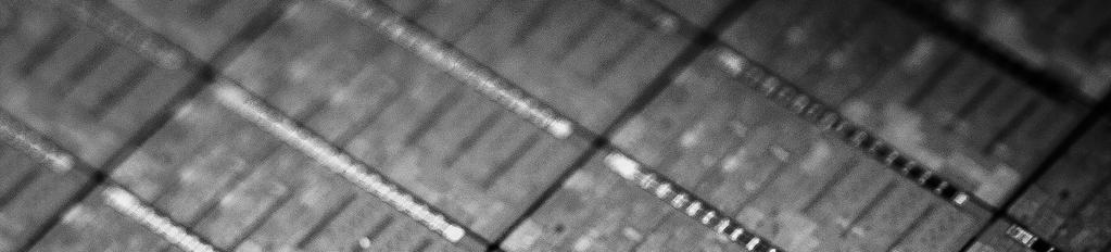
18 74 Advanced Metallization

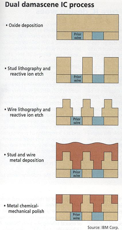
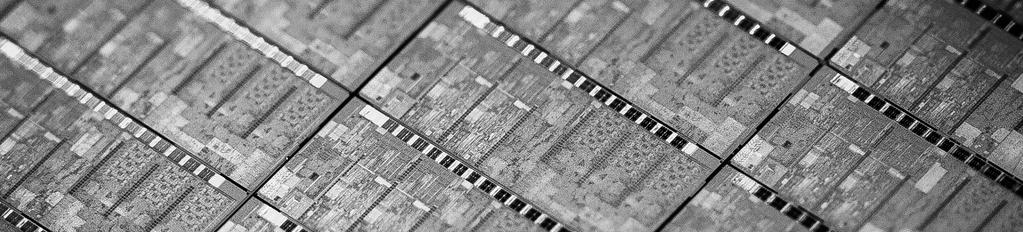
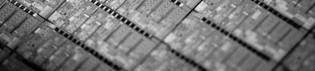
19 75 Advanced Metallization
20 CMOS Manufacturing process Circuit design Set of optical masks Fabrication process Circuit designer Design rule set Process engineer All material: Chap. 2 of J. Rabaey, A. Chandrakasan, B. Nikolic, Digital Integrated Circuits, second edition, Prentice Halls, 2002
21 Design Rules Minimum line width depend on lithographyand process Micron rules: absolute dimensions for intra-layer and inter-layer layouts 77


22 78 Layers in 0.25 µm CMOS process
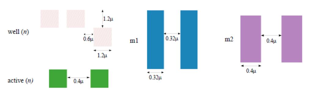
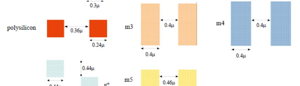
23 79 Intra-Layer Design Rules


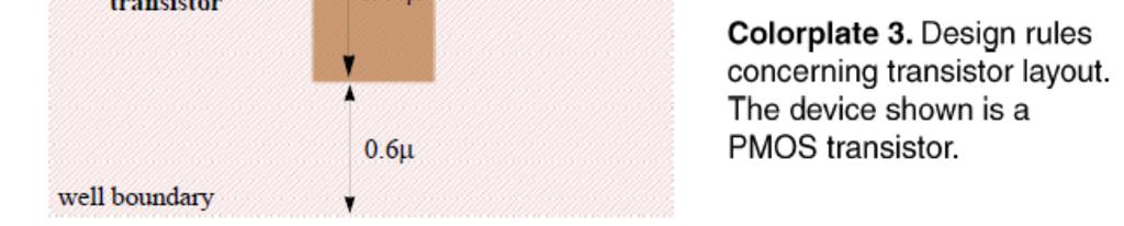
24 80 Transistor Layout

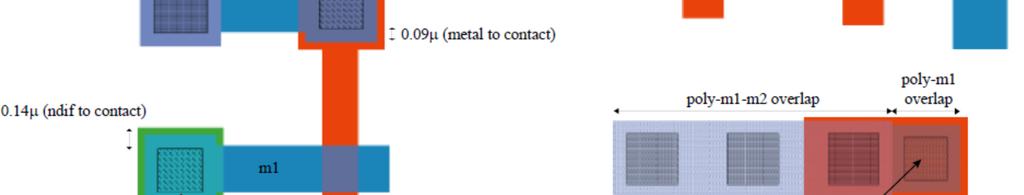
25 81 Vias and Contacts


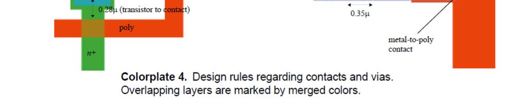
26 82 Select Layer

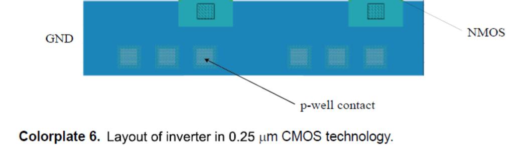
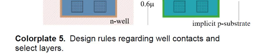
27 CMOS Inverter Layout

28 84 Layout Editor

29 Design Rule Checker poly_not_fet to all_diff minimum spacing = 0.14 um. 85
30 Sticks Diagram V DD 3 In 1 Out Dimensionless layout entities Only topology is important Final layout generated by compaction program GND Stick diagram of inverter 86
31 Packaging Requirements Electrical: Low parasitics Mechanical: Reliable and robust Thermal: Efficient heat removal Economical: Cheap 87
32 Bonding Techniques Wire Bonding Substrate Die Pad Lead Frame 88 Gold wires, large inductance
33 Tape-Automated Bonding (TAB) Sprocket hole Film + Pattern Solder Bump Test pads Die Lead frame Substrate (b) Die attachment using solder bumps. (a) Polymer Tape with imprinted wiring pattern. Polymer film 89
34 Flip-Chip Bonding Die Solder bumps Top (where circuit is) Interconnect layers Substrate 90
35 Package-to-Board Interconnect (a) Through-Hole Mounting (b) Surface Mount 91


36 Package Types DIP PLCC PGA 92
37 93 Package Parameters

38 94 Multi-Chip Modules
Manufacturing Process
 Digital Integrated Circuits A Design Perspective Jan M. Rabaey Anantha Chandrakasan Borivoje Nikolic Manufacturing Process July 30, 2002 1 CMOS Process 2 A Modern CMOS Process gate-oxide TiSi 2 AlCu Tungsten
ECE 659. Jan M. Rabaey Anantha Chandrakasan Borivoje Nikolic. July 30, Digital EE141 Integrated Circuits 2nd Manufacturing.
 Digital Integrated Circuits A Design Perspective Jan M. Rabaey Anantha Chandrakasan Borivoje Nikolic Manufacturing Process July 0, 00 1 CMOS Process 1 A Modern CMOS Process gate-oxide TiSi AlCu Tungsten
CMOS Manufacturing process. Circuit designer. Design rule set. Process engineer. Set of optical masks. Fabrication process.
 CMOS Manufacturing process Circuit design Set of optical masks Fabrication process Circuit designer Design rule set Process engineer All material: Chap. 2 of J. Rabaey, A. Chandrakasan, B. Nikolic, Digital
Manufacturing Process
 CMOS Manufacturing Process CMOS Process 1 A Modern CMOS Process gate-oxide TiSi AlCu Tungsten SiO n+ p-well p-epi poly n-well p+ SiO p+ Dual-Well Trench-Isolated CMOS Process Circuit Under Design V DD
CMOS Manufacturing Process
 CMOS Manufacturing Process CMOS Process A Modern CMOS Process gate-oxide TiSi 2 AlCu Tungsten SiO 2 n+ p-well p-epi poly n-well p+ SiO 2 p+ Dual-Well Trench-Isolated CMOS Process Circuit Under Design V
Chapter 2 Manufacturing Process
 Digital Integrated Circuits A Design Perspective Chapter 2 Manufacturing Process 1 CMOS Process 2 CMOS Process (n-well) Both NMOS and PMOS must be built in the same silicon material. PMOS in n-well NMOS
9/4/2008 GMU, ECE 680 Physical VLSI Design
 ECE680: Physical VLSI Design Chapter II CMOS Manufacturing Process 1 Dual-Well Trench-Isolated CMOS Process gate-oxide TiSi 2 AlCu Tungsten SiO 2 p-well poly n-well SiO 2 n+ p-epi p+ p+ 2 Schematic Layout
We are moving to 155 Donner Lab From Thursday, Feb 2 We will be able to accommodate everyone!
 -Spring 006 Digital Integrated Circuits Lecture 4 CMOS Manufacturing Process Design Rules EECS141 1 Good News! We are moving to 155 Donner Lab From Thursday, Feb We will be able to accommodate everyone!
Manufacturing Process
 Manufacturing Process 1 CMOS Process 2 A Modern CMOS Process gate-oxide TiSi 2 AlCu Tungsten SiO 2 n+ p-well p-epi poly n-well p+ SiO 2 p+ Dual-Well Trench-Isolated CMOS Process 3 Single-crystal ingot
Cost of Integrated Circuits
 Cost of IC Design 1 Cost of Integrated Circuits NRE (Non-Recurrent Engineering) costs fixed design time and effort, mask generation independent of sales volume / number of products one-time cost factor
Lecture 1A: Manufacturing& Layout
 Introduction to CMOS VLSI Design Lecture 1A: Manufacturing& Layout David Harris Harvey Mudd College Spring 2004 Steven Levitan Fall 2008 1 The Manufacturing Process For a great tour through the IC manufacturing
VLSI Design and Simulation
 VLSI Design and Simulation CMOS Processing Technology Topics CMOS Processing Technology Semiconductor Processing How do we make a transistor? Fabrication Process Wafer Processing Silicon single crystal
ECE321 Electronics I
 ECE321 Electronics I Lecture 19: CMOS Fabrication Payman Zarkesh-Ha Office: ECE Bldg. 230B Office hours: Tuesday 2:00-3:00PM or by appointment E-mail: payman@ece.unm.edu Slide: 1 Miller Effect Interconnect
VLSI PROCESS TECHNOLOGY By ER. HIMANSHU SHARMA
 VLSI PROCESS TECHNOLOGY y ER. HIMNSHU SHRM Fabrication Masks Chips Wafers Processing Processed Wafer Traditional CMOS Process Modern CMOS Process Dual-Well Trench-Isolated CMOS gate oxide field oxide l
CS/ECE 5710/6710. N-type Transistor. N-type from the top. Diffusion Mask. Polysilicon Mask. CMOS Processing
 CS/ECE 5710/6710 CMOS Processing Addison-Wesley N-type Transistor D G +Vgs + Vds S N-type from the top i electrons - Diffusion Mask Mask for just the diffused regions Top view shows patterns that make
PROCESS FLOW AN INSIGHT INTO CMOS FABRICATION PROCESS
 Contents: VI Sem ECE 06EC63: Analog and Mixed Mode VLSI Design PROCESS FLOW AN INSIGHT INTO CMOS FABRICATION PROCESS 1. Introduction 2. CMOS Fabrication 3. Simplified View of Fabrication Process 3.1 Alternative
FABRICATION of MOSFETs
 FABRICATION of MOSFETs CMOS fabrication sequence -p-type silicon substrate wafer -creation of n-well regions for pmos transistors, -impurity implantation into the substrate. -thick oxide is grown in the
UT Austin, ECE Department VLSI Design 2. CMOS Fabrication, Layout Rules
 2. CMOS Fabrication, Layout, Design Rules Last module: Introduction to the course How a transistor works CMOS transistors This module: CMOS Fabrication Design Rules CMOS Fabrication CMOS transistors are
Czochralski Crystal Growth
 Czochralski Crystal Growth Crystal Pulling Crystal Ingots Shaping and Polishing 300 mm wafer 1 2 Advantage of larger diameter wafers Wafer area larger Chip area larger 3 4 Large-Diameter Wafer Handling
Fabrication and Layout
 ECEN454 Digital Integrated Circuit Design Fabrication and Layout ECEN 454 3.1 A Glimpse at MOS Device Polysilicon Aluminum ECEN 475 4.2 1 Material Classification Insulators Glass, diamond, silicon oxide
CMOS Technology. Flow varies with process types & company. Start with substrate selection. N-Well CMOS Twin-Well CMOS STI
 CMOS Technology Flow varies with process types & company N-Well CMOS Twin-Well CMOS STI Start with substrate selection Type: n or p Doping level, resistivity Orientation, 100, or 101, etc Other parameters
EE 330 Lecture 9. IC Fabrication Technology Part II. -Oxidation -Epitaxy -Polysilicon -Planarization -Resistance and Capacitance in Interconnects
 EE 330 Lecture 9 IC Fabrication Technology Part II -Oxidation -Epitaxy -Polysilicon -Planarization -Resistance and Capacitance in Interconnects Review from Last Time Etching Dry etch (anisotropic) SiO
EE 330 Lecture 9. IC Fabrication Technology Part 2
 EE 330 Lecture 9 IC Fabrication Technology Part 2 Quiz 8 A 2m silicon crystal is cut into wafers using a wire saw. If the wire diameter is 220um and the wafer thickness is 350um, how many wafers will this
Chapter 3 CMOS processing technology
 Chapter 3 CMOS processing technology (How to make a CMOS?) Si + impurity acceptors(p-type) donors (n-type) p-type + n-type => pn junction (I-V) 3.1.1 (Wafer) Wafer = A disk of silicon (0.25 mm - 1 mm thick),
Silicon Wafer Processing PAKAGING AND TEST
 Silicon Wafer Processing PAKAGING AND TEST Parametrical test using test structures regularly distributed in the wafer Wafer die test marking defective dies dies separation die fixing (not marked as defective)
EE40 Lec 22. IC Fabrication Technology. Prof. Nathan Cheung 11/19/2009
 Suggested Reading EE40 Lec 22 IC Fabrication Technology Prof. Nathan Cheung 11/19/2009 300mm Fab Tour http://www-03.ibm.com/technology/manufacturing/technology_tour_300mm_foundry.html Overview of IC Technology
Integrated Circuits & Systems
 Federal University of Santa Catarina Center for Technology Computer Science & Electronics Engineering Integrated Circuits & Systems INE 5442 Lecture 6 CMOS Fabrication Process & Design Rules guntzel@inf.ufsc.br
Introduction to CMOS VLSI Design. Layout, Fabrication, and Elementary Logic Design
 Introduction to CMOS VLSI Design Layout, Fabrication, and Elementary Logic Design CMOS Fabrication CMOS transistors are fabricated on silicon wafer Lithography process similar to printing press On each
CMOS FABRICATION. n WELL PROCESS
 CMOS FABRICATION n WELL PROCESS Step 1: Si Substrate Start with p- type substrate p substrate Step 2: Oxidation Exposing to high-purity oxygen and hydrogen at approx. 1000 o C in oxidation furnace SiO
Lecture 0: Introduction
 Lecture 0: Introduction Introduction Integrated circuits: many transistors on one chip. Very Large Scale Integration (VLSI): bucketloads! Complementary Metal Oxide Semiconductor Fast, cheap, low power
EE 330 Lecture 9. IC Fabrication Technology Part II. -Oxidation -Epitaxy -Polysilicon -Planarization -Resistance and Capacitance in Interconnects
 EE 330 Lecture 9 IC Fabrication Technology Part II -Oxidation -Epitaxy -Polysilicon -Planarization -Resistance and Capacitance in Interconnects Review from Last Time IC Fabrication Technology Crystal Preparation
ECE520 VLSI Design. Lecture 7: CMOS Manufacturing Process. Payman Zarkesh-Ha
 ECE520 VLSI Design Lecture 7: CMOS Manufacturing Process Payman Zarkesh-Ha Office: ECE Bldg. 230B Office hours: Wednesday 2:00-3:00PM or by appointment E-mail: pzarkesh@unm.edu Slide: 1 Review of Last
EE 330 Lecture 8. IC Fabrication Technology Part II. - Oxidation - Epitaxy - Polysilicon - Interconnects
 EE 330 Lecture 8 IC Fabrication Technology Part II - Oxidation - Epitaxy - Polysilicon - Interconnects Review from Last Time MOS Transistor Bulk Source Gate Drain p-channel MOSFET Lightly-doped n-type
CMOS VLSI Design. Introduction. All materials are from the textbook Weste and Harris, 3 rd Edition CMOS VLSI DESIGN. Introduction
 CMOS VLSI Design Introduction ll materials are from the textbook Weste and Harris, 3 rd Edition CMOS VLSI DESIGN Introduction Chapter previews the entire field, subsequent chapters elaborate on specific
Department of Electrical Engineering. Jungli, Taiwan
 Chapter 3 Fabrication of CMOS Integrated Circuits Jin-Fu Li Department of Electrical Engineering National Central University Jungli, Taiwan Background Outline The CMOS Process Flow Design Rules Latchup
VLSI INTRODUCTION P.VIDYA SAGAR ( ASSOCIATE PROFESSOR) Department of Electronics and Communication Engineering, VBIT
 Department of Electronics and Communication Engineering, VBIT") VLSI INTRODUCTION P.VIDYA SAGAR ( ASSOCIATE PROFESSOR) contents UNIT I INTRODUCTION: Introduction to IC Technology MOS, PMOS, NMOS, CMOS & BiCMOS technologies. BASIC ELECTRICAL PROPERTIES : Basic Electrical
VLSI INTRODUCTION P.VIDYA SAGAR ( ASSOCIATE PROFESSOR) contents UNIT I INTRODUCTION: Introduction to IC Technology MOS, PMOS, NMOS, CMOS & BiCMOS technologies. BASIC ELECTRICAL PROPERTIES : Basic Electrical
VLSI. Lecture 1. Jaeyong Chung System-on-Chips (SoC) Laboratory Incheon National University. Based on slides of David Money Harris
 Laboratory Incheon National University. Based on slides of David Money Harris") VLSI Lecture 1 Jaeyong Chung System-on-Chips (SoC) Laboratory Incheon National University Based on slides of David Money Harris Goals of This Course Learn the principles of VLSI design Learn to design
VLSI Lecture 1 Jaeyong Chung System-on-Chips (SoC) Laboratory Incheon National University Based on slides of David Money Harris Goals of This Course Learn the principles of VLSI design Learn to design
Chapter 3 Silicon Device Fabrication Technology
 Chapter 3 Silicon Device Fabrication Technology Over 10 15 transistors (or 100,000 for every person in the world) are manufactured every year. VLSI (Very Large Scale Integration) ULSI (Ultra Large Scale
CMOS Fabrication. Dr. Bassam Jamil. Adopted from slides of the textbook
 CMOS Fabrication Dr. Bassam Jamil Adopted from slides of the textbook CMOS Fabrication CMOS transistors are fabricated on silicon wafer Lithography process similar to printing press On each step, different
THE MANUFACTURING PROCESS
 chapter2.fm Page 33 Monday, September 4, 2000 11:11 AM CHAPTER 2 THE MANUFACTURING PROCESS Overview of manufacturing process n Design rules n IC packaging n Future Trends in Integrated Circuit Technology
Mostafa Soliman, Ph.D. May 5 th 2014
 Mostafa Soliman, Ph.D. May 5 th 2014 Mostafa Soliman, Ph.D. 1 Basic MEMS Processes Front-End Processes Back-End Processes 2 Mostafa Soliman, Ph.D. Wafers Deposition Lithography Etch Chips 1- Si Substrate
CHAPTER - 4 CMOS PROCESSING TECHNOLOGY
 CHAPTER - 4 CMOS PROCESSING TECHNOLOGY Samir kamal Spring 2018 4.1 CHAPTER OBJECTIVES 1. Introduce the CMOS designer to the technology that is responsible for the semiconductor devices that might be designed
INTEGRATED-CIRCUIT TECHNOLOGY
 INTEGRATED-CIRCUIT TECHNOLOGY 0. Silicon crystal growth and wafer preparation 1. Processing Steps 1.1. Photolitography 1.2. Oxidation 1.3. Layer Deposition 1.4. Etching 1.5. Diffusion 1.6 Backend: assembly,
Microelectronics. Integrated circuits. Introduction to the IC technology M.Rencz 11 September, Expected decrease in line width
 Microelectronics Introduction to the IC technology M.Rencz 11 September, 2002 9/16/02 1/37 Integrated circuits Development is controlled by the roadmaps. Self-fulfilling predictions for the tendencies
conductor - gate insulator source gate n substrate conductor - gate insulator gate substrate n open switch closed switch however: closed however:
 MOS Transistors Readings: Chapter 1 N-type drain conductor - gate insulator source gate drain source n p n substrate P-type drain conductor - gate insulator source drain gate source p p substrate n 42
FABRICATION OF CMOS INTEGRATED CIRCUITS. Dr. Mohammed M. Farag
 FABRICATION OF CMOS INTEGRATED CIRCUITS Dr. Mohammed M. Farag Outline Overview of CMOS Fabrication Processes The CMOS Fabrication Process Flow Design Rules EE 432 VLSI Modeling and Design 2 CMOS Fabrication
Lect. 2: Basics of Si Technology
 Unit processes Thin Film Deposition Etching Ion Implantation Photolithography Chemical Mechanical Polishing 1. Thin Film Deposition Layer of materials ranging from fractions of nanometer to several micro-meters
Isolation Technology. Dr. Lynn Fuller
 ROCHESTER INSTITUTE OF TECHNOLOGY MICROELECTRONIC ENGINEERING Isolation Technology Dr. Lynn Fuller Motorola Professor 82 Lomb Memorial Drive Rochester, NY 14623-5604 Tel (585) 475-2035 Fax (585) 475-5041
Semiconductor Manufacturing Technology. IC Fabrication Process Overview
 Semiconductor Manufacturing Technology Michael Quirk & Julian Serda October 00 by Prentice Hall Chapter 9 IC Fabrication Process Overview /4 Objectives After studying the material in this chapter, you
EE 560 FABRICATION OF MOS CIRCUITS. Kenneth R. Laker, University of Pennsylvania
 1 EE 560 FABRICATION OF MOS CIRCUITS 2 CMOS CHIP MANUFACTRING STEPS Substrate Wafer Wafer Fabrication (diffusion, oxidation, photomasking, ion implantation, thin film deposition, etc.) Finished Wafer Wafer
Lecture #18 Fabrication OUTLINE
 Transistors on a Chip Lecture #18 Fabrication OUTLINE IC Fabrication Technology Introduction the task at hand Doping Oxidation Thin-film deposition Lithography Etch Lithography trends Plasma processing
EEC 118 Lecture #5: MOS Fabrication. Rajeevan Amirtharajah University of California, Davis Jeff Parkhurst Intel Corporation
 EEC 118 Lecture #5: MOS Fabrication Rajeevan Amirtharajah University of California, Davis Jeff Parkhurst Intel Corporation Announcements Lab 3 this week, report due next week HW 3 due this Friday at 4
Chapter 4 : ULSI Process Integration (0.18 m CMOS Process)
") Chapter : ULSI Process Integration (0.8 m CMOS Process) Reference. Semiconductor Manufacturing Technology : Michael Quirk and Julian Serda (00). - (00). Semiconductor Physics and Devices- Basic Principles(/e)
Chapter : ULSI Process Integration (0.8 m CMOS Process) Reference. Semiconductor Manufacturing Technology : Michael Quirk and Julian Serda (00). - (00). Semiconductor Physics and Devices- Basic Principles(/e)
EE 434 Lecture 9. IC Fabrication Technology
 EE 434 Lecture 9 IC Fabrication Technology Quiz 7 The layout of a film resistor with electrodes A and B is shown. If the sheet resistance of the film is 40 /, determine the resistance between nodes A and
Lecture 19 Microfabrication 4/1/03 Prof. Andy Neureuther
 EECS 40 Spring 2003 Lecture 19 Microfabrication 4/1/03 Prof. ndy Neureuther How are Integrated Circuits made? Silicon wafers Oxide formation by growth or deposition Other films Pattern transfer by lithography
Microfabrication of Integrated Circuits
 Microfabrication of Integrated Circuits OUTLINE History Basic Processes Implant; Oxidation; Photolithography; Masks Layout and Process Flow Device Cross Section Evolution Lecture 38, 12/05/05 Reading This
EE 143 FINAL EXAM NAME C. Nguyen May 10, Signature:
 INSTRUCTIONS Read all of the instructions and all of the questions before beginning the exam. There are 5 problems on this Final Exam, totaling 143 points. The tentative credit for each part is given to
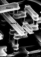
Complexity of IC Metallization. Early 21 st Century IC Technology
 EECS 42 Introduction to Digital Electronics Lecture # 25 Microfabrication Handout of This Lecture. Today: how are Integrated Circuits made? Silicon wafers Oxide formation by growth or deposition Other
Review of CMOS Processing Technology
 - Scaling and Integration Moore s Law Unit processes Thin Film Deposition Etching Ion Implantation Photolithography Chemical Mechanical Polishing 1. Thin Film Deposition Layer of materials ranging from
Figure 2.3 (cont., p. 60) (e) Block diagram of Pentium 4 processor with 42 million transistors (2000). [Courtesy Intel Corporation.
 (e) Block diagram of Pentium 4 processor with 42 million transistors (2000). [Courtesy Intel Corporation.") Figure 2.1 (p. 58) Basic fabrication steps in the silicon planar process: (a) oxide formation, (b) selective oxide removal, (c) deposition of dopant atoms on wafer, (d) diffusion of dopant atoms into exposed
Figure 2.1 (p. 58) Basic fabrication steps in the silicon planar process: (a) oxide formation, (b) selective oxide removal, (c) deposition of dopant atoms on wafer, (d) diffusion of dopant atoms into exposed
Fabrication and Layout
 Fabrication and Layout Kenneth Yun UC San Diego Adapted from EE271 notes, Stanford University Overview Semiconductor properties How chips are made Design rules for layout Reading Fabrication: W&E 3.1,
VLSI Digital Systems Design
 VLSI Digital Systems Design CMOS Processing cmpe222_03process_ppt.ppt 1 Si Purification Chemical purification of Si Zone refined Induction furnace Si ingot melted in localized zone Molten zone moved from
Lecture 2: CMOS Fabrication Mark McDermott Electrical and Computer Engineering The University of Texas at Austin
 Lecture 2: CMOS Fabrication Mark McDermott Electrical and Computer Engineering The University of Texas at Austin Agenda Last module: Introduction to the course How a transistor works CMOS transistors This
INTRODUCTION TO VLSI FABRICATION MATERIALS & PROCESSES. Primary Chip Ingredients
 INTRODUCTION TO VLSI FABRICATION MATERIALS & PROCESSES Primary Chi Ingredients 1) Silicon crystalline Near erfect crystal (atoms organized in a regular, ordered lattice) Semiconductor not a conductor or
Fabrication Process. Crystal Growth Doping Deposition Patterning Lithography Oxidation Ion Implementation CONCORDIA VLSI DESIGN LAB
 Fabrication Process Crystal Growth Doping Deposition Patterning Lithography Oxidation Ion Implementation 1 Fabrication- CMOS Process Starting Material Preparation 1. Produce Metallurgical Grade Silicon
Lecture 030 Integrated Circuit Technology - I (5/8/03) Page 030-1
 Page 030-1") Lecture 030 Integrated Circuit Technology - I (5/8/03) Page 030-1 LECTURE 030 INTEGRATED CIRCUIT TECHNOLOGY - I (References [7,8]) Objective The objective of this presentation is: 1.) Illustrate integrated
Lecture 030 Integrated Circuit Technology - I (5/8/03) Page 030-1 LECTURE 030 INTEGRATED CIRCUIT TECHNOLOGY - I (References [7,8]) Objective The objective of this presentation is: 1.) Illustrate integrated
ELEC 3908, Physical Electronics, Lecture 4. Basic Integrated Circuit Processing
 ELEC 3908, Physical Electronics, Lecture 4 Basic Integrated Circuit Processing Lecture Outline Details of the physical structure of devices will be very important in developing models for electrical behavior
KGC SCIENTIFIC Making of a Chip
 KGC SCIENTIFIC www.kgcscientific.com Making of a Chip FROM THE SAND TO THE PACKAGE, A DIAGRAM TO UNDERSTAND HOW CPU IS MADE? Sand CPU CHAIN ANALYSIS OF SEMICONDUCTOR Material for manufacturing process
IC/MEMS Fabrication - Outline. Fabrication
 IC/MEMS Fabrication - Outline Fabrication overview Materials Wafer fabrication The Cycle: Deposition Lithography Etching Fabrication IC Fabrication Deposition Spin Casting PVD physical vapor deposition
Microelettronica. Planar Technology for Silicon Integrated Circuits Fabrication. 26/02/2017 A. Neviani - Microelettronica
 Microelettronica Planar Technology for Silicon Integrated Circuits Fabrication 26/02/2017 A. Neviani - Microelettronica Introduction Simplified crosssection of an nmosfet and a pmosfet Simplified crosssection
EE 330 Lecture 8. IC Fabrication Technology Part II. - Masking - Photolithography - Deposition - Etching - Diffusion
 EE 330 Lecture 8 IC Fabrication Technology Part II?? - Masking - Photolithography - Deposition - Etching - Diffusion Review from Last Time Technology Files Provide Information About Process Process Flow
Low Power VLSI Circuits and Systems Prof. Ajit Pal Department of Computer Science and Engineering Indian Institute of Technology, Kharagpur
 Low Power VLSI Circuits and Systems Prof. Ajit Pal Department of Computer Science and Engineering Indian Institute of Technology, Kharagpur Lecture No. # 02 MOS Transistors - I Hello and welcome to today
Lecture 22: Integrated circuit fabrication
 Lecture 22: Integrated circuit fabrication Contents 1 Introduction 1 2 Layering 4 3 Patterning 7 4 Doping 8 4.1 Thermal diffusion......................... 10 4.2 Ion implantation.........................
CHAPTER 1 HOW SEMICONDUCTOR CHIPS ARE MADE
 CHAPTER 1 HOW SEMICONDUCTOR CHIPS ARE MADE Hwaiyu Geng Hewlett-Packard Company Palo Alto, California Lin Zhou Intel Corporation Hillsboro, Oregon 1.1 INTRODUCTION Over the past decades, an information
The Physical Structure (NMOS)
") The Physical Structure (NMOS) Al SiO2 Field Oxide Gate oxide S n+ Polysilicon Gate Al SiO2 SiO2 D n+ L channel P Substrate Field Oxide contact Metal (S) n+ (G) L W n+ (D) Poly 1 3D Perspective 2 3 Fabrication
The Physical Structure (NMOS) Al SiO2 Field Oxide Gate oxide S n+ Polysilicon Gate Al SiO2 SiO2 D n+ L channel P Substrate Field Oxide contact Metal (S) n+ (G) L W n+ (D) Poly 1 3D Perspective 2 3 Fabrication
EE CMOS TECHNOLOGY- Chapter 2 in the Text
 1 EE 212 FALL 1999-00 CMOS TECHOLOGY- Chapter 2 in the Text In this set of notes we will describe a modern CMOS process flow. In the simplest CMOS technologies, we need to realize simply MOS and MOS transistors
Microstructure of Electronic Materials. Amorphous materials. Single-Crystal Material. Professor N Cheung, U.C. Berkeley
 Microstructure of Electronic Materials Amorphous materials Single-Crystal Material 1 The Si Atom The Si Crystal diamond structure High-performance semiconductor devices require defect-free crystals 2 Crystallographic
EECS130 Integrated Circuit Devices
 EECS130 Integrated Circuit Devices Professor Ali Javey 9/13/2007 Fabrication Technology Lecture 1 Silicon Device Fabrication Technology Over 10 15 transistors (or 100,000 for every person in the world)
Chapter 4 Fabrication Process of Silicon Carrier and. Gold-Gold Thermocompression Bonding
 Chapter 4 Fabrication Process of Silicon Carrier and Gold-Gold Thermocompression Bonding 4.1 Introduction As mentioned in chapter 2, the MEMs carrier is designed to integrate the micro-machined inductor
VLSI Systems and Computer Architecture Lab
 ΚΥΚΛΩΜΑΤΑ VLSI Πανεπιστήμιο Ιωαννίνων CMOS Technology Τμήμα Μηχανικών Η/Υ και Πληροφορικής 1 From the book: An Introduction ti to VLSI Process By: W. Maly ΚΥΚΛΩΜΑΤΑ VLSI Διάρθρωση 1. N well CMOS 2. Active
IC Fabrication Technology Part III Devices in Semiconductor Processes
 EE 330 Lecture 10 IC Fabrication Technology Part III Metalization and Interconnects Parasitic Capacitances Back-end Processes Devices in Semiconductor Processes Resistors Diodes Review from Last Lecture
Chapter 2 Problems. The CMOS technology we need to realize is shown below, from Figure 1-34 in the text. S P + N P + N WELL P +
 Chapter 2 roblems 2.1 Sketch a process flow that would result in the structure shown in Figure 1-34 by drawing a series of drawings similar to those in this chapter. You only need to describe the flow
Packaging and Ball Bonding Gold wire makes contact from bonding pads on chip to package Gold wire is formed into ball to make contact Uses an
 Packaging and Ball Bonding Gold wire makes contact from bonding pads on chip to package Gold wire is formed into ball to make contact Uses an ultrasonic process & heat Process called "Ball Bonding" Wedge
6.777J/2.732J Design and Fabrication of Microelectromechanical Devices Spring Term Solution to Problem Set 2 (16 pts)
") 6.777J/2.732J Design and Fabrication of Microelectromechanical Devices Spring Term 2007 By Brian Taff (Adapted from work by Feras Eid) Solution to Problem Set 2 (16 pts) Issued: Lecture 4 Due: Lecture
6.777J/2.732J Design and Fabrication of Microelectromechanical Devices Spring Term 2007 By Brian Taff (Adapted from work by Feras Eid) Solution to Problem Set 2 (16 pts) Issued: Lecture 4 Due: Lecture
This Appendix discusses the main IC fabrication processes.
 IC Fabrication B B.1 Introduction This Appendix discusses the main IC fabrication processes. B.2 NMOS fabrication NMOS transistors are formed in a p-type substrate. The NMOS fabrication process requires
Intel Pentium Processor W/MMX
 Construction Analysis Intel Pentium Processor W/MMX Report Number: SCA 9706-540 Global Semiconductor Industry the Serving Since 1964 15022 N. 75th Street Scottsdale, AZ 85260-2476 Phone: 602-998-9780 Fax:
Process Integration. MEMS Release Techniques Sacrificial Layer Removal Substrate Undercut
 Process Integration Self-aligned Techniques LOCOS- self-aligned channel stop Self-aligned Source/Drain Lightly Doped Drain (LDD) Self-aligned silicide (SALICIDE) Self-aligned oxide gap MEMS Release Techniques
Motorola PC603R Microprocessor
 Construction Analysis Motorola PC603R Microprocessor Report Number: SCA 9709-551 Global Semiconductor Industry the Serving Since 1964 17350 N. Hartford Drive Scottsdale, AZ 85255 Phone: 602-515-9780 Fax:
Fabrication Technology
 Fabrication Technology By B.G.Balagangadhar Department of Electronics and Communication Ghousia College of Engineering, Ramanagaram 1 OUTLINE Introduction Why Silicon The purity of Silicon Czochralski
EE 5344 Introduction to MEMS. CHAPTER 3 Conventional Si Processing
 3. Conventional licon Processing Micromachining, Microfabrication. EE 5344 Introduction to MEMS CHAPTER 3 Conventional Processing Why silicon? Abundant, cheap, easy to process. licon planar Integrated
Schematic creation of MOS field effect transistor.
 Schematic creation of MOS field effect transistor. Gate electrode Drain electrode Source electrode Gate oxide Gate length Page 1 Step 0 The positively doped silicon wafer is first coated with an insulating
EE6303 LINEAR INTEGRATED CIRCUITS AND APPLICATIONS 2 MARK QUESTIONS WITH ANSWERS UNIT I IC FABRICATION
 SRI VENKATESWARA COLLEGE OF ENGINEERING AND TECHNOLOGY TIRUPACHUR DEPARTMENT OFELECTRICAL AND ELECTRONICS ENGINEERING EE6303 LINEAR INTEGRATED CIRCUITS AND APPLICATIONS 1. Define an Integrated circuit.
Process Integration. NMOS Generic NMOS Process Flow. CMOS - The MOSIS Process Flow
 Process Integration Self-aligned Techniques LOCOS- self-aligned channel stop Self-aligned Source/Drain Lightly Doped Drain (LDD) Self-aligned silicide (SALICIDE) Self-aligned oxide gap MEMS Release Techniques
CSCI 4974 / 6974 Hardware Reverse Engineering. Lecture 5: Fabrication processes
 CSCI 4974 / 6974 Hardware Reverse Engineering Lecture 5: Fabrication processes QUIZ 3: CMOS layout Quiz Discussion Rationale If you know how something is put together, you can figure out how to take it
CMOS Processing Technology
 CHAPTER 2 CMOS Processing Technology Outline 2 1. CMOS Technologies 2. Layout Design Rules 3. CMOS Process Enhancements 4. Technology-related CAD Issues 5. Manufacturing Issues CMOS Technologies 3 n-well
Making of a Chip Illustrations
 Making of a Chip Illustrations 22nm 3D/Trigate Transistors Version April 2015 1 The illustrations on the following foils are low resolution images that visually support the explanations of the individual
CMOS Processing Technology
 CHAPTER 2 CMOS Processing Technology Outline 2 1. CMOS Technologies 2. Layout Design Rules 3. CMOS Process Enhancements 4. Technology-related CAD Issues 5. Manufacturing Issues CMOS Technologies 3 n-well