Chapter 2 Manufacturing Process
|
|
|
- Geraldine Newman
- 5 years ago
- Views:
Transcription

1 Digital Integrated Circuits A Design Perspective Chapter 2 Manufacturing Process 1
2 CMOS Process 2

3 CMOS Process (n-well) Both NMOS and PMOS must be built in the same silicon material. PMOS in n-well NMOS in p-substrate 3
4 A Modern CMOS Process PMOS in n-well NMOS in p-well gate-oxide TiSi 2 AlCu Tungsten SiO 2 n+ p-well p-epi poly n-well p+ SiO 2 p+ Dual-Well Trench-Isolated CMOS Process 4
5 Circuit Under Design V DD V DD M2 M4 V in V out V out2 M1 M3 5

6 Its Layout View 6
7 The Manufacturing Process For a great tour through the IC manufacturing process and its different steps, check 7

8 Silicon Wafer A single crystal ingot cut into thin slices. Diameters: 4-12 inches 8


.")
9 Photo-Lithographic Process oxidation optical mask photoresist removal (ashing) photoresist coating stepper exposure process step Typical operations in a single photolithographic cycle (from [Fullman]). spin, rinse, dry acid etch photoresist development 9
10 Photo-Lithographic Process (2) Oxidation layering this optional step deposits a thin layer of SiO2 over the complete wafer by exposing it to a mixture of high-purity oxygen and hydrogen at approximately 1000 C. The oxide is used as an insulation layer and also forms transistor gates. Photoresist coating a light sensitive polymer is evenly applied to a thickness of approximately 1µm by spinning the wafer. Positive photoresist Negative photoresist Stepper exposure a glass mask containing the patterns that we want to transfer to the silicon is brought in close proximity to the wafer. Photoresist development and bake the wafer are developed in either an acid or base solution to remove the nonexposed areas of photoresist. Once the exposed photoresist is removed, the wafer is soft baked at a low temperature to harden the remaining photoresist. 10
11 Photo-Lithographic Process (3) Acid etching material is selectively removed from areas of the wafer that are not covered by photoresist. Spin, rinse, and dry a special tool (called SRD) cleans the wafer with deionized water and dries it with nitrogen. Various process steps ion implantation, plasma etching, metal deposition, and so on. Photoresist removal (or ashing) a high-temperature plasma is used to selectively remove the remaining photoresist without damaging device layers. 11
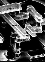
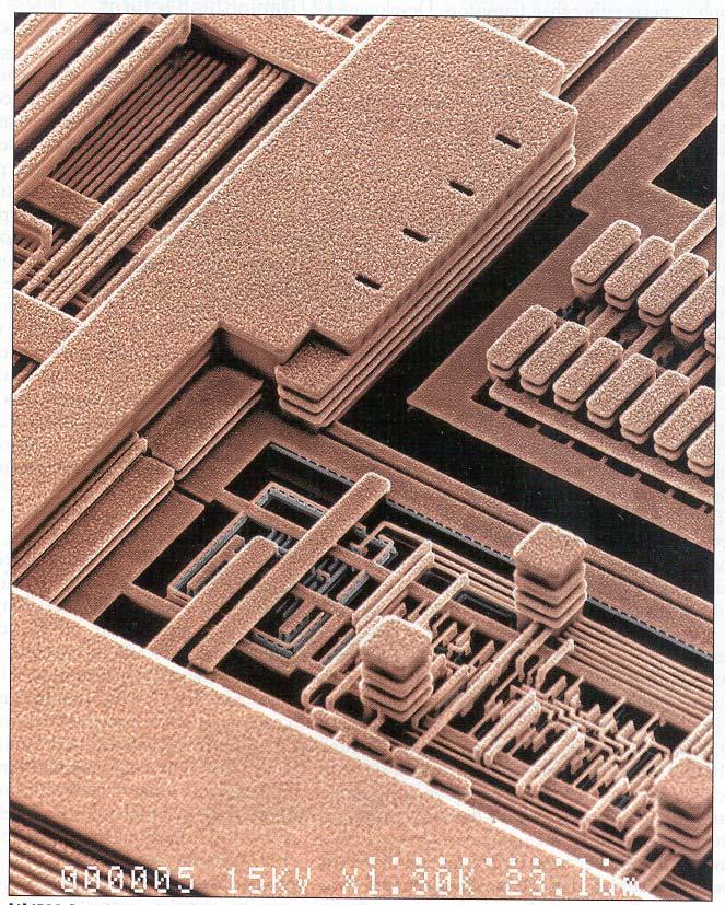
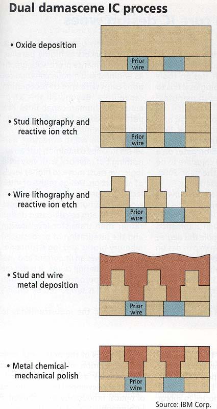
12 Patterning of SiO2 Si-substrate (a) Silicon base material Si-substrate Photoresist SiO 2 Si-substrate Chemical or plasma etch Hardened resist SiO 2 (d) After development and etching of resist, chemical or plasma etch of SiO 2 (b) After oxidation and deposition of negative photoresist Hardened resist SiO 2 UV-light Patterned optical mask Si-substrate (e) After etching Exposed resist SiO 2 Si-substrate (c) Stepper exposure Si-substrate (f) Final result after removal of resist 12
13 Recurring Process Steps (1) Diffusion and Ion Implantation Diffusion implantation: The wafers are placed in a quartz tube embedded in a heated furnace. A gas containing the dopant is introduced in the tube. The dopants diffuse into the exposed surface both vertically and horizontally. Ion implantation: Dopants are introduced as ions into the material. The ion implantation system directs and sweeps a beam of purified ions over the semiconductor surface. Advantage: It allows for an independent control of depth and dosage. Disadvantage: it damages the lattice of the semiconductor. The annealing step, in which the wafer is heated to around 1000 C for 15 to 30 minutes, and then allowed to cool slowly, is needed. 13
14 Recurring Process Steps (2) Deposition CMOS process requires the repetitive deposition of layers of a material over the complete wafer, to either act as buffers for a processing step, or as insulating or conducting layers. Etching: Once a material has been deposited, etching is used selectively to form patterns such as wires, contact hole, and etc. Wet etching method etches material both vertically and horizontally, and dry etching method etches material only vertically. Planarization: To reliably deposit a layer of material onto the semiconductor surface, it is essential that the surface be approximately flat. 14
15 CMOS Process Flow Define active areas Etch and fill trenches Implant well regions Deposit and pattern polysilicon layer Implant source and drain regions and substrate contacts Create contact and via windows Deposit and pattern metal layers 15
16 CMOS Process Walk-Through (1) p-epi p+ (a) Base material: p+ substrate with p-epi layer p-epi p+ Si 3 N 4 SiO 2 (b) After deposition of gate-oxide and sacrificial nitride (acts as a buffer layer) p+ (c) After plasma etch of insulating trenches using the inverse of the active area mask 16
17 CMOS Process Walk-Through (2) SiO 2 (d) After trench filling, CMP planarization, and removal of sacrificial nitride n (e) After n-well and V Tp adjust implants p (f) After p-well and V Tn adjust implants 17
18 CMOS Process Walk-Through (3) poly(silicon) (g) After polysilicon deposition and etch n+ p+ (h) After n+ source/drain and p+ source/drain implants. These steps also dope the polysilicon. SiO 2 (i) After deposition of SiO 2 insulator and contact hole etch. 18
19 CMOS Process Walk-Through (4) Al (j) After deposition and patterning of first Al layer. Al SiO 2 (k) After deposition of SiO 2 insulator, etching of via s, deposition and patterning of second layer of Al. 19
20 Advanced Metallization 20
21 Advanced Metallization 21
22 Layout and Design Rules 22

23 3D Perspective Polysilicon Aluminum 23
24 Design Rules Interface between designer and process engineer Guidelines for constructing process masks Unit dimension: Minimum line width Design rules: Width, Space, Clearance, Extension, and Overlap 24
25 Design Rules Width and Space Width Space 25
26 Design Rules Clearance Unrelated Related 26
27 Design Rules Extension and Overlap Extension Overlap 27
28 CMOS Process Layers Layer Well (p,n) Active Area (n+,p+) Select (p+,n+) Polysilicon Metal1 Metal2 Contact To Poly Contact To Diffusion Via Color Yellow Green Green Red Blue Magenta Black Black Black Representation 28

29 Layers in 0.25 µm m CMOS process 29
30 Intra-Layer Design Rules Same Potential Different Potential Well 10 0 or 6 9 Polysilicon 2 2 Active Select Contact or Via Hole 2 2 Metal1 Metal
31 Transistor Layout Transistor
32 Vias and Contacts 2 1 Via Metal to Active Contact 1 Metal to Poly Contact
33 Select Layer Select Substrate Well 33
34 CMOS Inverter Layout GND In V DD A A Out (a) Layout A A p-substrate n Field Oxide n + (b) Cross-Section along A-A 34 p +

35 Layout Editor - max It is developed at the University of California at Berkeley. 35

36 Layout Editor - Virtuoso 36
37 Layout Editor - Laker 37
 Off-line DRC:")
38 Design Rule Checker DRC (Design Rule Check) Using CAD tools to verify the layout On-line DRC: Diva (Virtuoso) Off-line DRC: Dracula 38
39 Symbolic Layout Full-custom VS Cell-Based Symbolic Layout The designer only draw a shorthand notation for the layout structure (transistors, contacts, wires). Advantage: designers don t care design rules Disadvantages: The density is unpredictable. 39
40 Sticks Diagram V DD 3 In 1 Out Dimensionless layout entities Only topology is important Final layout generated by compaction program GND Stick diagram of inverter 40
41 Layout Example - Inverter 41

42 Design Example - NAND (1) 42


43 Design Example NAND (2) 43
44 Packaging 44
45 Packaging Requirements Requirements Electrical: Low parasitics Mechanical: Reliable and robust Thermal: Efficient heat removal Commercial: 0~75 C Military: -55~125 C Economical: Cheap Materials Plastics Up to 2 W Ceramic Al 2 O 3 (Alumina) Up to 20 W Disadvantage: High dielectric constant => Large interconnect capacitance 45
46 Wire Bonding Substrate Die Pad Lead Frame Wires materials: Aluminum or gold Disadvantages: Longer manufacturing Wire distance Hard to predict parasitics 46
47 Tape-Automated Bonding (TAB) Sprocket hole Film + Pattern Solder Bump Test pads Lead frame Polymer film Die Substrate (b) Die attachment using solder bumps. (a) Polymer Tape with imprinted wiring pattern. 47
48 Flip-Chip Bonding Die Solder bumps Interconnect layers Substrate 48
49 Package-to to-board Interconnect (a) Through-Hole Mounting (b) Surface Mount 49

50 Package Types 1. Bare die 2. DIP 3. PGA 4. Small-outline IC 5. Quad flat pack 6. PLCC 7. Leadless carrier 50
51 Package Parameters 51

52 Multi-Chip Modules 52
53 Trend in Process Now: LDD (Lightly Doped Drain) Silicide Short-Term Copper and Low-k Dilectric SOI (Silicon on Insulator) Long-Term 3-D integrated circuits 53
Manufacturing Process
 Digital Integrated Circuits A Design Perspective Jan M. Rabaey Anantha Chandrakasan Borivoje Nikolic Manufacturing Process July 30, 2002 1 CMOS Process 2 A Modern CMOS Process gate-oxide TiSi 2 AlCu Tungsten
ECE 659. Jan M. Rabaey Anantha Chandrakasan Borivoje Nikolic. July 30, Digital EE141 Integrated Circuits 2nd Manufacturing.
 Digital Integrated Circuits A Design Perspective Jan M. Rabaey Anantha Chandrakasan Borivoje Nikolic Manufacturing Process July 0, 00 1 CMOS Process 1 A Modern CMOS Process gate-oxide TiSi AlCu Tungsten
9/4/2008 GMU, ECE 680 Physical VLSI Design
 ECE680: Physical VLSI Design Chapter II CMOS Manufacturing Process 1 Dual-Well Trench-Isolated CMOS Process gate-oxide TiSi 2 AlCu Tungsten SiO 2 p-well poly n-well SiO 2 n+ p-epi p+ p+ 2 Schematic Layout
CMOS Manufacturing process. Design rule set
 CMOS Manufacturing process Circuit design Set of optical masks Fabrication process Circuit designer Design rule set Process engineer All material: Chap. 2 of J. Rabaey, A. Chandrakasan, B. Nikolic, Digital
Manufacturing Process
 CMOS Manufacturing Process CMOS Process 1 A Modern CMOS Process gate-oxide TiSi AlCu Tungsten SiO n+ p-well p-epi poly n-well p+ SiO p+ Dual-Well Trench-Isolated CMOS Process Circuit Under Design V DD
CMOS Manufacturing Process
 CMOS Manufacturing Process CMOS Process A Modern CMOS Process gate-oxide TiSi 2 AlCu Tungsten SiO 2 n+ p-well p-epi poly n-well p+ SiO 2 p+ Dual-Well Trench-Isolated CMOS Process Circuit Under Design V
We are moving to 155 Donner Lab From Thursday, Feb 2 We will be able to accommodate everyone!
 -Spring 006 Digital Integrated Circuits Lecture 4 CMOS Manufacturing Process Design Rules EECS141 1 Good News! We are moving to 155 Donner Lab From Thursday, Feb We will be able to accommodate everyone!
Manufacturing Process
 Manufacturing Process 1 CMOS Process 2 A Modern CMOS Process gate-oxide TiSi 2 AlCu Tungsten SiO 2 n+ p-well p-epi poly n-well p+ SiO 2 p+ Dual-Well Trench-Isolated CMOS Process 3 Single-crystal ingot
Cost of Integrated Circuits
 Cost of IC Design 1 Cost of Integrated Circuits NRE (Non-Recurrent Engineering) costs fixed design time and effort, mask generation independent of sales volume / number of products one-time cost factor
VLSI Design and Simulation
 VLSI Design and Simulation CMOS Processing Technology Topics CMOS Processing Technology Semiconductor Processing How do we make a transistor? Fabrication Process Wafer Processing Silicon single crystal
Lecture 1A: Manufacturing& Layout
 Introduction to CMOS VLSI Design Lecture 1A: Manufacturing& Layout David Harris Harvey Mudd College Spring 2004 Steven Levitan Fall 2008 1 The Manufacturing Process For a great tour through the IC manufacturing
CMOS Manufacturing process. Circuit designer. Design rule set. Process engineer. Set of optical masks. Fabrication process.
 CMOS Manufacturing process Circuit design Set of optical masks Fabrication process Circuit designer Design rule set Process engineer All material: Chap. 2 of J. Rabaey, A. Chandrakasan, B. Nikolic, Digital
Fabrication and Layout
 ECEN454 Digital Integrated Circuit Design Fabrication and Layout ECEN 454 3.1 A Glimpse at MOS Device Polysilicon Aluminum ECEN 475 4.2 1 Material Classification Insulators Glass, diamond, silicon oxide
CMOS FABRICATION. n WELL PROCESS
 CMOS FABRICATION n WELL PROCESS Step 1: Si Substrate Start with p- type substrate p substrate Step 2: Oxidation Exposing to high-purity oxygen and hydrogen at approx. 1000 o C in oxidation furnace SiO
CS/ECE 5710/6710. N-type Transistor. N-type from the top. Diffusion Mask. Polysilicon Mask. CMOS Processing
 CS/ECE 5710/6710 CMOS Processing Addison-Wesley N-type Transistor D G +Vgs + Vds S N-type from the top i electrons - Diffusion Mask Mask for just the diffused regions Top view shows patterns that make
Introduction to CMOS VLSI Design. Layout, Fabrication, and Elementary Logic Design
 Introduction to CMOS VLSI Design Layout, Fabrication, and Elementary Logic Design CMOS Fabrication CMOS transistors are fabricated on silicon wafer Lithography process similar to printing press On each
UT Austin, ECE Department VLSI Design 2. CMOS Fabrication, Layout Rules
 2. CMOS Fabrication, Layout, Design Rules Last module: Introduction to the course How a transistor works CMOS transistors This module: CMOS Fabrication Design Rules CMOS Fabrication CMOS transistors are
PROCESS FLOW AN INSIGHT INTO CMOS FABRICATION PROCESS
 Contents: VI Sem ECE 06EC63: Analog and Mixed Mode VLSI Design PROCESS FLOW AN INSIGHT INTO CMOS FABRICATION PROCESS 1. Introduction 2. CMOS Fabrication 3. Simplified View of Fabrication Process 3.1 Alternative
ECE321 Electronics I
 ECE321 Electronics I Lecture 19: CMOS Fabrication Payman Zarkesh-Ha Office: ECE Bldg. 230B Office hours: Tuesday 2:00-3:00PM or by appointment E-mail: payman@ece.unm.edu Slide: 1 Miller Effect Interconnect
Chapter 3 CMOS processing technology
 Chapter 3 CMOS processing technology (How to make a CMOS?) Si + impurity acceptors(p-type) donors (n-type) p-type + n-type => pn junction (I-V) 3.1.1 (Wafer) Wafer = A disk of silicon (0.25 mm - 1 mm thick),
VLSI PROCESS TECHNOLOGY By ER. HIMANSHU SHARMA
 VLSI PROCESS TECHNOLOGY y ER. HIMNSHU SHRM Fabrication Masks Chips Wafers Processing Processed Wafer Traditional CMOS Process Modern CMOS Process Dual-Well Trench-Isolated CMOS gate oxide field oxide l
Microelectronics. Integrated circuits. Introduction to the IC technology M.Rencz 11 September, Expected decrease in line width
 Microelectronics Introduction to the IC technology M.Rencz 11 September, 2002 9/16/02 1/37 Integrated circuits Development is controlled by the roadmaps. Self-fulfilling predictions for the tendencies
CHAPTER - 4 CMOS PROCESSING TECHNOLOGY
 CHAPTER - 4 CMOS PROCESSING TECHNOLOGY Samir kamal Spring 2018 4.1 CHAPTER OBJECTIVES 1. Introduce the CMOS designer to the technology that is responsible for the semiconductor devices that might be designed
THE MANUFACTURING PROCESS
 chapter2.fm Page 33 Monday, September 4, 2000 11:11 AM CHAPTER 2 THE MANUFACTURING PROCESS Overview of manufacturing process n Design rules n IC packaging n Future Trends in Integrated Circuit Technology
VLSI INTRODUCTION P.VIDYA SAGAR ( ASSOCIATE PROFESSOR) Department of Electronics and Communication Engineering, VBIT
 Department of Electronics and Communication Engineering, VBIT") VLSI INTRODUCTION P.VIDYA SAGAR ( ASSOCIATE PROFESSOR) contents UNIT I INTRODUCTION: Introduction to IC Technology MOS, PMOS, NMOS, CMOS & BiCMOS technologies. BASIC ELECTRICAL PROPERTIES : Basic Electrical
VLSI INTRODUCTION P.VIDYA SAGAR ( ASSOCIATE PROFESSOR) contents UNIT I INTRODUCTION: Introduction to IC Technology MOS, PMOS, NMOS, CMOS & BiCMOS technologies. BASIC ELECTRICAL PROPERTIES : Basic Electrical
FABRICATION of MOSFETs
 FABRICATION of MOSFETs CMOS fabrication sequence -p-type silicon substrate wafer -creation of n-well regions for pmos transistors, -impurity implantation into the substrate. -thick oxide is grown in the
Lecture 0: Introduction
 Lecture 0: Introduction Introduction Integrated circuits: many transistors on one chip. Very Large Scale Integration (VLSI): bucketloads! Complementary Metal Oxide Semiconductor Fast, cheap, low power
CMOS Fabrication. Dr. Bassam Jamil. Adopted from slides of the textbook
 CMOS Fabrication Dr. Bassam Jamil Adopted from slides of the textbook CMOS Fabrication CMOS transistors are fabricated on silicon wafer Lithography process similar to printing press On each step, different
Silicon Wafer Processing PAKAGING AND TEST
 Silicon Wafer Processing PAKAGING AND TEST Parametrical test using test structures regularly distributed in the wafer Wafer die test marking defective dies dies separation die fixing (not marked as defective)
CMOS Technology. Flow varies with process types & company. Start with substrate selection. N-Well CMOS Twin-Well CMOS STI
 CMOS Technology Flow varies with process types & company N-Well CMOS Twin-Well CMOS STI Start with substrate selection Type: n or p Doping level, resistivity Orientation, 100, or 101, etc Other parameters
ECE520 VLSI Design. Lecture 7: CMOS Manufacturing Process. Payman Zarkesh-Ha
 ECE520 VLSI Design Lecture 7: CMOS Manufacturing Process Payman Zarkesh-Ha Office: ECE Bldg. 230B Office hours: Wednesday 2:00-3:00PM or by appointment E-mail: pzarkesh@unm.edu Slide: 1 Review of Last
Department of Electrical Engineering. Jungli, Taiwan
 Chapter 3 Fabrication of CMOS Integrated Circuits Jin-Fu Li Department of Electrical Engineering National Central University Jungli, Taiwan Background Outline The CMOS Process Flow Design Rules Latchup
Czochralski Crystal Growth
 Czochralski Crystal Growth Crystal Pulling Crystal Ingots Shaping and Polishing 300 mm wafer 1 2 Advantage of larger diameter wafers Wafer area larger Chip area larger 3 4 Large-Diameter Wafer Handling
FABRICATION OF CMOS INTEGRATED CIRCUITS. Dr. Mohammed M. Farag
 FABRICATION OF CMOS INTEGRATED CIRCUITS Dr. Mohammed M. Farag Outline Overview of CMOS Fabrication Processes The CMOS Fabrication Process Flow Design Rules EE 432 VLSI Modeling and Design 2 CMOS Fabrication
Microfabrication of Integrated Circuits
 Microfabrication of Integrated Circuits OUTLINE History Basic Processes Implant; Oxidation; Photolithography; Masks Layout and Process Flow Device Cross Section Evolution Lecture 38, 12/05/05 Reading This
Lect. 2: Basics of Si Technology
 Unit processes Thin Film Deposition Etching Ion Implantation Photolithography Chemical Mechanical Polishing 1. Thin Film Deposition Layer of materials ranging from fractions of nanometer to several micro-meters
VLSI. Lecture 1. Jaeyong Chung System-on-Chips (SoC) Laboratory Incheon National University. Based on slides of David Money Harris
 Laboratory Incheon National University. Based on slides of David Money Harris") VLSI Lecture 1 Jaeyong Chung System-on-Chips (SoC) Laboratory Incheon National University Based on slides of David Money Harris Goals of This Course Learn the principles of VLSI design Learn to design
VLSI Lecture 1 Jaeyong Chung System-on-Chips (SoC) Laboratory Incheon National University Based on slides of David Money Harris Goals of This Course Learn the principles of VLSI design Learn to design
Complexity of IC Metallization. Early 21 st Century IC Technology
 EECS 42 Introduction to Digital Electronics Lecture # 25 Microfabrication Handout of This Lecture. Today: how are Integrated Circuits made? Silicon wafers Oxide formation by growth or deposition Other
Lecture 19 Microfabrication 4/1/03 Prof. Andy Neureuther
 EECS 40 Spring 2003 Lecture 19 Microfabrication 4/1/03 Prof. ndy Neureuther How are Integrated Circuits made? Silicon wafers Oxide formation by growth or deposition Other films Pattern transfer by lithography
EE40 Lec 22. IC Fabrication Technology. Prof. Nathan Cheung 11/19/2009
 Suggested Reading EE40 Lec 22 IC Fabrication Technology Prof. Nathan Cheung 11/19/2009 300mm Fab Tour http://www-03.ibm.com/technology/manufacturing/technology_tour_300mm_foundry.html Overview of IC Technology
CMOS VLSI Design. Introduction. All materials are from the textbook Weste and Harris, 3 rd Edition CMOS VLSI DESIGN. Introduction
 CMOS VLSI Design Introduction ll materials are from the textbook Weste and Harris, 3 rd Edition CMOS VLSI DESIGN Introduction Chapter previews the entire field, subsequent chapters elaborate on specific
KGC SCIENTIFIC Making of a Chip
 KGC SCIENTIFIC www.kgcscientific.com Making of a Chip FROM THE SAND TO THE PACKAGE, A DIAGRAM TO UNDERSTAND HOW CPU IS MADE? Sand CPU CHAIN ANALYSIS OF SEMICONDUCTOR Material for manufacturing process
EE 330 Lecture 9. IC Fabrication Technology Part II. -Oxidation -Epitaxy -Polysilicon -Planarization -Resistance and Capacitance in Interconnects
 EE 330 Lecture 9 IC Fabrication Technology Part II -Oxidation -Epitaxy -Polysilicon -Planarization -Resistance and Capacitance in Interconnects Review from Last Time Etching Dry etch (anisotropic) SiO
EE 330 Lecture 9. IC Fabrication Technology Part II. -Oxidation -Epitaxy -Polysilicon -Planarization -Resistance and Capacitance in Interconnects
 EE 330 Lecture 9 IC Fabrication Technology Part II -Oxidation -Epitaxy -Polysilicon -Planarization -Resistance and Capacitance in Interconnects Review from Last Time IC Fabrication Technology Crystal Preparation
Chapter 3 Silicon Device Fabrication Technology
 Chapter 3 Silicon Device Fabrication Technology Over 10 15 transistors (or 100,000 for every person in the world) are manufactured every year. VLSI (Very Large Scale Integration) ULSI (Ultra Large Scale
This Appendix discusses the main IC fabrication processes.
 IC Fabrication B B.1 Introduction This Appendix discusses the main IC fabrication processes. B.2 NMOS fabrication NMOS transistors are formed in a p-type substrate. The NMOS fabrication process requires
Fabrication and Layout
 Fabrication and Layout Kenneth Yun UC San Diego Adapted from EE271 notes, Stanford University Overview Semiconductor properties How chips are made Design rules for layout Reading Fabrication: W&E 3.1,
EE 434 Lecture 9. IC Fabrication Technology
 EE 434 Lecture 9 IC Fabrication Technology Quiz 7 The layout of a film resistor with electrodes A and B is shown. If the sheet resistance of the film is 40 /, determine the resistance between nodes A and
EE 330 Lecture 9. IC Fabrication Technology Part 2
 EE 330 Lecture 9 IC Fabrication Technology Part 2 Quiz 8 A 2m silicon crystal is cut into wafers using a wire saw. If the wire diameter is 220um and the wafer thickness is 350um, how many wafers will this
Isolation Technology. Dr. Lynn Fuller
 ROCHESTER INSTITUTE OF TECHNOLOGY MICROELECTRONIC ENGINEERING Isolation Technology Dr. Lynn Fuller Motorola Professor 82 Lomb Memorial Drive Rochester, NY 14623-5604 Tel (585) 475-2035 Fax (585) 475-5041
Integrated Circuits & Systems
 Federal University of Santa Catarina Center for Technology Computer Science & Electronics Engineering Integrated Circuits & Systems INE 5442 Lecture 6 CMOS Fabrication Process & Design Rules guntzel@inf.ufsc.br
EEC 118 Lecture #5: MOS Fabrication. Rajeevan Amirtharajah University of California, Davis Jeff Parkhurst Intel Corporation
 EEC 118 Lecture #5: MOS Fabrication Rajeevan Amirtharajah University of California, Davis Jeff Parkhurst Intel Corporation Announcements Lab 3 this week, report due next week HW 3 due this Friday at 4
CMOS Processing Technology
 CHAPTER 2 CMOS Processing Technology Outline 2 1. CMOS Technologies 2. Layout Design Rules 3. CMOS Process Enhancements 4. Technology-related CAD Issues 5. Manufacturing Issues CMOS Technologies 3 n-well
Lecture #18 Fabrication OUTLINE
 Transistors on a Chip Lecture #18 Fabrication OUTLINE IC Fabrication Technology Introduction the task at hand Doping Oxidation Thin-film deposition Lithography Etch Lithography trends Plasma processing
CMOS Processing Technology
 CHAPTER 2 CMOS Processing Technology Outline 2 1. CMOS Technologies 2. Layout Design Rules 3. CMOS Process Enhancements 4. Technology-related CAD Issues 5. Manufacturing Issues CMOS Technologies 3 n-well
Low Power VLSI Circuits and Systems Prof. Ajit Pal Department of Computer Science and Engineering Indian Institute of Technology, Kharagpur
 Low Power VLSI Circuits and Systems Prof. Ajit Pal Department of Computer Science and Engineering Indian Institute of Technology, Kharagpur Lecture No. # 02 MOS Transistors - I Hello and welcome to today
Lecture 2: CMOS Fabrication Mark McDermott Electrical and Computer Engineering The University of Texas at Austin
 Lecture 2: CMOS Fabrication Mark McDermott Electrical and Computer Engineering The University of Texas at Austin Agenda Last module: Introduction to the course How a transistor works CMOS transistors This
Process Integration. MEMS Release Techniques Sacrificial Layer Removal Substrate Undercut
 Process Integration Self-aligned Techniques LOCOS- self-aligned channel stop Self-aligned Source/Drain Lightly Doped Drain (LDD) Self-aligned silicide (SALICIDE) Self-aligned oxide gap MEMS Release Techniques
EE 560 FABRICATION OF MOS CIRCUITS. Kenneth R. Laker, University of Pennsylvania
 1 EE 560 FABRICATION OF MOS CIRCUITS 2 CMOS CHIP MANUFACTRING STEPS Substrate Wafer Wafer Fabrication (diffusion, oxidation, photomasking, ion implantation, thin film deposition, etc.) Finished Wafer Wafer
Lecture 030 Integrated Circuit Technology - I (5/8/03) Page 030-1
 Page 030-1") Lecture 030 Integrated Circuit Technology - I (5/8/03) Page 030-1 LECTURE 030 INTEGRATED CIRCUIT TECHNOLOGY - I (References [7,8]) Objective The objective of this presentation is: 1.) Illustrate integrated
Lecture 030 Integrated Circuit Technology - I (5/8/03) Page 030-1 LECTURE 030 INTEGRATED CIRCUIT TECHNOLOGY - I (References [7,8]) Objective The objective of this presentation is: 1.) Illustrate integrated
Making of a Chip Illustrations
 Making of a Chip Illustrations 22nm 3D/Trigate Transistors Version April 2015 1 The illustrations on the following foils are low resolution images that visually support the explanations of the individual
Chapter 2 MOS Fabrication Technology
 Chapter 2 MOS Fabrication Technology Abstract This chapter is concerned with the fabrication of metal oxide semiconductor (MOS) technology. Various processes such as wafer fabrication, oxidation, mask
VLSI Digital Systems Design
 VLSI Digital Systems Design CMOS Processing cmpe222_03process_ppt.ppt 1 Si Purification Chemical purification of Si Zone refined Induction furnace Si ingot melted in localized zone Molten zone moved from
EE 330 Lecture 8. IC Fabrication Technology Part II. - Masking - Photolithography - Deposition - Etching - Diffusion
 EE 330 Lecture 8 IC Fabrication Technology Part II?? - Masking - Photolithography - Deposition - Etching - Diffusion Review from Last Time Technology Files Provide Information About Process Process Flow
INTEGRATED-CIRCUIT TECHNOLOGY
 INTEGRATED-CIRCUIT TECHNOLOGY 0. Silicon crystal growth and wafer preparation 1. Processing Steps 1.1. Photolitography 1.2. Oxidation 1.3. Layer Deposition 1.4. Etching 1.5. Diffusion 1.6 Backend: assembly,
Process Integration. NMOS Generic NMOS Process Flow. CMOS - The MOSIS Process Flow
 Process Integration Self-aligned Techniques LOCOS- self-aligned channel stop Self-aligned Source/Drain Lightly Doped Drain (LDD) Self-aligned silicide (SALICIDE) Self-aligned oxide gap MEMS Release Techniques
Review of CMOS Processing Technology
 - Scaling and Integration Moore s Law Unit processes Thin Film Deposition Etching Ion Implantation Photolithography Chemical Mechanical Polishing 1. Thin Film Deposition Layer of materials ranging from
Figure 2.3 (cont., p. 60) (e) Block diagram of Pentium 4 processor with 42 million transistors (2000). [Courtesy Intel Corporation.
 (e) Block diagram of Pentium 4 processor with 42 million transistors (2000). [Courtesy Intel Corporation.") Figure 2.1 (p. 58) Basic fabrication steps in the silicon planar process: (a) oxide formation, (b) selective oxide removal, (c) deposition of dopant atoms on wafer, (d) diffusion of dopant atoms into exposed
Figure 2.1 (p. 58) Basic fabrication steps in the silicon planar process: (a) oxide formation, (b) selective oxide removal, (c) deposition of dopant atoms on wafer, (d) diffusion of dopant atoms into exposed
conductor - gate insulator source gate n substrate conductor - gate insulator gate substrate n open switch closed switch however: closed however:
 MOS Transistors Readings: Chapter 1 N-type drain conductor - gate insulator source gate drain source n p n substrate P-type drain conductor - gate insulator source drain gate source p p substrate n 42
EE 330 Lecture 8. IC Fabrication Technology Part II. - Oxidation - Epitaxy - Polysilicon - Interconnects
 EE 330 Lecture 8 IC Fabrication Technology Part II - Oxidation - Epitaxy - Polysilicon - Interconnects Review from Last Time MOS Transistor Bulk Source Gate Drain p-channel MOSFET Lightly-doped n-type
Semiconductor Manufacturing Technology. IC Fabrication Process Overview
 Semiconductor Manufacturing Technology Michael Quirk & Julian Serda October 00 by Prentice Hall Chapter 9 IC Fabrication Process Overview /4 Objectives After studying the material in this chapter, you
Mostafa Soliman, Ph.D. May 5 th 2014
 Mostafa Soliman, Ph.D. May 5 th 2014 Mostafa Soliman, Ph.D. 1 Basic MEMS Processes Front-End Processes Back-End Processes 2 Mostafa Soliman, Ph.D. Wafers Deposition Lithography Etch Chips 1- Si Substrate
Schematic creation of MOS field effect transistor.
 Schematic creation of MOS field effect transistor. Gate electrode Drain electrode Source electrode Gate oxide Gate length Page 1 Step 0 The positively doped silicon wafer is first coated with an insulating
Lecture 22: Integrated circuit fabrication
 Lecture 22: Integrated circuit fabrication Contents 1 Introduction 1 2 Layering 4 3 Patterning 7 4 Doping 8 4.1 Thermal diffusion......................... 10 4.2 Ion implantation.........................
EECS130 Integrated Circuit Devices
 EECS130 Integrated Circuit Devices Professor Ali Javey 9/13/2007 Fabrication Technology Lecture 1 Silicon Device Fabrication Technology Over 10 15 transistors (or 100,000 for every person in the world)
Analog Devices ADSP KS-160 SHARC Digital Signal Processor
 Construction Analysis Analog Devices ADSP-21062-KS-160 SHARC Digital Signal Processor Report Number: SCA 9712-575 Global Semiconductor Industry the Serving Since 1964 17350 N. Hartford Drive Scottsdale,
Chapter 4 : ULSI Process Integration (0.18 m CMOS Process)
") Chapter : ULSI Process Integration (0.8 m CMOS Process) Reference. Semiconductor Manufacturing Technology : Michael Quirk and Julian Serda (00). - (00). Semiconductor Physics and Devices- Basic Principles(/e)
Chapter : ULSI Process Integration (0.8 m CMOS Process) Reference. Semiconductor Manufacturing Technology : Michael Quirk and Julian Serda (00). - (00). Semiconductor Physics and Devices- Basic Principles(/e)
Microelettronica. Planar Technology for Silicon Integrated Circuits Fabrication. 26/02/2017 A. Neviani - Microelettronica
 Microelettronica Planar Technology for Silicon Integrated Circuits Fabrication 26/02/2017 A. Neviani - Microelettronica Introduction Simplified crosssection of an nmosfet and a pmosfet Simplified crosssection
Motorola PC603R Microprocessor
 Construction Analysis Motorola PC603R Microprocessor Report Number: SCA 9709-551 Global Semiconductor Industry the Serving Since 1964 17350 N. Hartford Drive Scottsdale, AZ 85255 Phone: 602-515-9780 Fax:
Lattice isplsi1032e CPLD
 Construction Analysis Lattice isplsi1032e CPLD Report Number: SCA 9612-522 Global Semiconductor Industry the Serving Since 1964 15022 N. 75th Street Scottsdale, AZ 85260-2476 Phone: 602-998-9780 Fax: 602-948-1925
IC Fabrication Technology Part III Devices in Semiconductor Processes
 EE 330 Lecture 10 IC Fabrication Technology Part III Metalization and Interconnects Parasitic Capacitances Back-end Processes Devices in Semiconductor Processes Resistors Diodes Review from Last Lecture
Intel Pentium Processor W/MMX
 Construction Analysis Intel Pentium Processor W/MMX Report Number: SCA 9706-540 Global Semiconductor Industry the Serving Since 1964 15022 N. 75th Street Scottsdale, AZ 85260-2476 Phone: 602-998-9780 Fax:
Fairchild Semiconductor Application Note June 1983 Revised March 2003
 Fairchild Semiconductor Application Note June 1983 Revised March 2003 High-Speed CMOS (MM74HC) Processing The MM74HC logic family achieves its high speed by utilizing microcmos Technology. This is a 3.5
PROCESSING OF INTEGRATED CIRCUITS
 PROCESSING OF INTEGRATED CIRCUITS Overview of IC Processing (Part I) Silicon Processing Lithography Layer Processes Use in IC Fabrication (Part II) Integrating the Fabrication Steps IC Packaging (Part
The Physical Structure (NMOS)
") The Physical Structure (NMOS) Al SiO2 Field Oxide Gate oxide S n+ Polysilicon Gate Al SiO2 SiO2 D n+ L channel P Substrate Field Oxide contact Metal (S) n+ (G) L W n+ (D) Poly 1 3D Perspective 2 3 Fabrication
The Physical Structure (NMOS) Al SiO2 Field Oxide Gate oxide S n+ Polysilicon Gate Al SiO2 SiO2 D n+ L channel P Substrate Field Oxide contact Metal (S) n+ (G) L W n+ (D) Poly 1 3D Perspective 2 3 Fabrication
VLSI Systems and Computer Architecture Lab
 ΚΥΚΛΩΜΑΤΑ VLSI Πανεπιστήμιο Ιωαννίνων CMOS Technology Τμήμα Μηχανικών Η/Υ και Πληροφορικής 1 From the book: An Introduction ti to VLSI Process By: W. Maly ΚΥΚΛΩΜΑΤΑ VLSI Διάρθρωση 1. N well CMOS 2. Active
Mosel Vitelic MS62256CLL-70PC 256Kbit SRAM
 Construction Analysis Mosel Vitelic MS62256CLL-70PC 256Kbit SRAM Report Number: SCA 9703-499 Global Semiconductor Industry the Serving Since 1964 17350 N. Hartford Drive Scottsdale, AZ 85255 Phone: 602-515-9780
Rockwell R RF to IF Down Converter
 Construction Analysis Rockwell R6732-13 RF to IF Down Converter Report Number: SCA 9709-552 Global Semiconductor Industry the Serving Since 1964 17350 N. Hartford Drive Scottsdale, AZ 85255 Phone: 602-515-9780
DEC SA-110S StrongARM 32-Bit Microprocessor
 Construction Analysis DEC SA-110S StrongARM 32-Bit Microprocessor Report Number: SCA 9704-535 Global Semiconductor Industry the Serving Since 1964 15022 N. 75th Street Scottsdale, AZ 85260-2476 Phone:
Fabrication Process. Crystal Growth Doping Deposition Patterning Lithography Oxidation Ion Implementation CONCORDIA VLSI DESIGN LAB
 Fabrication Process Crystal Growth Doping Deposition Patterning Lithography Oxidation Ion Implementation 1 Fabrication- CMOS Process Starting Material Preparation 1. Produce Metallurgical Grade Silicon
National Semiconductor LM2672 Simple Switcher Voltage Regulator
 Construction Analysis National Semiconductor LM2672 Simple Switcher Voltage Regulator Report Number: SCA 9712-570 Global Semiconductor Industry the Serving Since 1964 17350 N. Hartford Drive Scottsdale,
EE 143 FINAL EXAM NAME C. Nguyen May 10, Signature:
 INSTRUCTIONS Read all of the instructions and all of the questions before beginning the exam. There are 5 problems on this Final Exam, totaling 143 points. The tentative credit for each part is given to
NEC 79VR5000 RISC Microprocessor
 Construction Analysis NEC 79VR5000 RISC Microprocessor Report Number: SCA 9711-567 Global Semiconductor Industry the Serving Since 1964 17350 N. Hartford Drive Scottsdale, AZ 85255 Phone: 602-515-9780
Motorola MC68360EM25VC Communication Controller
 Construction Analysis EM25VC Communication Controller Report Number: SCA 9711-562 Global Semiconductor Industry the Serving Since 1964 17350 N. Hartford Drive Scottsdale, AZ 85255 Phone: 602-515-9780 Fax:
Lecture 2. Fabrication and Layout
 Lecture 2 Fabrication and Layout Mark Horowitz Modified by Azita Emami Computer Systems Laboratory Stanford University azita@stanford.edu 1 Overview Reading W&E 3.1(scan), 3.2.1, 3.3.1 - Fabrication W&E
PHYS 534 (Fall 2008) Process Integration OUTLINE. Examples of PROCESS FLOW SEQUENCES. >Surface-Micromachined Beam
 Process Integration OUTLINE. Examples of PROCESS FLOW SEQUENCES. >Surface-Micromachined Beam") PHYS 534 (Fall 2008) Process Integration Srikar Vengallatore, McGill University 1 OUTLINE Examples of PROCESS FLOW SEQUENCES >Semiconductor diode >Surface-Micromachined Beam Critical Issues in Process
PHYS 534 (Fall 2008) Process Integration Srikar Vengallatore, McGill University 1 OUTLINE Examples of PROCESS FLOW SEQUENCES >Semiconductor diode >Surface-Micromachined Beam Critical Issues in Process
Fabrication Technology
 Fabrication Technology By B.G.Balagangadhar Department of Electronics and Communication Ghousia College of Engineering, Ramanagaram 1 OUTLINE Introduction Why Silicon The purity of Silicon Czochralski