Photolithography Process Technology
|
|
|
- Darlene Lyons
- 5 years ago
- Views:
Transcription
1 Contents Photolithography Process - Wafer Preparation - Photoresist Coating - Align & Expose - Photoresist Development Process Control CD Measurement Equipment Expose System & Wafer Track Consumables Chemicals & Gases Process Characterization Exposure System & Photoresist Design Rule & Key Target Analysis
2 Photolithography Process Technology
3 Photolithography Process Technology Introduction Purpose Specification Variable Process Description Process Step Parameter Process Control Consumables Chemicals Gases
4 Equipments Exposure Tool Wafer Track Oven Microscope Mask / Reticle Lithography Characterization Resist Characterization Tool Characterization
5 LITHOGRAPHY THE AIM IS TO REPRODUCE THE FEATURES ON THE MASK WITH THE HIGHEST POSSIBLE RESOLUTION IN THE PHOTORESIST ON THE SUBSTRATE
6 LITHOGRAPHY SYSTEMS NEEDS SMALL DIMENSIONS (LINEWIDTH) SMALL VARIATIONS IN DIMENSION (LINEWIDTH CONTROL) LARGE DEPTH OF FOCUS (TOLERANCE OF NON FLAT WAFERS AND THICK RESISTS) ACCURATE ALIGNMENT OF ONE PATTERN TO ANOTHER LOW DISTORTION OF IMAGE AND SAMPLE LOW COST (FAST EXPOSURE) HIGH RELIABILITY TOLERANCE OF CONTAMINATING PARTICLES ON MASK AND SAMPLE
7
8
9
10
11 Goal : To transfer patterns from a mask onto a wafer surface using a photoresist layer. Transfer Process : 1. Transfer pattern from the mask to the photoresist layer. 2. Transfer pattern from the photoresist layer to the wafer surface.
12 Photolithography Specification : 1. Class : 10 ( Better class will produce better yield ) 2. Humidity : 40 + / - 5% 3. Temperature : 20 + / - 1 Degree Celcius 4. Pressure : The highest in the cleanroom
13 Photolithography Philosophy Philosophy of the photolithography process is to hold all other process parameters constant and to vary exposure energy.
14 Photolithography Wafer Preparation Photoresist Coating Align and Expose Photoresist Development
15 Photolithography Process Steps : 1. Dehydration Bake 2. HMDS Priming and Cool Down Wafer 3. Photoresist Coating 4. Softbake 5. Align and Expose 6. Post Exposure Bake and Cool Down Wafer 7. Photoresist Development 8. Hardbake
16
17 DEHYDRATION BAKE To remove moisture from the wafer surface Moisture on wafer surface reduces resist odhesion Wafer on an oxide surface will allow wet etchants to penetrate easily between the resist and the wafer surface Parameters : - Temperature
18 HMDS PRIME To promote adhesion of the photoresist to the wafer surface Hexamethyldisilazane Parameter : - Temperature - Time
19 COOL PLATE To cooldown a wafer to the ambient temperature after HMDS baking process and before resist coating process Parameters : - Cooldown rate - Temperature uniformity - Substrate temperature
20 PHOTORESIST COATING To coat a resist onto the Si wafer for patterning with a required resist thickness and uniformity Parameters : Resist viscocity Resist dispense method Resist dispense velocity Resist dispense volume Resist dispense time Nozzle position Spin speed Spread time
21 Acceleration / deceleration Final spin speed Final spin time Chuck diameter Chuck vacuum Controlled exhaust Ambient atmosphere (RH & Temperature) Cup ambient (RH & Temperature) Wafer centring Machine and chuck laveling Resist temperature control
22 EDGE BEAD REMOVAL To remove resist that formed at the edge of the wafer after resist coating operation Parameters : Dispense type Dispense volume Dispense speed Spin speed Nozzle position
23 SOFTBAKE To remove a solvent from photoresist and activates photoactive compound To remove stress in the photoresist To improve photoresist adhesion Parameters Type of heat transfer (Hot plate or convection) Temperature Temperature uniformity Time Exhaust Cooldown rate
24 POST EXPOSURE BAKE To reduct the effect of standing waves which occur during exposure To increase the resistance of the resist prior to the etching process Parameters : Type of plate (hot plate or convection oven) Temperature Temperature uniformity Time Exhaust Cooldown rate
25 COOL PLATE To cooldown a wafer to the ambient temperature before development process Parameters : Cooldown rate Temperature uniformity Substrate temperature
26 DEVELOPMENT To remove area of resists that have been exposed/unexposed to form a pattern The development rate for positive resist much less than negative resist Parameters : Development technique (Immersion/Spray/Puddle) Developer type (Metal Ion/metal ion free) Developer concentration Developer temperature Development time Carbon dioxide absorption
27 Agitation Time between exposure and develop Time between develop and rinse Resist thickness Post exposure bake temperature Exposure energy
28 HARDBAKE To increase the resistance of the resist To remove any residual solvent Parameters : Type of plate (conduction or convection) Temperature Temperature uniformity Time Exhaust Cooldown rate
29 Photolithography Equipment 1. Exposure Tool 2. Wafer Track 3. Vacuum Oven 4. Optical Microscope with CD Measurement
30
31
32
33 Advantages of Projection Printing Method a. No mask or reticle damage b. No photoresist damage c. Mask or reticle will last more longer d. No mask change during operation
34
35 WAFER TRACK Photoresist coating application Photoresist development PHOTORESIST COATING HMDS Prime Cool down wafer Photoresist coating Edge bead removal Softbake
36 PHOTORESIST DEVELOPMENT Post exposure bake Cool down wafer Development Hardbake
37
38
39
40
41 SELECTION GUIDE OF WAFER TRACK SYSTEM I. Sender and Receiver Station II. Centring Module (Accuracy) III. Hotplate and Coolplate - Temperature range - Temperature uniformity - Cooldown rate - Plate type - Exhaust uniformity
42 IV. Handling System V. Process Modules for Coating and Development - Dispense type - Dispense accuracy - Coating uniformity across wafer and Between wafer - Development type - Development uniformity VI. Environmental Control - Humidity uniformity - Temperature uniformity
43
44 MASK A glass plate with a thin film of chromium Contain complete pattern for the whole wafer Same feature size on the wafer The pattern is transferred by using mask aligner
45
46
47 PHOTOMASK REQUIREMENT Consistent in quality Provides high resolution Low defect level Optical compatible with exposure equipment, resist and cleaning Cost effective
48
49 RETICLE A glass plate with a thin film of chromium Contains multiple image fields (two or three) and each field contains numerous die patterned Images on the reticle are protected by a pellicle
50
51 RETICLE CLEANING Not so critical Reduction reticle smaller particles could be ignored Covered by the pellicle Not contacted with a resist on wafer
52
53
54
55
56
57 What limit the resolution of optical lithography?
58
59 DIFFRACTION KILLER MASK ALIGNER STEPPER Reduce Gap Improve Lenses ( N.A ) Matching Exposure Light Exposure Source Improve Registration Between Mask Exploit Phase-Shift Mask
60
61
62
63
64 LITHOGRAPHY THROUGHPUT
65 EXTENDING USABLE OF OPTICAL LITHOGRAPHY OR TO IMPROVE RESOLUTION INCREASE THE NUMERICAL APERTURE REDUCE THE WAVELENGTH BOTH INCREASE THE N.A & REDUCE THE WAVELENGTH EXPLOIT PHASE SHIFT MASK EXPLOIT MULTI LAYER RESIST SCHEME
66 NEXT? 1. Multilevel Resist Schemes 2. Phase Shift Mask
67 Selection Guide Of Mask Aligners And Steppers Below are several factors that can be used for selecting particular mask aligners and Steppers. i.aligner type Scanning Projection, Projection Step And Repeat and Contact Proximity. ii.contact / Proximity - Contact Pressure ( kpa) - Proximity Separation ( um ) iii.scanning / Projection & Steppers - Lens Numerical aperture - Depth Of Focus - Field Size ( mm x mm ) - Reduction Ratio - Magnification Distortion ( nm ) iv.resolution ( um ) v.usable linewidth ( um ) vi.exposure Source - Type - Power ( w )
68 - Wavelength ( nm ) - Illumination Uniformity ( % ) - Luminance ( mw / cm2 ) vii.wafer Stage - Max wafer diameter ( mm ) - X Y range ( mm x mm ) - 0 range ( degrees ) - 0 accuracy ( urad ) viii.alignment - Global / site by site - Manual / Automatic - Pre - alignment accuracy ( um ) - Overlay accuracy ( nm ) - Machine to machine overlay repeatability - Machine alignment stability ( um ) ix.reticle Size ( Max ) - Width ( mm ) - Length ( mm ) - Thickness ( mm ) - Accommodates masks with pellicles. x.throughput rate ( wph )
69
70 Polymer Photoresist Components - Phenol- formaldehyde - React when exposed to energy (Photosolublization) -Dark Solvent - Vehide for polymers and sensitizers - Ethoxyethyl acetate & methoxyethyl acetate - Determine the thickness of resist Sensitizers - Control / modify chemical reaction
71 Ability of the Photoresist Adhesion Factors Moisture content of the wafer surfaces Wetting characteristics of the resist on surfaces Type of primer used and method of application Delays in the wafer imaging process Resist chemistry (solvent) Wafer surface smoothness Stress force in the resist coating Contamination or surface defects
72 Photoresist Performance Factors Resolution - Smallest opening can be resolved in photoresist layer - Positive resist negative resist Adhesion - Ability to adhere to the variety of surface - Negative resist positive resist Exposure Speed - The speed with which resist react to exposure - Negative resist positive resist Pinhole count - Pinhole increase layer thickness decrease - Negative resist has fewer pinholes than negative photoresist
73 Photoresist Thickness Measurement Ellipsometer -He Ne - Refractive Index is required - Thickness and uniformity Nanospec - UV Light - Refractive Index is not required - Thickness
74 Comparison Coating Thickness Step Coverage Exposure Developing Chemical stability Oxygen Exposure Time Material Cost Chemical resistance Ion Implantation Negative Photoresist Coating thickness must be 1/3 the minimum image size but this increase pinhole density Marginal due to thin coating limitation Depend upon cross linking for image formation Solvent developing resulting in image swelling.solvent disposal is more difficult Marginal chemical stability requires filtration prior to use. Oxygen sensitivity causes exposure problems. Faster 2 3 seconds 1/ 4 to 1 / 3 lower cost per wafer Excellent chemical resistance Stable at high dose Positive Photoresist Coating thickness can be equal to or greater than minimum image size. Extremely accurate image. Excellent as thick coating (2-3 micron) can be used. Chemical change takes place in resist that is removed. Aqueous developing and the image is only affected by the developer.disposal is relatively simlpe. Reasonable chemical stability but high viscosity makes filtration difficult. No oxygen sensitivity Slower seconds High: more than material cost Chemical resistance is less Melts under high dose.
75 Storage and Handling of Photoresist Photoresist should be contained in the dark bottle Photoresist should be operated in the yellow or gold lighting area Photoresist must be stored under constant temperature condition Photoresist bottles should be tightly closed Phoresist should be filtered before use
76 Photoresist selection guide o Type of resist positive & negative o Exposure wavelength g/h/i o Energy density for 1 um film thickness (mj/cm2) o Resolution limit (um) o Contrast o Film thickness range at 4000 rpm (um) o Thickness uniformity across wafer o Viscosity range (centipoise) o Solid content range (weight percent)
77 o Recommended temperature for softbake (c) o Recommended temperature for hardbake (c) o Reflective index solution o Reflective index dry film o Maximum content of particles 0.5 um (particles / ml) o Maximum Sodium, Boron, Metal and Iron content (ppm) o Water content (%) o Flash point temperature (c) o Absolute filtration to (um) o Shelf life (month)
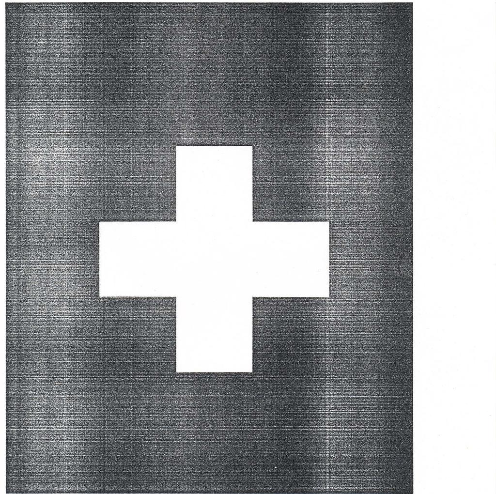
78
79 Primer Application Spin Coating Heated Vapor Coating The most popular - Wafer more - uniformity good - HMDS used reduced - Contamination less Spray Coating Dip Priming
80
81 Advantages of HMDS Not containing chlorine Not required hardbaking Adhesion promoter remains effective on a wafer more longer Pinhole and undercutting problem reduced Profile of resist increase
82 Positive Photoresist Developer Metal Ion Content Advantages - Higher development rate at exposure area - Better resist profile - Attack unexposed positive resist are less Disadvantages - Left residue - Cause contamination - Change device performance Metal Ion Free Advantages - Avoid from residue formation on wafer - Good for small geometry size Disadvantages - Attack unexposed positive photoresist - Low development rate - Poor resist profile
83 Why photoresist profile extremely important? - The structure of the layer underneath is depend on the structure of the resist. - Will change actual geometry size
84
85 Line And Space Definition i. Line a. Line is a bright field or the remain photoresist. b. To increase linewidth, decrease the exposure time or develop time. c. To decrease linewidth, increase the exposure time or develop time. ii. Space a. Space is a dark field or the area where the photoresist is removed after developed. b. To increase space width, increase the exposure time or develop time. c. To decrease space width, decrease the exposure time or develop time.
86 Lithography Process Control To control the lithography process is by measuring the critical dimension (CD) of the image Critical dimension the smallest dimension in the integrated circuit CD measurement consist of 3 steps - CD on mask - Cd on developed photoresist - Cd on patterned layer after etch
87
88
89
90 CONCLUSION Equipment - Exposure Tool - I line Stepper - Mask aligner - Wafer Track System - Vacuum Oven - Optical Microscope with CD Measurement - I line Positive Photoresist Lithography Process Specification Dehydration Bake Temp: 145 +/- 5 o C Vacuum: 10 mtorr Time: 15 minutes
91 Photoresist Coating Vapor Prime: HMDS Resist: I line +ve resist Velocity: 5000 rpm Time: 30 seconds Thickness: 1.2 um EBR: 1 mm Softbaking Temp: 90 +/- 1 o C Time: 60 seconds Align & Expose Tools: 1 line stepper & Mask aligner. Exp Energy: 200 mj / mm Exp Latitude: 20 MJ Focus Latitude: 4 um PE Baking Temp; 110 +/- 1 o C Time: 95 seconds Development Technique: Spray & Puddle Velocity: 4500 rpm Time; 60 seconds Hardbake Temp: 120 +/- 1 o C Time: 80 seconds CD Measurement Tolerance: 0.3 um
92 Photolithography Process Characterization
93 PHOTORESIST THICKNESS DETERMINATION Starting Material : Bare Si Wafer FSI Clean Dehydration Bake HMDS & Cooldown Wafer Resist Coating - Resist Type : PRH - Variable : Spin Speed - Constant : Others Softbake Resist Thickness Measurement - Ellipsometer or Nanospec Resist Thickness Determined - At Tentative Spin Speed
94 PHOTORESIST THICKNESS UNIFORMITY CHARACTERIZATION Starting Material Base Silicon Dehydration Bake HMDS & Cool Down Wafer Resist Coating Resist Type: PRH Constant : Spin Speed Variables : Dispense Volume Dispense Speed Dispense time Dispense spin speed Exhaust Flows Softbake Evaluation
95 Phase 1 Resist Thickness Uniformity Across wafer - Ellipsometer Wafer To Wafer - Ellipsometer PHOTORESIST THICKNESS UNIFORMITY DETERMINED
96 EXPERIMENTAL RESULT FORMAT FOR PHOTORESIST THICKNESS UNIFORMITY CHARACTERIZATION
97 PHOTORESIST THICKNESS UNIFORMITY & REPEATABILITY CHARACTERIZATION Starting Material Base Silicon Dehydration Bake HMDS & Cool Down Wafer Resist Coating Resist Type : RPH Constant : Spin Speed Variables : Dispense Volume Dispense Speed Dispense time Dispense spin speed Exhaust Flows Softbake Evaluation.
98 Phase 1 Resist Thickness Uniformity Across wafer - Ellipsometer Wafer To Wafer - Ellipsometer Phase 2 Resist Thickness Uniformity & Repeatability Across Wafer - Ellipsometer Wafer To Wafer - Ellipsometer Characterize Variables For Resist Thickness Uniformity And Repeatability Are Determined
99 Aim - PHOTORESIST CONTRAST ASSESSMENT To identify the best photoresist profile with a vertical sidewall Image Contrast - Different in density or optical gradient at image sidewall Parameters - Exposure energy & development time HIGH CONTRAST LOW CONTRAST
100 PHOTORESIST CONTRAST ASSESSMENT FLOW CHART Starting Material - Si Bare wafer with specific Resist thickness Softbake Align & Expose - Energy (E1) - Reticle : Test reticle (1.0 um resolution) Development - Time : Increase or decrease Repeat the whole process Hardbake - Adjust develop time PHOTORESIST PROFILE EVALUATION Cleave Wafer SEM Examination Photoresist profile _ Slope sidewall Photoresist Profile - Vertical Sidewall Exposure energy with vertical photoresist profile determined E1 + develop time, DS
101 EXPOSURE LEVEL DETERMINATION Starting Material Si wafer with photoresist Coated - Specific resist thickness - Equipment : stepper - Reticle : test reticle ( 1.0 um resolution ) Align & Expose wafer - Exposure matrix ( 30 Mj 300 mj in steps of 10 mj ) Development - Standard Parameters Energy level Evaluation Light Microscope ( Observe at 1.0 um resolution ) The tentative energy level at 1.0 um resolution is determined ( Eo )
102 Align & Expose Wafer - 5 different energy Align & Expose with Eo Align & Expose with Eo - 10 mj Align & Expose with Eo - 20 Mj Align & Expose with Eo + 10 mj Align & Expose with Eo + 20 mj Development Energy Level Evaluation Linewidth measurement ( 1.0 um resolution ) SEM The Best Energy Level Determined ( E1 )
103 EXPOSURE LATITUDE MEASUREMENT Starting Material - Bare SiWafer - photoresist thickness : Ao Softbake Align & Expose -Exposure Matrix - Energy : ( E1 n10mj ) & ( E1 + n10mj ) Development Hardbake EXPOSURE LATITUDE MEASUREMENT Wafer Cleaving SEM Examination EXPOSURE LATITUDE DETERMINED EMAX & Emin
104 EXAMPLE RESULT OF EXPOSURE LATITUDE DETERMINED Example typical result Let say E1 = 170 mj / cm 2 Exposure Energy ( mj / cm 2 ) Measurement ( um ) The exposure latitude for 1.00 um geometry size is 160 mj / cm 2 to 180 mj / cm 2 or 30 mj / cm 2.
105 FOCUS LATITUDE MEASUREMENT Starting Material - Bare Si Wafer Photoresist Thickness : Ao Softbake Align & Expose 1 - Reticle : Test reticle ( 1.0 um resolution ) - Focus level : The best ( Fo ) Align & Expose 2 - Reticle : Test reticle ( 1.0 um resolution ) - Focus level : Increase 4 steps focus in the steps of 1 um from Fo Align & Expose 3 - Reticle : Test reticle ( 1.0 um resolution ) - Focus level : Decrease 4 steps focus in the steps of 1 um from Fo Development
106 Hardbake FOCUS LATITUDE MEASUREMENT Wafer Cleaving SEM Examination - Linewidth Measurement ( 1.0 um resolution ) FOCUS LATITUDE DETERMINED + / - Fx um
107 Example result of focus latitude determination Focus Level ( um ) Linewidth Measurement ( um ) The focus latitude for 1.0 um geometry size is +/- 2 um or 4 um range. Focus latitude should be greater than photoresist thickness.
Photolithography I ( Part 2 )
") 1 Photolithography I ( Part 2 ) Chapter 13 : Semiconductor Manufacturing Technology by M. Quirk & J. Serda Bjørn-Ove Fimland, Department of Electronics and Telecommunication, Norwegian University of Science
1 Photolithography I ( Part 2 ) Chapter 13 : Semiconductor Manufacturing Technology by M. Quirk & J. Serda Bjørn-Ove Fimland, Department of Electronics and Telecommunication, Norwegian University of Science
Technical Data Sheet Technisches Datenblatt
 AZ ECI 3000 Photoresist Universal i-line/crossover Photoresist Series GENERAL INFORMATION AZ ECI 3000 photoresist series are a family of fast positive resists with high resolution capabilities (0.4 µm
Photoresist Coat, Expose and Develop Laboratory Dr. Lynn Fuller
 ROCHESTER INSTITUTE OF TECHNOLOGY MICROELECTRONIC ENGINEERING Photoresist Coat, Expose and Develop Laboratory Dr. Lynn Fuller Webpage: http://www.rit.edu/lffeee 82 Lomb Memorial Drive Rochester, NY 14623-5604
micro resist technology
 Characteristics Processing guidelines Negative Tone Photoresist Series ma-n 2400 ma-n 2400 is a negative tone photoresist series designed for the use in micro- and nanoelectronics. The resists are available
micro resist technology
 Characteristics Processing guidelines Negative Tone Photoresist Series ma-n 1400 ma-n 1400 is a negative tone photoresist series designed for the use in microelectronics and microsystems. The resists are
Processing guidelines. Negative Tone Photoresists mr-ebl 6000
 Characteristics Processing guidelines Negative Tone Photoresists mr-ebl 6000 mr-ebl 6000 is a chemically amplified negative tone photoresist for the use in micro- and nanoelectronics. - Electron beam sensitive
EE 527 MICROFABRICATION. Lecture 15 Tai-Chang Chen University of Washington EE-527 M4 MASK SET: NPN BJT. C (sub) A E = 40 µm x 40 µm
 A E = 40 µm x 40 µm") EE 527 MICROFABRICATION Lecture 15 Tai-Chang Chen University of Washington EE-527 M4 MASK SET: NPN BJT C (sub) E B A E = 40 µm x 40 µm 1 EE-527 M4 MASK SET: MOS C-V TEST CAPACITORS W = 10 µm L = 10 µm
EE 527 MICROFABRICATION Lecture 15 Tai-Chang Chen University of Washington EE-527 M4 MASK SET: NPN BJT C (sub) E B A E = 40 µm x 40 µm 1 EE-527 M4 MASK SET: MOS C-V TEST CAPACITORS W = 10 µm L = 10 µm
AZ BARLi II Solvent Compatible Bottom Antireflective Coating for i-line Process. Data Package
 AZ BARLi II Solvent Compatible Bottom Antireflective Coating for i-line Process Data Package AZ BARLi II Coating Material Features, Process, and Performance AZ s bottom antireflective coating material,
Major Fabrication Steps in MOS Process Flow
 Major Fabrication Steps in MOS Process Flow UV light Mask oxygen Silicon dioxide photoresist exposed photoresist oxide Silicon substrate Oxidation (Field oxide) Photoresist Coating Mask-Wafer Alignment
Processing guidelines. Negative Tone Photoresist Series ma-n 2400
 Characteristics Processing guidelines Negative Tone Photoresist Series ma-n 2400 ma-n 2400 is a negative tone photoresist series designed for the use in micro- and nanoelectronics. The resists are available
AZ BARLi II Solvent Compatible Bottom Antireflective Coating for i-line Process Data Package
 AZ BARLi II Solvent Compatible Bottom Antireflective Coating for i-line Process Data Package The information contained herein is, as far as we are aware, true and accurate. However, no representations
4. Thermal Oxidation. a) Equipment Atmospheric Furnace
 Equipment Atmospheric Furnace") 4. Thermal Oxidation a) Equipment Atmospheric Furnace Oxidation requires precise control of: temperature, T ambient gas, G time spent at any given T & G, t Vito Logiudice 34 4. Thermal Oxidation b) Mechanism
4. Thermal Oxidation a) Equipment Atmospheric Furnace Oxidation requires precise control of: temperature, T ambient gas, G time spent at any given T & G, t Vito Logiudice 34 4. Thermal Oxidation b) Mechanism
Processing guidelines
 Processing guidelines mr-uvcur21 series UV-curable Polymer for UV-based Nanoimprint Lithography Characteristics mr-uvcur21 is a liquid UV-curable polymer system with low viscosity and high curing rate
UV5 POSITIVE DUV PHOTORESIST For Microlithography Applications
 UV5 POSITIVE DUV PHOTORESIST For Microlithography Applications DESCRIPTION UV5 positive DUV photoresist has been optimized to provide vertical profile imaging of isolated and semidense features for device
P4000 Thick Film Photoresist
 D A T A S H E E T AZ Description AZ series photoresists provide unmatched capabilities in demanding applications requiring film thicknesses ranging from 3 to over 60 µm. These production proven photoresists
SU Permanent Epoxy Negative Photoresist PROCESSING GUIDELINES FOR:
 SU-8 2000 Permanent Epoxy Negative Photoresist PROCESSING GUIDELINES FOR: SU-8 2025, SU-8 2035, SU-8 2050 and SU-8 2075 SU-8 2000 is a high contrast, epoxy based photoresist designed for micromachining
Because of equipment availability, cost, and time, we will use aluminum as the top side conductor
 Because of equipment availability, cost, and time, we will use aluminum as the top side conductor Top Side Conductor vacuum deposition Aluminum sputter deposit in Argon plasma CVC 601-sputter deposition
UV5 POSITIVE DUV PHOTORESIST For DUV Applications
 UV5 POSITIVE DUV PHOTORESIST For DUV Applications DESCRIPTION UV5 positive DUV photo resist has been optimized to provide vertical profile imaging of isolated and semidense features for device production
SU Permanent Epoxy Negative Photoresist PROCESSING GUIDELINES FOR:
 SU-8 2000 Permanent Epoxy Negative Photoresist PROCESSING GUIDELINES FOR: SU-8 2000.5, SU-8 2002, SU-8 2005, SU-8 2007, SU-8 2010 and SU-8 2015 SU-8 2000 is a high contrast, epoxy based photoresist designed
UV6 POSITIVE DUV PHOTORESIST For DUV Applications
 UV6 POSITIVE DUV PHOTORESIST For DUV Applications DESCRIPTION UV6 Positive DUV Photoresist has been optimized to provide vertical profile imaging of dense and semi-isolated features for device production
SU Permanent Epoxy Negative Photoresist PROCESSING GUIDELINES FOR:
 SU-8 2000 Permanent Epoxy Negative Photoresist PROCESSING GUIDELINES FOR: SU-8 2100 and SU-8 2150 www.microchem.com SU-8 2000 is a high contrast, epoxy based photoresist designed for micromachining and
GLM General information. Technical Datasheet
 GLM 2060 Nanocomposite SU-8-negative tone photo-epoxy for layers from 6.0 to 50µm Technical Datasheet Gersteltec Sarl. Générale Guisan 26, 1009, Pully Switzerland Switzerland / Israel / Taiwan Contact:
Dow Corning WL-5150 Photodefinable Spin-On Silicone
 Dow Corning WL-515 Photodefinable Spin-On Silicone Properties and Processing Procedures Introduction Dow Corning WL-515 is a silicone formulation which can be photopatterned and cured using standard microelectronics
DuPont MX5000 Series
 DuPont MX5000 Series DATA SHEET & PROCESSING INFORMATION High Performance Multi-Purpose Polymer Film for MEMS Applications PRODUCT FEATURES/ APPLICATIONS Negative working, aqueous processable dry film
MCC. PMGI Resists NANO PMGI RESISTS OFFER RANGE OF PRODUCTS
 MCC PMGI RESISTS OFFER Sub.25µm lift-off processing Film thicknesses from 5µm Choice of resin blends for optimal undercut control High thermal stability Superior adhesion to Si, NiFe, GaAs, InP
Introduction to Lithography
 Introduction to Lithography G. D. Hutcheson, et al., Scientific American, 290, 76 (2004). Moore s Law Intel Co-Founder Gordon E. Moore Cramming More Components Onto Integrated Circuits Author: Gordon E.
Lab #2 Wafer Cleaning (RCA cleaning)
") Lab #2 Wafer Cleaning (RCA cleaning) RCA Cleaning System Used: Wet Bench 1, Bay1, Nanofabrication Center Chemicals Used: H 2 O : NH 4 OH : H 2 O 2 (5 : 1 : 1) H 2 O : HF (10 : 1) H 2 O : HCl : H 2 O 2
Lab #2 Wafer Cleaning (RCA cleaning) RCA Cleaning System Used: Wet Bench 1, Bay1, Nanofabrication Center Chemicals Used: H 2 O : NH 4 OH : H 2 O 2 (5 : 1 : 1) H 2 O : HF (10 : 1) H 2 O : HCl : H 2 O 2
MCC. LOR Lift-Off Resists LOR RESISTS OFFER TYPES OF RESISTS
 MCC LOR RESISTS OFFER Submicron linewidth control Finely tuned undercuts Does not intermix with imaging resists (no scum) Excellent adhesion to Si, NiFe, GaAs, InP and many other III-V and II-VI materials
125nXT Series. EMD PeRFoRmaNce MaTeRIaLs. technical datasheet. Photopolymer Negative Tone Photoresists APPLICATION TYPICAL PROCESS THICKNESS GRADES
 EMD PeRFoRmaNce MaTeRIaLs technical datasheet AZ 125nXT Series Photopolymer Negative Tone Photoresists APPLICATION Thick photopolymer photoresists featuring aspect ratios and photospeed not possible with
Fabrication Technology, Part I
 EEL5225: Principles of MEMS Transducers (Fall 2003) Fabrication Technology, Part I Agenda: Oxidation, layer deposition (last lecture) Lithography Pattern Transfer (etching) Impurity Doping Reading: Senturia,
CYCLOTENE* 4000 Series Advanced Electronic Resins (Photo BCB)
") Revised: February 2005 CYCLOTENE* 4000 Series Advanced Electronic Resins (Photo BCB) Processing Procedures for CYCLOTENE 4000 Series Photo BCB Resins DS2100 Puddle Develop Process 1. Introduction The CYCLOTENE
Revised: February 2005 CYCLOTENE* 4000 Series Advanced Electronic Resins (Photo BCB) Processing Procedures for CYCLOTENE 4000 Series Photo BCB Resins DS2100 Puddle Develop Process 1. Introduction The CYCLOTENE
Fabrication and Layout
 ECEN454 Digital Integrated Circuit Design Fabrication and Layout ECEN 454 3.1 A Glimpse at MOS Device Polysilicon Aluminum ECEN 475 4.2 1 Material Classification Insulators Glass, diamond, silicon oxide
Fabrication Process. Crystal Growth Doping Deposition Patterning Lithography Oxidation Ion Implementation CONCORDIA VLSI DESIGN LAB
 Fabrication Process Crystal Growth Doping Deposition Patterning Lithography Oxidation Ion Implementation 1 Fabrication- CMOS Process Starting Material Preparation 1. Produce Metallurgical Grade Silicon
1500 Series. EMD PeRFoRmaNce MaTeRIaLs. technical datasheet. Positive Tone Photoresists APPLICATION TYPICAL PROCESS. SPIN CURVES (150mm wafers)
") EMD PeRFoRmaNce MaTeRIaLs technical datasheet AZ 1500 Series Positive Tone Photoresists APPLICATION General purpose positive tone photoresists featuring excellent substrate adhesion for demanding wet etch
EMD PeRFoRmaNce MaTeRIaLs technical datasheet AZ 1500 Series Positive Tone Photoresists APPLICATION General purpose positive tone photoresists featuring excellent substrate adhesion for demanding wet etch
Introduction to Nanoscience and Nanotechnology
 Introduction to Nanoscience and Nanotechnology ENS 463 2. Principles of Nano-Lithography by Alexander M. Zaitsev alexander.zaitsev@csi.cuny.edu Tel: 718 982 2812 Office 4N101b 1 Lithographic patterning
Supporting Information: Model Based Design of a Microfluidic. Mixer Driven by Induced Charge Electroosmosis
 Supporting Information: Model Based Design of a Microfluidic Mixer Driven by Induced Charge Electroosmosis Cindy K. Harnett, Yehya M. Senousy, Katherine A. Dunphy-Guzman #, Jeremy Templeton * and Michael
EECS130 Integrated Circuit Devices
 EECS130 Integrated Circuit Devices Professor Ali Javey 9/13/2007 Fabrication Technology Lecture 1 Silicon Device Fabrication Technology Over 10 15 transistors (or 100,000 for every person in the world)
Photolithography. Dong-Il Dan Cho. Seoul National University Nano/Micro Systems & Controls Laboratory
 Lecture 9: Photolithography School of Electrical l Engineering i and Computer Science, Seoul National University Nano/Micro Systems & Controls Laboratory Email: dicho@snu.ac.kr URL: http://nml.snu.ac.kr
Microelectronic Device Instructional Laboratory. Table of Contents
 Introduction Process Overview Microelectronic Device Instructional Laboratory Introduction Description Flowchart MOSFET Development Process Description Process Steps Cleaning Solvent Cleaning Photo Lithography
ARC XL Series. Broadband g-line & i-line Anti-Reflective Coatings
 ARC XL Series Broadband g-line & i-line Anti-Reflective Coatings Why Use a Brewer Science ARC? Resist Resist Substrate ARC Substrate Without Brewer ARC With Brewer ARC Lithography Reflective Problems In
How To Write A Flowchart
 1 Learning Objectives To learn how you transfer a device concept into a process flow to fabricate the device in the EKL labs You learn the different components that makes up a flowchart; process blocks,
INTERVIA BPP-10 Photoresist
 Technical Data Sheet INTERVIA BPP-10 Photoresist For Advanced Packaging Applications Description Regional Product Availability Advantages INTERVIA BPP-10 Photoresist is a general-purpose, multi-wavelength
UV15: For Fabrication of Polymer Optical Waveguides
 CASE STUDY UV15: For Fabrication of Polymer Optical Waveguides Master Bond Inc. 154 Hobart Street, Hackensack, NJ 07601 USA Phone +1.201.343.8983 Fax +1.201.343.2132 main@masterbond.com CASE STUDY UV15:
BEFORE you can do any resist processing, you must be familiar with the chemicals you will be using, and know and respect the dangers of them.
 Overview Any e-beam exposure is highly dependant upon processing and the substrate. This information is provided as a starting point and will required experimentation to optimize things for your work.
More on VLSI Fabrication Technologies. Emanuele Baravelli
 More on VLSI Fabrication Technologies Emanuele Baravelli Some more details on: 1. VLSI meaning 2. p-si epitaxial layer 3. Lithography 4. Metallization 5. Process timings What does VLSI mean, by the way?
A discussion of crystal growth, lithography, etching, doping, and device structures is presented in
 Chapter 5 PROCESSING OF DEVICES A discussion of crystal growth, lithography, etching, doping, and device structures is presented in the following overview gures. SEMICONDUCTOR DEVICE PROCESSING: AN OVERVIEW
ACS300 Gen2. The coat develop solution from pilot to high volume production
 ACS300 Gen2 The coat develop solution from pilot to high volume production ACS300 Gen2 The Powerful Coating Solution for 300 mm features and benefits + + Highly flexible resist processing cluster for high-volume
Fabrication Technology
 Fabrication Technology By B.G.Balagangadhar Department of Electronics and Communication Ghousia College of Engineering, Ramanagaram 1 OUTLINE Introduction Why Silicon The purity of Silicon Czochralski
The Physical Structure (NMOS)
") The Physical Structure (NMOS) Al SiO2 Field Oxide Gate oxide S n+ Polysilicon Gate Al SiO2 SiO2 D n+ L channel P Substrate Field Oxide contact Metal (S) n+ (G) L W n+ (D) Poly 1 3D Perspective 2 3 Fabrication
The Physical Structure (NMOS) Al SiO2 Field Oxide Gate oxide S n+ Polysilicon Gate Al SiO2 SiO2 D n+ L channel P Substrate Field Oxide contact Metal (S) n+ (G) L W n+ (D) Poly 1 3D Perspective 2 3 Fabrication
TECHNICAL DATA SHEET DESCRIPTION PHYSICAL CHARACTERISTICS PRODUCT CHARACTERISTICS ETERTEC PR8200Y1 PHOTO-IMAGEABLE COVERLAY
 TECHNICAL DATA SHEET ETERTEC PR8200Y1 PHOTO-IMAGEABLE COVERLAY DESCRIPTION ETERTEC PR8200Y1 is an alkaline processable dry film photopolymer permanent photoresist utilising epoxy chemistry materials well
Chapter 3 Silicon Device Fabrication Technology
 Chapter 3 Silicon Device Fabrication Technology Over 10 15 transistors (or 100,000 for every person in the world) are manufactured every year. VLSI (Very Large Scale Integration) ULSI (Ultra Large Scale
Basic&Laboratory& Materials&Science&and&Engineering& Micro&Electromechanical&Systems&& (MEMS)&
&") Basic&Laboratory& Materials&Science&and&Engineering& Micro&Electromechanical&Systems&& (MEMS)& M105& As of: 27.10.2011 1 Introduction... 2 2 Materials used in MEMS fabrication... 2 3 MEMS fabrication processes...
Basic&Laboratory& Materials&Science&and&Engineering& Micro&Electromechanical&Systems&& (MEMS)& M105& As of: 27.10.2011 1 Introduction... 2 2 Materials used in MEMS fabrication... 2 3 MEMS fabrication processes...
Microfabrication of Integrated Circuits
 Microfabrication of Integrated Circuits OUTLINE History Basic Processes Implant; Oxidation; Photolithography; Masks Layout and Process Flow Device Cross Section Evolution Lecture 38, 12/05/05 Reading This
Bulk MEMS Fabrication Details Dr. Lynn Fuller, Casey Gonta, Patsy Cadareanu
 ROCHESTER INSTITUTE OF TECHNOLOGY MICROELECTRONIC ENGINEERING Bulk MEMS Fabrication Details Dr. Lynn Fuller, Casey Gonta, Patsy Cadareanu Webpage: http://people.rit.edu/lffeee 82 Lomb Memorial Drive Rochester,
Schematic creation of MOS field effect transistor.
 Schematic creation of MOS field effect transistor. Gate electrode Drain electrode Source electrode Gate oxide Gate length Page 1 Step 0 The positively doped silicon wafer is first coated with an insulating
EE 5344 Introduction to MEMS. CHAPTER 3 Conventional Si Processing
 3. Conventional licon Processing Micromachining, Microfabrication. EE 5344 Introduction to MEMS CHAPTER 3 Conventional Processing Why silicon? Abundant, cheap, easy to process. licon planar Integrated
Micro- and Nano-Technology... for Optics
 Micro- and Nano-Technology...... for Optics 3.2 Lithography U.D. Zeitner Fraunhofer Institut für Angewandte Optik und Feinmechanik Jena Electron Beam Column electron gun beam on/of control magnetic deflection
Complexity of IC Metallization. Early 21 st Century IC Technology
 EECS 42 Introduction to Digital Electronics Lecture # 25 Microfabrication Handout of This Lecture. Today: how are Integrated Circuits made? Silicon wafers Oxide formation by growth or deposition Other
TI 35ES image reversal resist
 MicroChemicals TI 35ES technical data sheet revised 10/2003 p. 1 of 11 TI 35ES image reversal resist Technical Data Sheet revised 10/2003 General Information MicroChemicals GmbH Schillerstrasse 18 D-89077
Czochralski Crystal Growth
 Czochralski Crystal Growth Crystal Pulling Crystal Ingots Shaping and Polishing 300 mm wafer 1 2 Advantage of larger diameter wafers Wafer area larger Chip area larger 3 4 Large-Diameter Wafer Handling
The Pennsylvania State University. The Graduate School. Department of Electrical Engineering DEPOSITION OF PATTERN TRANSFER MATERIALS BY THE MISTED
 The Pennsylvania State University The Graduate School Department of Electrical Engineering DEPOSITION OF PATTERN TRANSFER MATERIALS BY THE MISTED CHEMICAL DEPOSITION PROCESS A Thesis in Electrical Engineering
Chapter 3 CMOS processing technology
 Chapter 3 CMOS processing technology (How to make a CMOS?) Si + impurity acceptors(p-type) donors (n-type) p-type + n-type => pn junction (I-V) 3.1.1 (Wafer) Wafer = A disk of silicon (0.25 mm - 1 mm thick),
Lecture 19 Microfabrication 4/1/03 Prof. Andy Neureuther
 EECS 40 Spring 2003 Lecture 19 Microfabrication 4/1/03 Prof. ndy Neureuther How are Integrated Circuits made? Silicon wafers Oxide formation by growth or deposition Other films Pattern transfer by lithography
MCC. NANO PMMA and Copolymer
 MCC PRODUCT ATTRIBUTES NANO and Submicron linewidth control (polymethyl methacrylate) is a versatile polymeric material that is well suited Sub 0.1µm imaging for many imaging and non-imaging microelectronic
MEMS Surface Fabrication
 ROCHESTER INSTITUTE OF TECHNOLOGY MICROELECTRONIC ENGINEERING MEMS Surface Fabrication Dr. Lynn Fuller webpage: http://people.rit.edu/lffeee Electrical and Microelectronic Engineering Rochester Institute
In-situ Metrology for Deep Ultraviolet Lithography Process Control
 In-situ Metrology for Deep Ultraviolet Lithography Process Control Nickhil Jakatdar 1, Xinhui Niu, John Musacchio, Costas J. Spanos Dept. of Electrical Engineering and Computer Sciences, University of
ELEC 3908, Physical Electronics, Lecture 4. Basic Integrated Circuit Processing
 ELEC 3908, Physical Electronics, Lecture 4 Basic Integrated Circuit Processing Lecture Outline Details of the physical structure of devices will be very important in developing models for electrical behavior
EE40 Lec 22. IC Fabrication Technology. Prof. Nathan Cheung 11/19/2009
 Suggested Reading EE40 Lec 22 IC Fabrication Technology Prof. Nathan Cheung 11/19/2009 300mm Fab Tour http://www-03.ibm.com/technology/manufacturing/technology_tour_300mm_foundry.html Overview of IC Technology
Silicon Manufacturing
 Silicon Manufacturing Group Members Young Soon Song Nghia Nguyen Kei Wong Eyad Fanous Hanna Kim Steven Hsu th Fundamental Processing Steps 1.Silicon Manufacturing a) Czochralski method. b) Wafer Manufacturing
Processing Procedures for CYCLOTENE 3000 Series Dry Etch Resins
 Revised: April 2008 Processing Procedures for CYCLOTENE 3000 Series Dry Etch Resins 1. INTRODUCTION The CYCLOTENE 3000 series Advanced Electronic Resins derived from B-staged bisbenzocyclobutene (BCB)
Hybrid BARC approaches for FEOL and BEOL integration
 Hybrid BARC approaches for FEOL and BEOL integration Willie Perez a, Stephen Turner a, Nick Brakensiek a, Lynne Mills b, Larry Wilson b, Paul Popa b a Brewer Science, Inc., 241 Brewer Dr., Rolla, MO 6541
Temperature Scales. Questions. Temperature Conversions 7/21/2010. EE580 Solar Cells Todd J. Kaiser. Thermally Activated Processes
 7/1/010 EE80 Solar Cells Todd J. Kaiser Flow of Wafer in Fabrication Lecture 0 Microfabrication A combination of Applied Chemistry, Physics and ptics Thermal Processes Diffusion & xidation Photolithograpy
North America Europe, Middle East and Africa Latin America Asia-Pacific. Table 1. Photo-BCB Formulations
 Processing Procedures CYCLOTENE 4000 Series Advanced Electronics Resins (Photo BCB) Processing Procedures for CYCLOTENE 4000 Series Photo BCB Resins DS2100 Puddle Develop Process Regional Product Availability
Supporting Information
 Supporting Information The adhesion circle: A new approach to better characterize directional gecko-inspired dry adhesives Yue Wang, Samuel Lehmann, Jinyou Shao and Dan Sameoto* Department of Mechanical
Report 1. B. Starting Wafer Specs Number: 10 Total, 6 Device and 4 Test wafers
 Aaron Pederson EE 432 Lab Dr. Meng Lu netid: abp250 Lab instructor: Yunfei Zhao Report 1 A. Overview The goal of this lab is to go through the semiconductor fabrication process from start to finish. This
ECE 440 Lecture 27 : Equilibrium P-N Junctions I Class Outline:
 ECE 440 Lecture 27 : Equilibrium P-N Junctions I Class Outline: Fabrication of p-n junctions Contact Potential Things you should know when you leave Key Questions What are the necessary steps to fabricate
AZ P4620 Photoresist Data Package
 AZ P4620 Photoresist Data Package The information contained herein is, as far as we are aware, true and accurate. However, no representations or warranties, either express or implied, whether of merchantable
CYCLOTENE* 3000 Series Advanced Electronic Resins
 CYCLOTENE* 3000 Series Advanced Electronic Resins Revised: February 2005 Processing Procedures for CYCLOTENE 3000 Series Dry Etch Resins 1. INTRODUCTION The CYCLOTENE 3000 series advance electronic resins
Understanding. Brewer Science
 Understanding ARC Products General ARC Presentation: Slide #1 Overview Anti-reflective coating introduction Types of anti-reflective coating Advantages to anti-reflective coatings Advantages to bottom
PCHROME SPRAYING INSTRUCTIONS
 PCHROME SPRAYING INSTRUCTIONS FOR DECORATIVE APPLICATIONS While the coating instructions must be carefully followed to achieve a optimum result, the process is not limited to the treatment of one article
Avatrel Stress Buffer Coatings: Low Stress Passivation and Redistribution Applications
 Avatrel Stress Buffer Coatings: Low Stress Passivation and Redistribution Applications Ed Elce, Chris Apanius, Jeff Krotine, Jim Sperk, Andrew Bell, Rob Shick* Sue Bidstrup-Allen, Paul Kohl Takashi Hirano,
A Deep Silicon RIE Primer Bosch Etching of Deep Structures in Silicon
 A Deep Silicon RIE Primer Bosch Etching of Deep Structures in Silicon April 2009 A Deep Silicon RIE Primer 1.0) Etching: Silicon does not naturally etch anisotropically in fluorine based chemistries. Si
UVIII POSITIVE DUV PHOTO RESISTS
 UVIII POSITIVE DUV PHOTO RESISTS UVIII POSITIVE DUV PHOTO RESIST is optimized to provide wide process latitude for
FABRICATION OF CMOS INTEGRATED CIRCUITS. Dr. Mohammed M. Farag
 FABRICATION OF CMOS INTEGRATED CIRCUITS Dr. Mohammed M. Farag Outline Overview of CMOS Fabrication Processes The CMOS Fabrication Process Flow Design Rules EE 432 VLSI Modeling and Design 2 CMOS Fabrication
Lithography Tool Package
 4. Development Thomas Anhøj and Tine Greibe Outline 1. Introduction Process steps in UV lithography 2. Spin coating Resist composition Pre-treatment Principle Softbake Spin curve 3. Exposure Hardware Process
Semiconductor Technology
 Semiconductor Technology from A to Z Oxidation www.halbleiter.org Contents Contents List of Figures List of Tables II III 1 Oxidation 1 1.1 Overview..................................... 1 1.1.1 Application...............................
3.155J / 6.152J Micro/Nano Processing Technology TAKE-HOME QUIZ FALL TERM 2005
 3.155J / 6.152J Micro/Nano Processing Technology TAKE-HOME QUIZ FALL TERM 2005 1) This is an open book, take-home quiz. You are not to consult with other class members or anyone else. You may discuss the
Mostafa Soliman, Ph.D. May 5 th 2014
 Mostafa Soliman, Ph.D. May 5 th 2014 Mostafa Soliman, Ph.D. 1 Basic MEMS Processes Front-End Processes Back-End Processes 2 Mostafa Soliman, Ph.D. Wafers Deposition Lithography Etch Chips 1- Si Substrate
2015 EE410-LOCOS 0.5µm Poly CMOS Process Run Card Lot ID:
 STEP 0.00 - PHOTOMASK #0- ZERO LEVEL MARKS Starting materials is n-type silicon (5-10 ohm-cm). Add four test wafers labeled T1-T4. T1 and T2 will travel with the device wafers and get all of the processing
Microelectronics. Integrated circuits. Introduction to the IC technology M.Rencz 11 September, Expected decrease in line width
 Microelectronics Introduction to the IC technology M.Rencz 11 September, 2002 9/16/02 1/37 Integrated circuits Development is controlled by the roadmaps. Self-fulfilling predictions for the tendencies
the surface of a wafer, usually silicone. In this process, an oxidizing agent diffuses into the wafer
 Analysis of Oxide Thickness Measurement Techniques of SiO2: Nanometrics Nanospec Reflectometer and Color Chart Eman Mousa Alhajji North Carolina State University Department of Materials Science and Engineering
NANOMETER AND HIGH ASPECT RATIO PATTERNING BY ELECTRON BEAM LITHOGRAPHY USING A SIMPLE DUV NEGATIVE TONE RESIST
 NANOMETER AND HIGH ASPECT RATIO PATTERNING BY ELECTRON BEAM LITHOGRAPHY USING A SIMPLE DUV NEGATIVE TONE RESIST H. Elsner and H.-G. Meyer Institute for Physical High Technology (IPHT), Dept. of Cryoelectronics,
Technology process. It s very small world. Electronics and Microelectronics AE4B34EM. Why is the integration so beneficial?
 It s very small world Electronics and Microelectronics AE4B34EM 9. lecture IC processing technology Wafer fabrication Lithography How to get 1 000 000 000 Components to 1 cm 2 Human hair on the surface
XV750 Imageline Etch Resist Family
 XV750 Imageline Etch Resist Family Imageline XV750 etch resist is a liquid photoimageable product, which dries by evaporation to give a film that can be sensitized by exposure to UV wavelengths between
Single-digit-resolution nanopatterning with. extreme ultraviolet light for the 2.5 nm. technology node and beyond
 Electronic Supplementary Material (ESI) for Nanoscale. This journal is The Royal Society of Chemistry 205 Supplementary Information for: Single-digit-resolution nanopatterning with extreme ultraviolet
Illuminating Innovations
 Illuminating Innovations TM Silicone Solutions for LED Packaging Emir Debastiani Application Engineer Dow Corning Brazil Email: emir.debastiani@dowcorning.com Table of Contents Dow Corning Introduction
3.155J / 6.152J MICROELECTRONICS PROCESSING TECHNOLOGY TAKE-HOME QUIZ FALL TERM 2003
 3.155J / 6.152J MICROELECTRONICS PROCESSING TECHNOLOGY TAKE-HOME QUIZ FALL TERM 2003 1) This is an open book, take-home quiz. You are not to consult with other class members or anyone else. You may discuss
All fabrication was performed on Si wafers with 285 nm of thermally grown oxide to
 Supporting Information: Substrate preparation and SLG growth: All fabrication was performed on Si wafers with 285 nm of thermally grown oxide to aid in visual inspection of the graphene samples. Prior