Polymer-based Microfabrication
|
|
|
- Dulcie Clarke
- 5 years ago
- Views:
Transcription
1 Polymer-based Microfabrication PDMS SU-8 PMMA Hydrogel 1

 as a substrate,")


2 Soft Lithography Developed by Whitesides, et. al A set of techniques for microfabrication based on the use of lithography, soft substrate materials (PDMS) as a substrate, and molding of polymers Simple and cheap fabrication Rapid process for prototyping Micromolding Microtransfer molding Replica molding Microcontact Printing Monolayer (protein, cells.etc) 2
3 Micromolding Lithographyh (e.g. SU-8) Soft materials (PDMS) Molding Why micromolding? 3
4 Microcontact Printing Printing on a planar substrate with a rolling stamp Printing on a planar substrate with a planar PDMS stamp Print and pattern a layer of molecules Print and pattern probes on microarray Printing on a curved substrate with a planar stamp 4

5 Microtransfer molding (µtm) 5
6 Micromolding in Capillaries (MIMIC) 6


7 Solvent Assisted Micromolding (SAMIM) PDMS mold is wetted a solvent that can swell the polymer Solvent swells/dissolves a thin layer of polymer The resulting fluid (gellike Polymer/solvent) conforms the mold pattern Solvent evaporates and pattern solidifies Polystyrene, etc. solvent 7
8 Technical Problems in Soft Lithography Pairing Occurs at high aspect ratio Caused by weight and surface tension Occurs at low aspect ratio Caused by compression force while inking Sagging Shrinking during curing Swelling by nonpolar solvents Shrinking / swelling 8

9 PDMS (Polydimethylsiloxane) Deforms reversibly Can be molded with high fidelity Optically transparent down to ~300nm Durable and chemically inert Non-toxic Inexpensive Upon treatment in oxygen plasma, PDMS seals to itself, glass, silicon, silicon nitride, and some plastic materials 9
10 Rapid Prototyping Procedure for Soft-lithography 10
 Lithography SU-8 is a negative")


11 Thick Resist (e.g. Su-8) Lithography SU-8 is a negative photoresist based on EPON SU-8 epoxy resin for the near-uv wavelengths from 365 nm to 436 nm. At these wavelengths the photoresist has very low optical absorption, which makes photolithography of thick films with high aspect ratios possible. 1 St(Stroke)= 1 cm 2 s -1 11


12 Steps Spin speed: C nm C Baking times (min) : C (Microchem, Inc.) 12


13 PMMA (Poly methyl methacrylate) Dot pattern imprinted into PMMA ( polymethymethacrylate ). The dots have a 25 nm diameter and 120 nm period (Renstrom) Ti/Au dot pattern on a silicon substrate fabricated using nano-imprinting and a lift-off process. The dots have a 25 nm diameter and 120 nm period 13
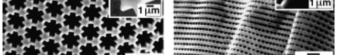
14 Hydrogel Based Microfabrication Hydrogel Fabrication Photosensitive (polarity like negative PR) Liquid-phase photo-polymerization Laminar flow-aided patterning Functional (stimuli-responsive) and non-functional materials Fabrication of fluidic channels, actuators, valves, pumps Typical polymerization time: 5-40 sec (UV light) Minimal Total fabrication time of a system ( <10 min) A hydrogel jacket valve in a T channel (D. Beebe) 14
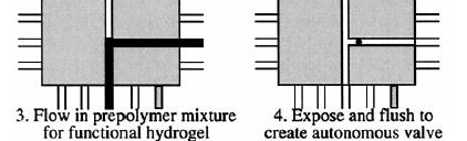
15 Fabrication of a valve in a Hydrogel Microchannel 2-D and 3-D micro fluidic network 15
16 Geometry Control during Fabrication by Using Laminar Flows 16
17 Rigid Materials vs. Soft (Elastomeric) Materials Rigid id materials Crystalline silicon, amorphous silicon, glass, quartz, metals Advantages: Fabrication process is mature and well developed Bulk-etching for forming two- and three-dimensional shapes Batch process compatible with IC process Silicon dioxide: good quality, stable chemically and thermally Disadvantages: Expensive Brittle Opaque (for silicon) in the UV/Vis regions Low dielectric strength (Si) Surface chemistry is difficult to manipulate Packaging/Bonding: Anodic bonding Fusion bonding Polymer bonding Good and Bad!! 17
18 Rigid Materials vs. Soft (Elastomeric) Materials Soft materials PDMS, PMMA, Polyimide, Hydrogel, etc.. Advantages: Quick Inexpensive Flexible (for actuation such as valuing) Transparent to visible/uv Durable and chemical insert Surface property easily modified Improved biocompatibility and bioactivity Disadvantages: Limited to simple structure Low thermal stability Low thermal and electrical conductivity Techniques for microfabrication not as well developed Packaging/Bonding: Through surface modification easy but not robust 18
Soft Lithography. Jin-Goo Park. Materials and Chemical Engineering Hanyang University, Ansan. Electronic Materials and Processing Lab.
 Hanyang University Soft Lithography Jin-Goo Park Materials and Chemical Engineering Hanyang University, Ansan Electronic Materials and Processing Lab. Introduction to Soft Lithography Research Micro- Electro-
Introduction to Micro/Nano Fabrication Techniques. Date: 2015/05/22 Dr. Yi-Chung Tung. Fabrication of Nanomaterials
 Introduction to Micro/Nano Fabrication Techniques Date: 2015/05/22 Dr. Yi-Chung Tung Fabrication of Nanomaterials Top-Down Approach Begin with bulk materials that are reduced into nanoscale materials Ex:
Soft Lithography: MIMIC. Micro Contact Printing. Microtransfer Molding. Soft Lithography: Replica Molding. Soft Lithography.
 Can We Measure Everything? Microfabrication Using Polymers Dr. Bruce K. Gale ENGR 494C and 594C Polymers for Microfabrication Examples diverse PDMS PMMA Polyurethane Polyimide Polystyrene Disadvantages
Alternative MicroFabrication and Applications in Medicine and Biology
 Alternative MicroFabrication and Applications in Medicine and Biology Massachusetts Institute of Technology 6.152 - Lecture 15 Fall 2003 These slides prepared by Dr. Hang Lu Outline of Today s Materials
Introduction to MEMS
 Introduction to MEMS 520.487 Lecture Outline 1. Photolithography 2. Thermal Oxidation 3. Wet Etching 4. Dry Etching 5. Unconventional Microfabrication Photolithography Conventional Photoresists Typically
Micro Fabrication : Soft Lithography
 Micro Fabrication : Soft Lithography Last Class: 1. Electrowetting on Dielectric (EWOD) 2. Setup in EWOD 3. Basic Manipulations : Mixing Splitting, Translation 4. Optoelectrowetting (OEW) Today s Contents:
Module 13: Soft Lithography. Lecture 19: Soft Lithography 2
 Module 13: Soft Lithography Lecture 19: Soft Lithography 2 1 In the previous lecture we have introduced the concept of Soft Lithography and discussed three of the methods, which are Replica Molding, Micro
Lecture 10 Part II: Micro f b a i ca i tion for Microfluidics Microfluidics and aand Microfluidics Devices
 Lecture 10 Part II: Microfabrication i for Microfluidics and Microfluidics Devices Silicon Etching Polymer-based Micromachining Assembly and Packaging Biocompartibility Techniques involved: Wet etching
Advanced Polymers And Resists For Nanoimprint Lithography
 Q U A L I T Y A S S U R A N C E MICROSYSTEMS & NANOSYSTEMS SPECIAL REPORT Advanced Polymers And Resists For Nanoimprint Lithography Numerous polymer systems specifically designed for nanoimprint lithography
EE 5344 Introduction to MEMS. CHAPTER 3 Conventional Si Processing
 3. Conventional licon Processing Micromachining, Microfabrication. EE 5344 Introduction to MEMS CHAPTER 3 Conventional Processing Why silicon? Abundant, cheap, easy to process. licon planar Integrated
Photolithography. Dong-Il Dan Cho. Seoul National University Nano/Micro Systems & Controls Laboratory
 Lecture 9: Photolithography School of Electrical l Engineering i and Computer Science, Seoul National University Nano/Micro Systems & Controls Laboratory Email: dicho@snu.ac.kr URL: http://nml.snu.ac.kr
Module 12: Nano Imprint Lithography. Lecture 16: Nano Imprint Lithography 1
 Module 12: Nano Imprint Lithography Lecture 16: Nano Imprint Lithography 1 1 In the previous five lectures (Lectures 11 to 15) we have seen how Photolithography can be used for patterning, particularly
UV15: For Fabrication of Polymer Optical Waveguides
 CASE STUDY UV15: For Fabrication of Polymer Optical Waveguides Master Bond Inc. 154 Hobart Street, Hackensack, NJ 07601 USA Phone +1.201.343.8983 Fax +1.201.343.2132 main@masterbond.com CASE STUDY UV15:
Chapter 5 Polymer Micromachining
 Chapter 5 Polymer Micromachining 5.1 Thick Resist Lithography 5.1.1 Polymethylmethacrylate (PMMA) resist (1)PMMA was originally used as a resist material for the LIGA technique Substrate Metal Seed layer
Soft Fabrication and Polymers
 Introduction to BioMEMS & Medical Microdevices Soft Fabrication and Polymers Companion lecture to the textbook: Fundamentals of BioMEMS and Medical Microdevices, by Prof., http://saliterman.umn.edu/ R012408
Nanoimprinting in Polymers and Applications in Cell Studies. Albert F. YEE Chemical Engineering & Materials Science UC Irvine
 Nanoimprinting in Polymers and Applications in Cell Studies Albert F. YEE Chemical Engineering & Materials Science UC Irvine Presentation outline Motivation Reversal imprinting Soft inkpad imprinting on
Preface Preface to First Edition
 Contents Foreword Preface Preface to First Edition xiii xv xix CHAPTER 1 MEMS: A Technology from Lilliput 1 The Promise of Technology 1 What Are MEMS or MST? 2 What Is Micromachining? 3 Applications and
Surface Micromachining
 Surface Micromachining Outline Introduction Material often used in surface micromachining Material selection criteria in surface micromachining Case study: Fabrication of electrostatic motor Major issues
The Effect of Hydrophobic Patterning on Micromolding of Aqueous-Derived Silk Structures
 The Effect of Hydrophobic Patterning on Micromolding of Aqueous-Derived Silk Structures Konstantinos Tsioris 1, Robert D White 1, David L Kaplan 2, and Peter Y Wong 1 1 Mechanical Engineering, Tufts University,
Lecture 6. Through-Wafer Interconnect. Agenda: Through-wafer Interconnect Polymer MEMS. Through-Wafer Interconnect -1. Through-Wafer Interconnect -2
 Agenda: EEL6935 Advanced MEMS (Spring 2005) Instructor: Dr. Huikai Xie Lecture 6 Through-wafer Interconnect EEL6935 Advanced MEMS 2005 H. Xie 1/21/2005 1 Motivations: Wafer-level packaging CMOS 3D Integration
3. Overview of Microfabrication Techniques
 3. Overview of Microfabrication Techniques The Si revolution First Transistor Bell Labs (1947) Si integrated circuits Texas Instruments (~1960) Modern ICs More? Check out: http://www.pbs.org/transistor/background1/events/miraclemo.html
Introduction to Microfabrication Techniques
 Introduction to Microfabrication Techniques 5 2 Introduction to Microfabrication Techniques Rabih Zaouk, Benjamin Y. Park, and Marc J. Madou Summary The advent of photolithography literally brought about
Thermal Nanoimprinting Basics
 Thermal Nanoimprinting Basics Nanoimprinting is a way to replicate nanoscale features on one surface into another, like stamping copies are made by traditional fabrication techniques (optical/ebeam lith)
NanoSystemsEngineering: NanoNose Final Status, March 2011
 1 NanoSystemsEngineering: NanoNose Final Status, March 2011 The Nanonose project is based on four research projects (VCSELs, 3D nanolithography, coatings and system integration). Below, the major achievements
Fabrication of Microchannel and Micro Chamber for Microfluidic Lab-on-Chip
 Australian Journal of Basic and Applied Sciences, 7(1): 166-170, 2013 ISSN 1991-8178 Fabrication of Microchannel and Micro Chamber for Microfluidic Lab-on-Chip 1 U. Hashim, 1 Tijjani Adam and 2 Peter Ling
Wireless implantable chip with integrated Nitinol-based pump for radio-controlled local drug delivery
 Electronic Supplementary Material (ESI) for Lab on a Chip. This journal is The Royal Society of Chemistry 2014 Electronic Supplementary Information Wireless implantable chip with integrated Nitinol-based
Simple UV-based Soft-lithography Process for. Fabrication of Low-Loss Polymer PSQ-L-based. Waveguides
 Simple UV-based Soft-lithography Process for Fabrication of Low-Loss Polymer PSQ-L-based Waveguides Jie Teng 1, 2, 4, Stijn Scheerlinck 4, Geert Morthier 4, Roel Baets 4, Hongbo Zhang 2,3, Xigao Jian 2,3,
Photolithography I ( Part 2 )
") 1 Photolithography I ( Part 2 ) Chapter 13 : Semiconductor Manufacturing Technology by M. Quirk & J. Serda Bjørn-Ove Fimland, Department of Electronics and Telecommunication, Norwegian University of Science
1 Photolithography I ( Part 2 ) Chapter 13 : Semiconductor Manufacturing Technology by M. Quirk & J. Serda Bjørn-Ove Fimland, Department of Electronics and Telecommunication, Norwegian University of Science
Cell-Environment Interactions. Chieh-Chun Chen
 Cell-Environment Interactions Chieh-Chun Chen Part 1: Soft Lithography in Biology and Biochemistry Chieh-Chun Chen Outlines Introduction Key features of soft lithography Applications In microscopic biochemical
Surface Micromachining
 Surface Micromachining Micro Actuators, Sensors, Systems Group University of Illinois at Urbana-Champaign Outline Definition of surface micromachining Most common surface micromachining materials - polysilicon
Supporting Information: Model Based Design of a Microfluidic. Mixer Driven by Induced Charge Electroosmosis
 Supporting Information: Model Based Design of a Microfluidic Mixer Driven by Induced Charge Electroosmosis Cindy K. Harnett, Yehya M. Senousy, Katherine A. Dunphy-Guzman #, Jeremy Templeton * and Michael
General Introduction to Microstructure Technology p. 1 What is Microstructure Technology? p. 1 From Microstructure Technology to Microsystems
 General Introduction to Microstructure Technology p. 1 What is Microstructure Technology? p. 1 From Microstructure Technology to Microsystems Technology p. 9 The Parallels to Microelectronics p. 15 The
Silicon and Non-Silicon Materials for BioMEMS Fabrication
 Silicon and Non-Silicon Materials for BioMEMS Fabrication M. Gheorghe, M. Dinca, P. Galvin* * Tyndall National Institute, Cork, Ireland maringhe@tyndall.ie Short presentation of the Tyndall National Institute,
Fully-integrated, Bezel-less Transistor Arrays Using Reversibly Foldable Interconnects and Stretchable Origami Substrates
 Electronic Supplementary Material (ESI) for Nanoscale. This journal is The Royal Society of Chemistry 2016 Fully-integrated, Bezel-less Transistor Arrays Using Reversibly Foldable Interconnects and Stretchable
Manipulation and control of spatial ALD layers for flexible devices. Aimcal Memphis 2016; Edward Clerkx
 Manipulation and control of spatial ALD layers for flexible devices Meyer Burger Netherlands Equipment manufacturer Functional inkjet printing Based in Eindhoven, the Netherlands Part of world-wide Meyer
EECS130 Integrated Circuit Devices
 EECS130 Integrated Circuit Devices Professor Ali Javey 9/13/2007 Fabrication Technology Lecture 1 Silicon Device Fabrication Technology Over 10 15 transistors (or 100,000 for every person in the world)
Fabrication of Embedded Microvalve on PMMA Microfluidic Devices through Surface Functionalization
 Fabrication of Embedded Microvalve on PMMA Microfluidic Devices through Surface Functionalization A. G. G. Toh, Z.F. Wang and S.H. Ng Singapore Institute of Manufacturing Technology Abstract- The integration
Photoresist Coat, Expose and Develop Laboratory Dr. Lynn Fuller
 ROCHESTER INSTITUTE OF TECHNOLOGY MICROELECTRONIC ENGINEERING Photoresist Coat, Expose and Develop Laboratory Dr. Lynn Fuller Webpage: http://www.rit.edu/lffeee 82 Lomb Memorial Drive Rochester, NY 14623-5604
Chapter 2 Manufacturing Process
 Digital Integrated Circuits A Design Perspective Chapter 2 Manufacturing Process 1 CMOS Process 2 CMOS Process (n-well) Both NMOS and PMOS must be built in the same silicon material. PMOS in n-well NMOS
Processing guidelines. Negative Tone Photoresists mr-ebl 6000
 Characteristics Processing guidelines Negative Tone Photoresists mr-ebl 6000 mr-ebl 6000 is a chemically amplified negative tone photoresist for the use in micro- and nanoelectronics. - Electron beam sensitive
Introduction to Nanoscience and Nanotechnology
 Introduction to Nanoscience and Nanotechnology ENS 463 2. Principles of Nano-Lithography by Alexander M. Zaitsev alexander.zaitsev@csi.cuny.edu Tel: 718 982 2812 Office 4N101b 1 Lithographic patterning
Czochralski Crystal Growth
 Czochralski Crystal Growth Crystal Pulling Crystal Ingots Shaping and Polishing 300 mm wafer 1 2 Advantage of larger diameter wafers Wafer area larger Chip area larger 3 4 Large-Diameter Wafer Handling
Supporting Information for. Conjugated polymer composite artificial muscle with solvent-induced anisotropic mechanical actuation
 Electronic Supplementary Material (ESI) for Journal of Materials Chemistry A. This journal is The Royal Society of Chemistry 2014 Supporting Information for Conjugated polymer composite artificial muscle
Three-dimensional SU-8 structures by reversal UV imprint
 Three-dimensional SU-8 structures by reversal UV imprint W. Hu, a B. Yang, C. Peng, and S. W. Pang b Solid State Electronics Laboratory, Department of Electrical Engineering and Computer Science, The University
Illuminating Innovations
 Illuminating Innovations TM Silicone Solutions for LED Packaging Emir Debastiani Application Engineer Dow Corning Brazil Email: emir.debastiani@dowcorning.com Table of Contents Dow Corning Introduction
Introduction. Experimantal Part
 MICROFABRICATION OF FUNCTIONAL GELS AND APPLICATION TO CONTROLLED DRUG RELEACE MICROCHIP Kazuya Omata, Kotaro Yamaura, Madoka Takai and Ryo Yoshida Department of Material Engineering, Graduate School of
Microfluidics is increasingly being used to scale down and automate laboratory procedures in the
 1 Chapter 1 Introduction 1.1 Background Microfluidics is increasingly being used to scale down and automate laboratory procedures in the fields of biotechnology and chemistry [218, 205]. The small dimensions
Roll-to-Roll Nanoimprint - 6 회 -
 Roll-to-Roll Nanoimprint - 6 회 - 목차 Click to add Title 1 Roll to Roll nanoimprint Introduction : Continuous Production System (Roll-to-Roll) Fabrication Processes Fabrication of nano roll mold 2 Case study
Welcome MNT Conference 1 Albuquerque, NM - May 2010
 Welcome MNT Conference 1 Albuquerque, NM - May 2010 Introduction to Design Outline What is MEMs Design General Considerations Application Packaging Process Flow What s available Sandia SUMMiT Overview
Transfer Printing of Thermoreversible Ion Gels for Flexible Electronics
 Supporting Information Transfer Printing of Thermoreversible Ion Gels for Flexible Electronics Keun Hyung Lee, Sipei Zhang, Yuanyan Gu, Timothy P. Lodge * and C. Daniel Frisbie * Department of Chemical
Photo-Patternable and Adhesive Polymer for Wafer-Scale Microfluidic Device Fabrication
 Photo-Patternable and Adhesive Polymer for Wafer-Scale Microfluidic Device Fabrication Sara Peeters Bivragh Majeed Josine Loo Katsuhiko Hieda Tom Miyazaki Chengxun Liu John O Callaghan Karolien Jans Liesbet
Depositing and Patterning a Robust and Dense Low-k Polymer by icvd
 SRC/SEMATECH ERC for Environmentally Benign Semiconductor Manufacturing Depositing and Patterning a Robust and Dense Low-k Polymer by icvd December 11, 2008 Nathan J. Trujillo Karen K. Gleason Anatomy
Polymer Microfabrication (Part II) Prof. Tianhong Cui, Mechanical Engineering ME 8254
 Prof. Tianhong Cui, Mechanical Engineering ME 8254") Polymer Microfabrication (Part II) Prof. Tianhong Cui, Mechanical Engineering ME 8254 Other Polymer Techniques Embossing Low cost High throughput Structures as small as 25 nm Injection molding Features
Polymer Microfabrication (Part II) Prof. Tianhong Cui, Mechanical Engineering ME 8254 Other Polymer Techniques Embossing Low cost High throughput Structures as small as 25 nm Injection molding Features
Low-temperature, Simple and Fast Integration Technique of Microfluidic Chips by using a UV-curable Adhesive
 Low-temperature, Simple and Fast Integration Technique of Microfluidic Chips by using a UV-curable Adhesive Supplementary Information Channel fabrication Glass microchannels. A borosilicate glass wafer
Fabricating Microfluidic Devices for High-Density Biological Assays
 Fabricating Microfluidic Devices for High-Density Biological Assays Todd Thorsen Department of Mechanical Engineeering MIT Panamerican Advanced Studies Institute Micro-Electro-Mechanical Systems San Carlos
TEMPERATURE-DEPENDENT REFRACTIVE INDICES OF OPTICAL PLANAR WAVEGUIDES
 TEMPERATURE-DEPENDENT REFRACTIVE INDICES OF OPTICAL PLANAR WAVEGUIDES Aiman Kassir a, Abang Annuar Ehsan b, Noraspalelawati Razali b, Mohd Kamil Abd Rahman a and Sahbudin Shaari b Faculty of Applied Sciences,
The Physical Structure (NMOS)
") The Physical Structure (NMOS) Al SiO2 Field Oxide Gate oxide S n+ Polysilicon Gate Al SiO2 SiO2 D n+ L channel P Substrate Field Oxide contact Metal (S) n+ (G) L W n+ (D) Poly 1 3D Perspective 2 3 Fabrication
The Physical Structure (NMOS) Al SiO2 Field Oxide Gate oxide S n+ Polysilicon Gate Al SiO2 SiO2 D n+ L channel P Substrate Field Oxide contact Metal (S) n+ (G) L W n+ (D) Poly 1 3D Perspective 2 3 Fabrication
MEMSAND MICROSYSTEMS Design, Manufacture, and Nanoscale Engineering
 MEMSAND MICROSYSTEMS Design, Manufacture, and Nanoscale Engineering Second Edition TAI-RAN HSU Microsystems Design and Packaging Laboratory Department of Mechanical and Aerospace Engineering San Jose State
Novel Polysulfide Substrates for Flexible Electronics. Tolis Voutsas, Ph.D. VP, Business Development Ares Materials, Inc.
 Novel Polysulfide Substrates for Flexible Electronics Tolis Voutsas, Ph.D. VP, Business Development Ares Materials, Inc. Contents 6/21/2017 2 Company overview Founded 2014, spin-out of the University of
Fabrication of Oxygenation Microfluidic Devices for Cell Cultures
 Fabrication of Oxygenation Microfluidic Devices for Cell Cultures Shauharda Khadka Department of Engineering Physics, Ramapo College of New Jersey, Mahwah, NJ Gerardo Mauleon and David T. Eddington Department
Processing guidelines
 Processing guidelines mr-uvcur21 series UV-curable Polymer for UV-based Nanoimprint Lithography Characteristics mr-uvcur21 is a liquid UV-curable polymer system with low viscosity and high curing rate
Fabrication Process. Crystal Growth Doping Deposition Patterning Lithography Oxidation Ion Implementation CONCORDIA VLSI DESIGN LAB
 Fabrication Process Crystal Growth Doping Deposition Patterning Lithography Oxidation Ion Implementation 1 Fabrication- CMOS Process Starting Material Preparation 1. Produce Metallurgical Grade Silicon
Deep Lithography for Microfabrication
 Deep Lithography for Microfabrication Part 2: UV Deep Lithography (UVDL) Luiz O. S. Ferreira Mechanical Engineering Faculty Campinas State University UNICAMP Campinas SP - BRAZIL lotavio@fem.unicamp.br
PHYS 534 (Fall 2008) Process Integration OUTLINE. Examples of PROCESS FLOW SEQUENCES. >Surface-Micromachined Beam
 Process Integration OUTLINE. Examples of PROCESS FLOW SEQUENCES. >Surface-Micromachined Beam") PHYS 534 (Fall 2008) Process Integration Srikar Vengallatore, McGill University 1 OUTLINE Examples of PROCESS FLOW SEQUENCES >Semiconductor diode >Surface-Micromachined Beam Critical Issues in Process
PHYS 534 (Fall 2008) Process Integration Srikar Vengallatore, McGill University 1 OUTLINE Examples of PROCESS FLOW SEQUENCES >Semiconductor diode >Surface-Micromachined Beam Critical Issues in Process
Chapter 3 Silicon Device Fabrication Technology
 Chapter 3 Silicon Device Fabrication Technology Over 10 15 transistors (or 100,000 for every person in the world) are manufactured every year. VLSI (Very Large Scale Integration) ULSI (Ultra Large Scale
Mikrosensorer. Microfabrication 1
 Mikrosensorer Microfabrication 1 Literature Introductory MEMS Fabrication and Applications Thomas M. Adams and Richard A. Layton Available as ebook on http://www.lub.lu.se/en/search/lubsearch.html This
Surface micromachining and Process flow part 1
 Surface micromachining and Process flow part 1 Identify the basic steps of a generic surface micromachining process Identify the critical requirements needed to create a MEMS using surface micromachining
Fabrication of Oxygenation Microfluidic Devices for Cell Cultures
 1 Fabrication of Oxygenation Microfluidic Devices for Cell Cultures Shauharda Khadka skhadka@ramapo.edu Department of Engineering Physics, Ramapo College of New Jersey Gerardo Mauleon mauleon2@uic.edu
Chapter 2 MOS Fabrication Technology
 Chapter 2 MOS Fabrication Technology Abstract This chapter is concerned with the fabrication of metal oxide semiconductor (MOS) technology. Various processes such as wafer fabrication, oxidation, mask
micro resist technology
 Characteristics Processing guidelines Negative Tone Photoresist Series ma-n 1400 ma-n 1400 is a negative tone photoresist series designed for the use in microelectronics and microsystems. The resists are
Lecture 4 Lithography II
 F. G. Tseng Lec4, Fall/2016, p1 Lecture 4 Lithography II!! Resist types 1.!Optical negative resist a.!polymer get cross link after exposure b.!developer is usually solvent (xylene ( ), toluene ( ), halogenated
Supporting information for: Microfluidic single cell mrna isolation and analysis
 Supporting information for: Microfluidic single cell mrna isolation and analysis Joshua S. Marcus 1,2, W. French Anderson 2,3 & Stephen R. Quake 2,4,5 1 Biochemistry and Molecular Biophysics, 2 Applied
Temperature Scales. Questions. Temperature Conversions 7/21/2010. EE580 Solar Cells Todd J. Kaiser. Thermally Activated Processes
 7/1/010 EE80 Solar Cells Todd J. Kaiser Flow of Wafer in Fabrication Lecture 0 Microfabrication A combination of Applied Chemistry, Physics and ptics Thermal Processes Diffusion & xidation Photolithograpy
Micro-Electro-Mechanical Systems (MEMS) Fabrication. Special Process Modules for MEMS. Principle of Sensing and Actuation
 Fabrication. Special Process Modules for MEMS. Principle of Sensing and Actuation") Micro-Electro-Mechanical Systems (MEMS) Fabrication Fabrication Considerations Stress-Strain, Thin-film Stress, Stiction Special Process Modules for MEMS Bonding, Cavity Sealing, Deep RIE, Spatial forming
Micro-Electro-Mechanical Systems (MEMS) Fabrication Fabrication Considerations Stress-Strain, Thin-film Stress, Stiction Special Process Modules for MEMS Bonding, Cavity Sealing, Deep RIE, Spatial forming
Micromachining vs. Soft Fabrication
 Introduction to BioMEMS & Medical Microdevices Silicon Microfabrication Part 1 Companion lecture to the textbook: Fundamentals of BioMEMS and Medical Microdevices, by Prof., http://saliterman.umn.edu/
Thin. Smooth. Diamond.
 UNCD Wafers Thin. Smooth. Diamond. UNCD Wafers - A Family of Diamond Material UNCD is Advanced Diamond Technologies (ADT) brand name for a family of thin fi lm diamond products. UNCD Aqua The Aqua series
Thin. Smooth. Diamond.
 UNCD Wafers Thin. Smooth. Diamond. UNCD Wafers - A Family of Diamond Material UNCD is Advanced Diamond Technologies (ADT) brand name for a family of thin fi lm diamond products. UNCD Aqua The Aqua series
L5: Micromachining processes 1/7 01/22/02
 97.577 L5: Micromachining processes 1/7 01/22/02 5: Micromachining technology Top-down approaches to building large (relative to an atom or even a transistor) structures. 5.1 Bulk Micromachining A bulk
Delamination of Thin Films Using Laser Induced Stress Waves
 Center for Nanoscale Chemical-Electrical-Mechanical Manufacturing Systems Delamination of Thin Films Using Laser Induced Stress Waves Undergraduate Researcher Angelica Anne Vargas, Research Experience
Project Report. 1. Work progress and achievements during the project. Project: (Soft-COM: FP7-PEOPLE-2011-IEF)
") Project Report Project: 301028 (Soft-COM: FP7-PEOPLE-2011-IEF) Research Fellow: Shunpu Li Scientist in Charge: Daping Chu The fellow and scientist in charge are very grateful for the support. The outcomes
Project Report Project: 301028 (Soft-COM: FP7-PEOPLE-2011-IEF) Research Fellow: Shunpu Li Scientist in Charge: Daping Chu The fellow and scientist in charge are very grateful for the support. The outcomes
Development of Imprint Materials for the Step and Flash Imprint Lithography Process
 Development of Imprint Materials for the Step and Flash Imprint Lithography Process Frank Xu a, Nick Stacey b, Michael Watts a, Van Truskett a, Ian McMackin a, Jin Choi a, Philip Schumaker a, Ecron Thompson
Copyright 2008 Year IEEE. Reprinted from IEEE ECTC May 2008, Florida USA.. This material is posted here with permission of the IEEE.
 Copyright 2008 Year IEEE. Reprinted from IEEE ECTC 2008. 27-30 May 2008, Florida USA.. This material is posted here with permission of the IEEE. Such permission of the IEEE does not in any way imply IEEE
Soft-lithography for preparing patterned liquid crystal orientations
 Soft-lithography for preparing patterned liquid crystal orientations Hak-Rin Kim 1, Jong-Wook Jung 2, Min-Soo Shin 2, Myung-Eun Kim 2, You-Jin Lee 2, and Jae-Hoon Kim 1,2,3 * 1 Research of Institue Display,
micro resist technology
 Characteristics Processing guidelines Negative Tone Photoresist Series ma-n 2400 ma-n 2400 is a negative tone photoresist series designed for the use in micro- and nanoelectronics. The resists are available
MICROFLUIDIC ASSEMBLY BLOCKS
 ELECTRONIC SUPPLEMENTARY INFORMATION MICROFLUIDIC ASSEMBLY BLOCKS Minsoung Rhee 1,2 and Mark A. Burns 1,3, * 1 Department of Chemical Engineering, the University of Michigan 2300 Hayward St. 3074 H.H.
Mostafa Soliman, Ph.D. May 5 th 2014
 Mostafa Soliman, Ph.D. May 5 th 2014 Mostafa Soliman, Ph.D. 1 Basic MEMS Processes Front-End Processes Back-End Processes 2 Mostafa Soliman, Ph.D. Wafers Deposition Lithography Etch Chips 1- Si Substrate
COMPARATIVE ASSESSMENT OF DIFFERENT SACRIFICIAL MATERIALS FOR RELEASING SU-8 STRUCTURES
 Rev.Adv.Mater.Sci. Comparative assessment 10 (2005) of different 149-155 sacrificial materials for releasing SU-8 structures 149 COMPARATIVE ASSESSMENT OF DIFFERENT SACRIFICIAL MATERIALS FOR RELEASING
Manufacturing Technologies for MEMS and SMART SENSORS
 4 Manufacturing Technologies for MEMS and SMART SENSORS Dr. H. K. Verma Distinguished Professor (EEE) Sharda University, Greater Noida (Formerly: Deputy Director and Professor of Instrumentation Indian
Micro & nanofabrica,on
 Micro & nanofabrica,on Photolitography : - contact - projec,on Electron Beam lithography (EBL) Nano imprint lithography Etching Contact Photolithography Substrate (e.g. Silicon wafer) Photoresist spinning
Disposable microfluidic devices: fabrication, function, and application
 Disposable microfluidic devices: fabrication, function, and application Gina S. Fiorini and Daniel T. Chiu BioTechniques 38:429-446 (March 2005) This review article describes recent developments in microfluidics,
EXCIMER LASER ANNEALING FOR LOW- TEMPERATURE POLYSILICON THIN FILM TRANSISTOR FABRICATION ON PLASTIC SUBSTRATES
 EXCIMER LASER ANNEALING FOR LOW- TEMPERATURE POLYSILICON THIN FILM TRANSISTOR FABRICATION ON PLASTIC SUBSTRATES G. Fortunato, A. Pecora, L. Maiolo, M. Cuscunà, D. Simeone, A. Minotti, and L. Mariucci CNR-IMM,
Cost Effective 3D Glass Microfabrication for Advanced Packaging Applications
 Cost Effective 3D Glass Microfabrication for Advanced Packaging Applications Authors: Jeb. H Flemming, Kevin Dunn, James Gouker, Carrie Schmidt, Roger Cook ABSTRACT Historically, while glasses have many
Ostemer 322 Crystal Clear
 Ostemer 322 Crystal Clear Overview Name Description Recommended applications (see ostemers.com for references) Storage Handling Ostemer 322 Crystal Clear A dual cure polymer (UV + heat) with high transparency
Introduction to Micro and Nanotechnologies
 Micro & Nanobioengineering Lab Biomedical Engineering Department McGill University Introduction to Micro and Nanotechnologies David Juncker david.juncker@mcgill.ca www.bmed.mcgill.ca/nanomed McGill, Nov
SUPPLEMENTAL INFORMATION: 1. Supplemental methods 2. Supplemental figure legends 3. Supplemental figures
 Supplementary Material (ESI) for Lab on a Chip This journal is The Royal Society of Chemistry 2008 A microfluidics-based turning assay reveals complex growth cone responses to integrated gradients of substrate-bound
Gaetano L Episcopo. Introduction to MEMS
 Gaetano L Episcopo Introduction to MEMS What are MEMS? Micro Electro Mechanichal Systems MEMS are integrated devices, or systems of devices, with microscopic parts, such as: Mechanical Parts Electrical
Introduction to Lithography
 Introduction to Lithography G. D. Hutcheson, et al., Scientific American, 290, 76 (2004). Moore s Law Intel Co-Founder Gordon E. Moore Cramming More Components Onto Integrated Circuits Author: Gordon E.
Case Studies of Micro-Biosensors
 Case Studies of Micro-Biosensors Lecture April 18 Jeff T.H.Wang website: http://pegasus.me.jhu.edu/~thwang/ New course : BioMEMS and BioSensing (Spring 04 ) Advantages of Micro Biosensors Bench process
High precise welding of transparent polymers
 Lasers in Manufacturing Conference 2015 High precise welding of transparent polymers Frederick Vinzent a *, Michael Schwalme a, Tobias Jaus a, Manuel Sieben a a LPKF Laser & Electronics AG, Alfred-Nobel-Straße