Supplementary Figure 1 TEM of external salt byproducts. TEM image of some salt byproducts precipitated out separately from the Si network, with
|
|
|
- Scott Wright
- 5 years ago
- Views:
Transcription

1 Supplementary Figure 1 TEM of external salt byproducts. TEM image of some salt byproducts precipitated out separately from the Si network, with non-uniform particle size distribution. The scale bar is 50 nm. 1
 Cross-section SEM image of intermediate product (scale bar is 5 µm), and EDS mapping of intermediate")
2 Supplementary Figure 2 SEM and EDS of intermediate product. (A) Cross-section SEM image of intermediate product (scale bar is 5 µm), and EDS mapping of intermediate products (B) Cl, (C) K, (D) Na, and (E) Si. 2
3 3
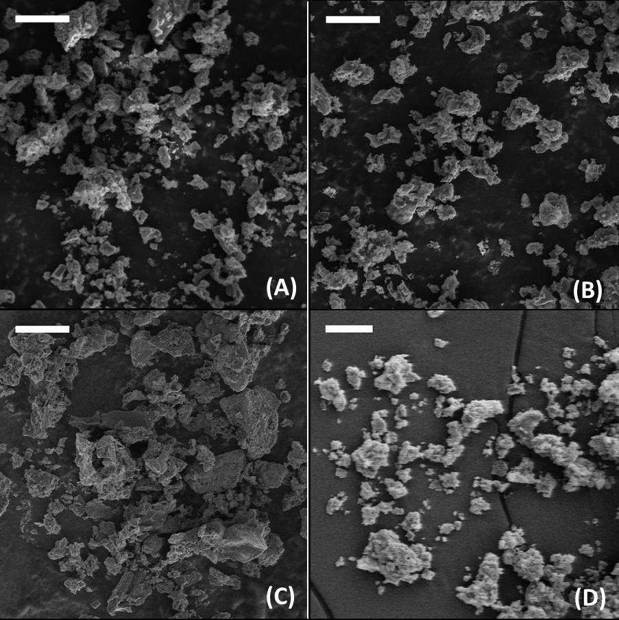
4 Supplementary Figure 3 SEM images and EDS spectra of mpsi materials. SEM images of (A) mpsi-600; (B) mpsi-700; (C) mpsi-820 and (D) mpsi-600r. The scale bars are 20 µm. EDS spectra of (E) mpsi-600; (F) mpsi-700; (G) mpsi-820 and (H) mpsi-600r 4
5 Supplementary Figure 4 XPS fitting. The XPS spectra and their fitting results of (A) mpsi-600, (B) mpsi-700, (C) mpsi-820, (D) mpsi-600r. 5
6 Supplementary Figure 5 Photoluminescence spectra. Photoluminescence spectra of A) mpsi-600, B) mpsi- 600R, C) mpsi-700, and D) mpsi
 of mpsi-600r.")
.")
7 Supplementary Figure 6 Optical spectra. Optical band gap and UV-Vis diffuse reflectance spectra (insert) of mpsi-600r. Supplementary Figure 7 Measured and calculated band gaps. Optical band-gap energies for various Si crystallites with respect to their diameter D (nm). T m and LCAO are corresponding to the theoretical relationship based on size-dependent temperature and linear combination of atomic orbitals technique. 7

8 Supplementary Figure 8 Average H 2 evolution. Average H 2 evolution rate of mpsi and Si nanopowder over 7 hours. Supplementary Figure 9 KOH reaction. Time course of H 2 generation by mpsi-600r chemically reacted with KOH aqueous solution. 8
9 Supplementary Figure 10 Repeatability of photocatalytic tests. (A) Typical reaction time course of the photocatalytic H 2 evolution of different porous Si materials without co-catalyst under 300 W Xenon light; (B) comparison of H 2 evolution activities of mpsi-600r under different light conditions. 9
10 Supplementary Table 1 Oxygen concentration (at %) of all mpsi samples, determined from XPS. Sample O atomic ratio (atom %) mpsi-600r mpsi mpsi mpsi Supplementary Table 2 Primary Particle size, surface area, band gap, and H 2 evolution rate of mpsi materials and Si nano-powder. Primary Particle Size (nm) BET surface area (m 2 g -1 ) Band gap (ev) H 2 evolution rate (μmol h -1 g -1 Si in 7 hours) Si nano-powder mpsi-600 < mpsi-700 ~ mpsi mpsi-600r <
11 Supplementary Discussion Salt distribution in raw products Some salt byproducts were found to precipitate out separately from the Si/salt matrixes, as shown in Supplementary Fig. 1. In a typical synthesis as described in the Method section, 9.95 g of salts were generated according to the stoichiometry of the reaction. The weight of the templating salts is at most 3.04 g (pore volume of 1.44 cm 3 /g for mpsi-600). So, large amount of the salts precipitated out separately. In addition, extra reductant (1.2 fold to stoichiometric amount) was used in the synthesis to push the reaction to completion. After quenching the unreacted NaK by HCl/ether, an extra 1.99 g of salts should stoichiometrically have been generated. These salts also precipitated out separately. Without their growth being restricted by the silicon framework, we would expect these salts to grow larger than those within the framework. This is supported by TEM imaging; a representative image of these large salt particles is shown in Supplementary Fig. 1. It is clear that these external salts have a nonuniform particle size distribution from 10 nm to 50 nm, with individual particles being composed of smaller multi-crystals. The average crystallite size calculated from the XRD result (Fig. 2A) by the Scherrer equation is 22 nm for KCl and 31 nm for NaCl, which is still a reasonable number considering the multi-crystalline nature of those large salt particles. Discussion of photoluminescence (PL) of all mpsi Photoluminescence (PL) spectra of all the samples have been collected and shown in Supplementary Fig. 5. As the PL peak positions are related to the particle size and our particle size distribution is broader than in previous reports on the PL behavior of Si quantum dots, we can observe at least two peaks in the spectra. In comparison to the mpsi-600 and mpsi-600r samples, the PL peak intensity becomes lower and peak position shifts to a longer wavelength in the mpsi-700 and mpsi-820 samples, which matches the expected decrease in quantum confinement with increasing particle size. Both the PL phenomena and the shift of PL peaks prove the shift of band gap due to quantum confinement. 1 Band gap-crystallite size relations As shown in Supplementary Fig. 7, we have compared our experimentally-obtained band gap-crystallite size relationships with theoretical calculations based on a size-dependent temperature(t m ) model and linear combination of atomic orbitals (LCAO) technique. 2, 3 The crystallite sizes chosen for this calculation are based on applying the Scherrer equation to the XRD data for each sample. The band gap of mpsi-600 is in between the band gaps predicted by these two models, while the band gaps of mpsi-700 and mpsi-820 are slightly larger than the predicted values. The band gap from the UV-vis reflection measurements is the overall effect of the whole particle size distribution. As there are also some smaller particles in the mpsi-700 and mpsi-820 samples (as observed by HRTEM), and these smaller particles will contribute more than the larger ones to the observed band gap, 1 it is reasonable that our measured band gaps for these samples are slightly larger than the theoretical results. In addition, the amorphous Si and Si oxides present in the samples may also have some effect on the band gaps, but this effect is expected to be minor due to their low content. 11
12 Fitting of XPS peak components We note that there is disagreement in the literature on the best way to fit SiO x -containing XPS spectra. In addition, as demonstrated in a number of existing papers, it is important to have appropriate reference samples from which to get accurate peak parameters. 4-6 It is unclear what type of reference materials would accurately reflect the XPS peaks of our uniquely-structured mpsi materials, or how to fully account for factors such as variable oxide thickness effects or differential charging in our samples. Due to this lack of reliable reference samples and disagreement among existing publications on the best way to fit such spectra, the XPS peak fittings of our materials can only provide approximate fractions of oxide contents they may not necessarily reflect the real composition distribution. Supplementary References 1. Kux, A., Ben Chorin, M. Band gap of porous silicon. Phys. Rev. B 51, (1995). 2. Li, M., Li, J. C., Jiang, Q. Size-dependent band-gap and dielectric constant of Si nanocrystals. Int. J. Mod Phys B 24, (2010). 3. Delerue, C., Allan, G., Lannoo, M. Theoretical aspects of the luminescence of porous silicon. Phys. Rev. B 48, (1993). 4. Shallenberger, J. R. Determination of chemistry and microstructure in SiO x (0.1<x<0.8) films by x-ray photoelectron spectroscopy. J. Vac. Sci. Technol., A 14, (1996). 5. Alexander, M. R., Short, R. D., Jones, F. R., Michaeli, W., Blomfield, C. J. A study of HMDSO/O 2 plasma deposits using a high-sensitivity and -energy resolution XPS instrument: curve fitting of the Si 2p core level. Appl. Surf. Sci. 137, (1999). 6. Iwata, S., Ishizaka, A. Electron spectroscopic analysis of the SiO 2 /Si system and correlation with metal oxide semiconductor device characteristics. J. Appl. Phys. 79, (1996). 12
Red luminescence from Si quantum dots embedded in SiO x films grown with controlled stoichiometry
 Red luminescence from Si quantum dots embedded in films grown with controlled stoichiometry Zhitao Kang, Brannon Arnold, Christopher Summers, Brent Wagner Georgia Institute of Technology, Atlanta, GA 30332
Supplementary Information
 Supplementary Information Supplementary Figure 1 Characterization of precursor coated on salt template. (a) SEM image of Mo precursor coated on NaCl. Scale bar, 50 μm. (b) EDS of Mo precursor coated on
Supplementary Figure S1 Photograph of MoS 2 and WS 2 flakes exfoliated by different metal naphthalenide (metal = Na, K, Li), and dispersed in water.
, and dispersed in water.") Supplementary Figure S1 Photograph of MoS 2 and WS 2 flakes exfoliated by different metal naphthalenide (metal = Na, K, Li), and dispersed in water. Supplementary Figure S2 AFM measurement of typical LTMDs
Supplementary Figure S1 Photograph of MoS 2 and WS 2 flakes exfoliated by different metal naphthalenide (metal = Na, K, Li), and dispersed in water. Supplementary Figure S2 AFM measurement of typical LTMDs
Structural Characterization of Nano-porous Materials
 Structural Characterization of Nano-porous Materials Techniques for characterization of nano-porous materials Crystalline structure - Single crystal & Powder X-ray diffraction (XRD) - Electron crystallography
Summary Chapter Chapter Chapter
 Ceria (CeO 2 ) has been extensively employed as an important component of automotive three-way catalysts (TWC) for reducing the exhaust pollutants. Besides this, fuel cell processes, oxygen permeation
CHAPTER 8 CONCLUSIONS AND SCOPE FOR FUTURE WORK
 CHAPTER 8 CONCLUSIONS AND SCOPE FOR FUTURE WORK In this thesis an experimental investigation about Magnisium oxide (MgO) nanoparticles and its nanocomposites i.e.mgo-x (X= NiO, CuO, Co3O4, Fe2O3, CeO2,
Experimental Study on Nitrogen-Doped Nano-Scale TiO 2 Prepared by Microwave-Assisted Process at Low Temperature
 Modern Applied Science February, 2010 Experimental Study on Nitrogen-Doped Nano-Scale TiO 2 Prepared by Microwave-Assisted Process at Low Temperature Zengxiu Zhai (Corresponding author) College of Material
Cathodoluminescence measurements of suboxide band-tail and Si dangling bond states at ultrathin Si SiO 2 interfaces
 Cathodoluminescence measurements of suboxide band-tail and Si dangling bond states at ultrathin Si SiO 2 interfaces A. P. Young a) Department of Electrical Engineering, The Ohio State University, Columbus,
High Density Iron Silicide Nanodots Formed by Ultrathin SiO 2 Film Technique
 Available online at www.sciencedirect.com Procedia Engineering 36 (2012 ) 382 387 IUMRS-ICA 2011 High Density Iron Silicide Nanodots Formed by Ultrathin SiO 2 Film Technique Yoshiaki Nakamura a,b* a Graduate
Chapter 5. Influence of Pb 2+ doping on photoluminescence properties CaSiO 3 : Mn 2+ nanophosphor
 142 Chapter 5 Influence of Pb 2+ doping on photoluminescence properties CaSiO 3 : Mn 2+ nanophosphor 143 Chapter-5: Influence of Pb 2+ doping on photoluminescence Properties CaSiO3: Mn 2+ nanophosphor
Supplementary Figure 1. (a-d). SEM images of h-bn film on iron foil with corresponding Raman spectra. Iron foil was reused for re-growth of h-bn
. SEM images of h-bn film on iron foil with corresponding Raman spectra. Iron foil was reused for re-growth of h-bn") Supplementary Figure 1. (a-d). SEM images of h-bn film on iron foil with corresponding Raman spectra. Iron foil was reused for re-growth of h-bn after bubbling transfer. Scale bars (ad) 20 μm. Supplementary
Supplementary Figure 1. (a-d). SEM images of h-bn film on iron foil with corresponding Raman spectra. Iron foil was reused for re-growth of h-bn after bubbling transfer. Scale bars (ad) 20 μm. Supplementary
PREPARATION OF VISIBLE-LIGHT-DRIVEN TIO 2 PHOTOCATALYST DOPED WITH IRON IN SUPERCRITICAL CARBON DIOXIDE
 PREPARATION OF VISIBLE-LIGHT-DRIVEN TIO 2 PHOTOCATALYST DOPED WITH IRON IN SUPERCRITICAL CARBON DIOXIDE Esther Alonso *, Héctor Fernández-Rodríguez and M.J. Cocero Department of Chemical Engineering &
Formation of and Light Emission from Si nanocrystals Embedded in Amorphous Silicon Oxides
 10.1149/1.2392914, copyright The Electrochemical Society Formation of and Light Emission from Si nanocrystals Embedded in Amorphous Silicon Oxides D. Comedi a, O. H. Y. Zalloum b, D. E. Blakie b, J. Wojcik
Pre-treatment of low temperature GaN buffer layer deposited on AlN Si substrate by hydride vapor phase epitaxy
 Ž. Surface and Coatings Technology 131 000 465 469 Pre-treatment of low temperature GaN buffer layer deposited on AlN Si substrate by hydride vapor phase epitaxy Ha Jin Kim, Ho-Sun Paek, Ji-Beom Yoo Department
College of Chemistry and Materials Engineering, Wenzhou University, Wenzhou , China.
 Electronic Supplementary Material (ESI) for ChemComm. This journal is The Royal Society of Chemistry 2017 Supporting Information Use of long-term stable CsPbBr 3 perovskite quantum dots in phospho-silicate
Structure and Luminescence Properties of Y 2 O 3 :Eu 3+ Nanophosphors
 Journal of Atomic, Molecular, Condensate & Nano Physics Vol. 3, No. 1, pp. 55 60, 2016 ISSN 2349-2716 (online); 2349-6088 (print) Published by RGN Publications http://www.rgnpublications.com Structure
Supplementary Figure 1. SEM and TEM images of CoO/CNF before and after galvanostatic cycles. (a) SEM image of CNF. (b) SEM image of CoO NPs uniformly
 SEM image of CNF. (b) SEM image of CoO NPs uniformly") Supplementary Figure 1. SEM and TEM images of CoO/CNF before and after galvanostatic cycles. (a) SEM image of CNF. (b) SEM image of CoO NPs uniformly distributed on CNF. (c) SEM image of 2-cycle CoO/CNF.
Supplementary Figure 1. SEM and TEM images of CoO/CNF before and after galvanostatic cycles. (a) SEM image of CNF. (b) SEM image of CoO NPs uniformly distributed on CNF. (c) SEM image of 2-cycle CoO/CNF.
GROWTH MECHANISM OF NANODIMENSIONAL VANADIUM DIOXIDE ON SILICON SURFACE OBTAINED BY ML-ALD METHOD
 184 Rev. Adv. Mater. Sci. 27 (2011) 184-188 O.M. Osmolowskaya and V.M. Smirnov GROWTH MECHANISM OF NANODIMENSIONAL VANADIUM DIOXIDE ON SILICON SURFACE OBTAINED BY ML-ALD METHOD Saint-Petersburg State University,
Synthesis and Characterization of Cadmium Sulfide Nanoparticles
 Synthesis and Characterization of Cadmium Sulfide Nanoparticles R.Hepzi Pramila Devamani 1*, R.Kiruthika, P.Mahadevi and S.Sagithapriya 2 1 1. Assistant Professor, Department of Physics, V.V.Vanniaperumal
PHOTOLUMINESCENCE STUDIES OF NANO PHOSPHOR Sr 2 CeO 4 :USING COMBUSTION TECHNIQUE
 ISSN 976 1411 Available online at www.internationalejournals.com International ejournals International ejournal of Mathematics and Engineering 132 (211) 124-128 PHOTOLUMINESCENCE STUDIES OF NANO PHOSPHOR
Supporting Information
 Copyright WILEY VCH Verlag GmbH & Co. KGaA, 69469 Weinheim, Germany, 2012. Supporting Information for Small, DOI: 10.1002/smll. 201102654 Large-Area Vapor-Phase Growth and Characterization of MoS 2 Atomic
Romanian Academy Institute of Physical Chemistry Ilie Murgulescu. PhD THESIS SUMMARY
 Romanian Academy Institute of Physical Chemistry Ilie Murgulescu PhD THESIS SUMMARY CORRELATIONS BETWEEN STRUCTURAL AND PHYSICO - CHEMICAL PROPERTIES OF THE SEMICONDUCTOR OXIDES WITH OPTIC, SENSORISTIC
CHAPTER 4. SYNTHESIS OF ALUMINIUM SELENIDE (Al 2 Se 3 ) NANO PARTICLES, DEPOSITION AND CHARACTERIZATION
 NANO PARTICLES, DEPOSITION AND CHARACTERIZATION") 40 CHAPTER 4 SYNTHESIS OF ALUMINIUM SELENIDE (Al 2 Se 3 ) NANO PARTICLES, DEPOSITION AND CHARACTERIZATION 4.1 INTRODUCTION Aluminium selenide is the chemical compound Al 2 Se 3 and has been used as a precursor
40 CHAPTER 4 SYNTHESIS OF ALUMINIUM SELENIDE (Al 2 Se 3 ) NANO PARTICLES, DEPOSITION AND CHARACTERIZATION 4.1 INTRODUCTION Aluminium selenide is the chemical compound Al 2 Se 3 and has been used as a precursor
SYNTHESIS OF Fe NANOPARTICLES BY REDOX REACTION USING AN ELECTRON BEAM DEPOSITION TECHNIQUE
 International Journal of Nanoscience Vol. 3, Nos. 4 & 5 (2004) 631 638 c WorldScientific Publishing Company SYNTHESIS OF Fe NANOPARTICLES BY REDOX REACTION USING AN ELECTRON BEAM DEPOSITION TECHNIQUE S.
Biomimetic synthesis of gold nanocrystals using a reducing amphiphile. Ferdinand Gonzaga, Sherdeep Singh and Michael A. Brook. Department of Chemistry
 Biomimetic synthesis of gold nanocrystals using a reducing amphiphile. Ferdinand Gonzaga, Sherdeep Singh and Michael A. Brook Department of Chemistry 1280 Main St. W. Hamilton ON L8S 4M1 Canada Outline
An Analysis of Structural and Optical Properties Undoped ZnS and Doped (with Mn, Ni) ZnS Nano Particles
 ZnS Nano Particles") Journal of Modern Physics, 213, 4, 122-126 http://dx.doi.org/1.4236/jmp.213.47137 Published Online July 213 (http://www.scirp.org/journal/jmp) An Analysis of Structural and Optical Properties Undoped ZnS
Journal of Modern Physics, 213, 4, 122-126 http://dx.doi.org/1.4236/jmp.213.47137 Published Online July 213 (http://www.scirp.org/journal/jmp) An Analysis of Structural and Optical Properties Undoped ZnS
Interface potential measurement with electron spectroscopic method
 Journal of Surface Analysis Vol.13 No. 2 (2006) pp. 185-189 Interface potential measurement with electron spectroscopic method Michiko Yoshitake * and Weijie Song National Research Institute for Materials
Development of Low-resistivity TiN Films using Cat Radical Sources
 Development of Low-resistivity TiN Films using Cat Radical Sources Masamichi Harada*, Yohei Ogawa*, Satoshi Toyoda* and Harunori Ushikawa** In Cu wiring processes in the 32-nm node generation or later,
Supplimentary Information. Large-Scale Synthesis and Functionalization of Hexagonal Boron Nitride. Nanosheets
 Electronic Supplementary Material (ESI) for Nanoscale. This journal is The Royal Society of Chemistry 2014 Supplimentary Information Large-Scale Synthesis and Functionalization of Hexagonal Boron Nitride
Germanium-Silicon Alloy and Core-Shell Nanocrystals by Gas Phase Synthesis
 Electronic Supplementary Material (ESI) for Nanoscale. This journal is The Royal Society of Chemistry 2015 Electronic Supplementary Information for: Germanium-Silicon Alloy and Core-Shell Nanocrystals
A silicon nanocrystals/polymer nanocomposite as down-conversion layer in organic and hybrid solar cells
 Electronic Supplementary Material (ESI) for Nanoscale. This journal is The Royal Society of Chemistry 2015 Supporting Material for A silicon nanocrystals/polymer nanocomposite as down-conversion layer
Supplementary Materials for
 advances.sciencemag.org/cgi/content/full/3/5/e1603171/dc1 Supplementary Materials for Carbon dots in zeolites: A new class of thermally activated delayed fluorescence materials with ultralong lifetimes
Supplementary Electronic Information for:
 Electronic Supplementary Material (ESI) for RSC Advances. This journal is The Royal Society of Chemistry 25 Supplementary Electronic Information for: Nanotoxicity of polyelectrolyte-functionalized titania
Simple fabrication of highly ordered AAO nanotubes
 Journal of Optoelectronic and Biomedical Materials Volume 1, Issue 1, March 2009, p. 79-84 Simple fabrication of highly ordered AAO nanotubes N. Taşaltin a, S. Öztürk a, H. Yüzer b, Z. Z. Öztürk a,b* a
ph-dependent Growth of Atomic Pd Layers on Trisoctahedral Gold Nanoparticles to Realize Enhanced Performance in Electrocatalysis and
 Electronic Supplementary Material (ESI) for Nanoscale. This journal is The Royal Society of Chemistry 2018 ph-dependent Growth of Atomic Pd Layers on Trisoctahedral Gold Nanoparticles to Realize Enhanced
Supporting Information. Solution-Processed 2D PbS Nanoplates with Residual Cu 2 S. Exhibiting Low Resistivity and High Infrared Responsivity
 Supporting Information Solution-Processed 2D PbS Nanoplates with Residual Cu 2 S Exhibiting Low Resistivity and High Infrared Responsivity Wen-Ya Wu, Sabyasachi Chakrabortty, Asim Guchhait, Gloria Yan
It is instructive however for you to do a simple structure by hand. Rocksalt Structure. Quite common in nature. KCl, NaCl, MgO
 Today the structure determinations etc are all computer -assisted It is instructive however for you to do a simple structure by hand Rocksalt Structure Quite common in nature KCl, NaCl, MgO 9-1 Typical
2-1 Introduction The demand for high-density, low-cost, low-power consumption,
 Chapter 2 Hafnium Silicate (HfSi x O y ) Nanocrystal SONOS-Type Flash Memory Fabricated by Sol-Gel Spin Coating Method Using HfCl 4 and SiCl 4 as Precursors 2-1 Introduction The demand for high-density,
Ambient Temperature Aqueous Synthesis of Ultrasmall Copper Doped Ceria. Nanocrystals for the Water Gas Shift and Carbon Monoxide Oxidation Reactions
 Electronic Supplementary Material (ESI) for Journal of Materials Chemistry A. This journal is The Royal Society of Chemistry 2017 Ambient Temperature Aqueous Synthesis of Ultrasmall Copper Doped Ceria
SUPPLEMENTARY INFORMATION
 An electrodeposited inhomogeneous metal insulator semiconductor junction for efficient photoelectrochemical water oxidation James C. Hill, Alan T. Landers, Jay A. Switzer * Missouri University of Science
OPTICAL PROPERTIES OF NANO-CRYSTALLINE SILICON FILMS PREPARED BY USING SOL-GEL SPIN COATING PROCESS
 OPTICAL PROPERTIES OF NANO-CRYSTALLINE SILICON FILMS PREPARED BY USING SOL-GEL SPIN COATING PROCESS T. Fangsuwannarak,* and K. Khunchana School of Electrical Engineering Suranaree University of Technology
How can we describe a crystal?
 How can we describe a crystal? Examples of common structures: (1) The Sodium Chloride (NaCl) Structure (LiH, MgO, MnO, AgBr, PbS, KCl, KBr) The NaCl structure is FCC The basis consists of one Na atom and
Luminescence properties of ultrasmall amorphous Si nanoparticles with sizes smaller than 2 nm
 Journal of Crystal Growth 304 (2007) 476 480 www.elsevier.com/locate/jcrysgro Luminescence properties of ultrasmall amorphous Si nanoparticles with sizes smaller than 2 nm Y. Xie a, X.L. Wu a,b,, T. Qiu
Structural, optical properties of crystalline silicon (c-si) deposited. on porous aluminium by PECVD technique
 deposited. on porous aluminium by PECVD technique") Structural, optical properties of crystalline silicon (c-si) deposited on porous aluminium by PECVD technique M. Ghrib 1, T. Abdellaoui 1, N. Khedher 1, M. Gaidi 1, M. Ben Salem 2, Hatem Ezzaouia 1, 1
Structural, optical properties of crystalline silicon (c-si) deposited on porous aluminium by PECVD technique M. Ghrib 1, T. Abdellaoui 1, N. Khedher 1, M. Gaidi 1, M. Ben Salem 2, Hatem Ezzaouia 1, 1
ATOMIC LAYER DEPOSITION FOR PHOTONIC CRYSTAL DEVICES
 ATOMIC LAYER DEPOSITION FOR PHOTONIC CRYSTAL DEVICES E. Graugnard, J. S. King, D. Heineman, and C. J. Summers School of Materials Science and Engineering, Georgia Institute of Technology, Atlanta, GA,
Supplementary Information
 Supplementary Information Direct manufacturing of ultrathin graphite on three- dimensional nanoscale features Mercè Pacios, Peiman Hosseini, Ye Fan, Zhengyu He, Oliver Krause, John Hutchison, Jamie H.
Supplementary Information
 Supplementary Information Oxygen-Deficient Zirconia (ZrO2-x): A New Material for Solar Light Absorption Apurba Sinhamahapatra 1, Jong-Pil Jeon 1, Joonhee Kang 1, Byungchan Han 2, * and Jong-Sung Yu 1,
Supplementary Figure S1. High-resolution XPS spectra in the Cu 2p region and Cu LMM spectra are shown in (A) and (B) respectively for CdSe NCs
 and (B) respectively for CdSe NCs") Supplementary Figure S1. High-resolution XPS spectra in the Cu 2p region and Cu LMM spectra are shown in (A) and (B) respectively for CdSe NCs treated with 651 Cu + ions per NC and in (C) and (D) respectively
Supplementary Figure S1. High-resolution XPS spectra in the Cu 2p region and Cu LMM spectra are shown in (A) and (B) respectively for CdSe NCs treated with 651 Cu + ions per NC and in (C) and (D) respectively
CHAPTER 4 SYNTHESIS, CHARACTERIZATION AND MICROENCAPSULATION PROCESS OF THE NANO SILICA
 70 CHAPTER 4 SYNTHESIS, CHARACTERIZATION AND MICROENCAPSULATION PROCESS OF THE NANO SILICA 4.1 INTRODUCTION This chapter is concerned with the synthesis of nano silica particles from the natural resources
Chapter 3. Deposition and Characterization of yttrium oxide (Y 2 O 3 ) thin films
 thin films") Chapter 3 Deposition and Characterization of yttrium oxide (Y 2 O 3 ) thin films This chapter describes about the deposition of yttrium oxide thin films by RF plasma enhanced MOCVD technique using Y(thd)
Chapter 3 Deposition and Characterization of yttrium oxide (Y 2 O 3 ) thin films This chapter describes about the deposition of yttrium oxide thin films by RF plasma enhanced MOCVD technique using Y(thd)
Supporting Information. Trapping the Catalyst Working State by Amber-Inspired Hybrid
 Supporting Information Trapping the Catalyst Working State by Amber-Inspired Hybrid Material and Revealing the Cobalt Nanostructure Evolution in Gas-to- Liquid Processing Bingbing Zhang a, Haiquan Su a*,
Microstructure, morphology and their annealing behaviors of alumina films synthesized by ion beam assisted deposition
 Nuclear Instruments and Methods in Physics Research B 206 (2003) 357 361 www.elsevier.com/locate/nimb Microstructure, morphology and their annealing behaviors of alumina films synthesized by ion beam assisted
Polycrystalline and microcrystalline silicon
 6 Polycrystalline and microcrystalline silicon In this chapter, the material properties of hot-wire deposited microcrystalline silicon are presented. Compared to polycrystalline silicon, microcrystalline
Linlin Xin a and Xuefeng Liu b. School of Chemical and Material Engineering, Jiangnan University, Wuxi, , PR China.
 Electronic Supplementary Material (ESI) for RSC Advances. This journal is The Royal Society of Chemistry 215 Electronic Supplementary Information Black TiO 2 Inverse Opals for Visible-Light Photocatalysis
Supporting Information:
 Supporting Information: Radial-Position-Controlled Doping in CdS/ZnS Core/Shell Nanocrystals Yongan Yang, Ou Chen, Alexander Angerhofer and Y. Charles Cao* Department of Chemistry, University of Florida,
Investigation of Au-Hg Amalgam Formation on. Substrate-Immobilized Individual Au Nanorods
 Electronic Supplementary Material (ESI) for Journal of Materials Chemistry C. This journal is The Royal Society of Chemistry 2015 Supporting Information Investigation of Au-Hg Amalgam Formation on Substrate-Immobilized
Optical, microstructural and electrical studies on sol gel derived TiO 2 thin films
 Indian Journal of Pure & Applied Physics Vol. 55, January 2017, pp. 81-85 Optical, microstructural and electrical studies on sol gel derived TiO 2 thin films M Bilal Tahir*, S Hajra, M Rizwan & M Rafique
Supplementary Information
 Supplementary Information Formation of oxygen vacancies and Ti 3+ state in TiO 2 thin film and enhanced optical properties by air plasma treatment Bandna Bharti a, Santosh Kumar b, Heung-No Lee c and Rajesh
Characteristics of Hafnium-Aluminum-Oxide Thin Films Deposited by Using Atomic Layer Deposition with Various Aluminum Compositions
 Journal of the Korean Physical Society, Vol. 47, No. 3, September 2005, pp. 501 507 Characteristics of Hafnium-Aluminum-Oxide Thin Films Deposited by Using Atomic Layer Deposition with Various Aluminum
XPS STUDY OF DIAMOND-LIKE CARBON-BASED NANOCOMPOSITE FILMS
 International Journal of Nanoscience Vol. 3, No. 6 (2004) 797 802 c World Scientific Publishing Company XPS STUDY OF DIAMOND-LIKE CARBON-BASED NANOCOMPOSITE FILMS S. ZHANG,Y.Q.FU,X.L.BUIandH.J.DU School
لبا ب ةعماج / ةيساسلأا ةيبرتلا ةيلك ة لجم
 Photoluminescence from Etched Silicon Surface by High Power Laser Oday A. Abbass Department of Physics/College of Sciences/University of Kufa ABSTRACT Porous silicon layers (P-Si) has been prepared in
Solid-Phase Synthesis of Mg2Si Thin Film on Sapphire substrate
 Proc. Asia-Pacific Conf. on Semiconducting Silicides and Related Materials 2016 JJAP Conf. Proc. 5, https://doi.org/10.7567/jjapcp.5.011302 Solid-Phase Synthesis of Mg2Si Thin Film on Sapphire substrate
SYNTHESIS OF SI NANOPARTICLES FROM FREESTANDING POROUS SILICON (PS) FILM USING ULTRASONICATION
 FILM USING ULTRASONICATION") SYNTHESIS OF SI NANOPARTICLES FROM FREESTANDING POROUS SILICON (PS) FILM USING ULTRASONICATION Paresh G. Kale and Chetan S. Solanki Indian Institute of Technology Bombay, Mumbai, Maharashtra, India ABSTRACT
SYNTHESIS OF SI NANOPARTICLES FROM FREESTANDING POROUS SILICON (PS) FILM USING ULTRASONICATION Paresh G. Kale and Chetan S. Solanki Indian Institute of Technology Bombay, Mumbai, Maharashtra, India ABSTRACT
Passivation of InAs and GaSb with novel high dielectrics
 Passivation of InAs and GaSb with novel high dielectrics Professor Minghwei HONG Department of Materials Science and Engineering, National Tsing Hua University 101, Section 2, Kuang-Fu Rd., Hsinchu, Taiwan,
Structural and Optical properties of Nickel Sulphide(NiS) nanoparticles
 nanoparticles") International Journal of NanoScience and Nanotechnology. ISSN 0974-3081 Volume 6, Number 1 (2015), pp. 41-45 International Research Publication House http://www.irphouse.com Structural and Optical properties
International Journal of NanoScience and Nanotechnology. ISSN 0974-3081 Volume 6, Number 1 (2015), pp. 41-45 International Research Publication House http://www.irphouse.com Structural and Optical properties
Deposited by Sputtering of Sn and SnO 2
 Journal of the Korean Ceramic Society Vol. 49, No. 5, pp. 448~453, 2012. http://dx.doi.org/10.4191/kcers.2012.49.5.448 Comparative Study of Nitrogen Incorporated SnO 2 Deposited by Sputtering of Sn and
X-Ray Reflectivity Study of Hafnium Silicate Thin Films Prepared by Thermal Chemical Vapor Deposition
 X-Ray Reflectivity Study of Hafnium Silicate Thin Films Prepared by Thermal Chemical Vapor Deposition Hideyuki YAMAZAKI, Advanced LSI Technology Laboratory, Toshiba Corporation hideyuki.yamazaki@toshiba.co.jp
Ion Irradiation Enhanced Formation and Luminescence of Silicon Nanoclusters from a-sio x
 Journal of the Korean Physical Society, Vol. 39, December 2001, pp. S83 S87 Ion Irradiation Enhanced Formation and Luminescence of Silicon Nanoclusters from a-sio x Yohan Sun, Se-Young Seo and Jung H.
Supporting Online Material for
 www.sciencemag.org/cgi/content/full/science.1200448/dc1 Supporting Online Material for Increasing Solar Absorption for Photocatalysis with Black Hydrogenated Titanium Dioxide Nanocrystals This PDF file
Size Dependent Anisotropic Strain and Optical Properties of Strained Si Nanocrystals
 Copyright 2011 American Scientific Publishers All rights reserved Printed in the United States of America Journal of Nanoscience and Nanotechnology Vol. 11, 1 7, 2011 Size Dependent Anisotropic Strain
Amorphous Er 2 O 3 films for antireflection coatings
 Amorphous Er 2 O 3 films for antireflection coatings Zhu Yan-Yan( 朱燕艳 ) a), Fang Ze-Bo( 方泽波 ) b), and Liu Yong-Sheng( 刘永生 ) a) a) Shanghai University of Electric Power, Shanghai 200090, China b) Department
CHAPTER 6 STRUCTURAL AND OPTICAL PROPERTIES OF. CdSe/CdTe MULTILAYER THIN FILMS
 CHAPTER 6 STRUCTURAL AND OPTICAL PROPERTIES OF CdSe/CdTe MULTILAYER THIN FILMS CHAPTER 6 STRUCTURAL AND OPTICAL PROPERTIES OF CdSe/CdTe MULTILAYER THIN FILMS 6.1 INTRODUCTION Quantum size effects in semiconductors
Structure and optical properties of M/ZnO (M=Au, Cu, Pt) nanocomposites
 nanocomposites") Solar Energy Materials & Solar Cells 8 () 339 38 Structure and optical properties of M/ (M=Au, Cu, Pt) nanocomposites U. Pal a,b, *, J. Garc!ıa-Serrano a, G. Casarrubias-Segura a, N. Koshizaki c, T. Sasaki
Solar Energy Materials & Solar Cells 8 () 339 38 Structure and optical properties of M/ (M=Au, Cu, Pt) nanocomposites U. Pal a,b, *, J. Garc!ıa-Serrano a, G. Casarrubias-Segura a, N. Koshizaki c, T. Sasaki
Tunable Photocatalytic Selectivity of Hollow TiO 2 Microspheres Composed of Anatase Polyhedra with Exposed {001} Facets
 Tunable Photocatalytic Selectivity of Hollow TiO 2 Microspheres Composed of Anatase Polyhedra with Exposed {001} Facets Shengwei Liu, a Jiaguo Yu, a,* and Mietek Jaroniec b,* a State Key Laboratory of
Passivation of Porous Silicon by LaF 3 Using a Simple Single-Source Chemical Bath Technique
 International Journal of Materials and Chemistry 2012, 2(3): 111-115 DOI: 10.5923/j.ijmc.20120203.05 Passivation of Porous Silicon by LaF 3 Using a Simple Abdul Al Mortuza 1, Md. Hafizur Rahman 2, Sinthia
Optical parameter determination of ZrO 2 thin films prepared by sol gel dip coating
 International Journal of ChemTech Research CODEN (USA): IJCRGG ISSN : 0974-490 Vol.6, No.13, pp 534-5346, November 014 MESCon 014 [4th -5 th September 014] National Conference on Material for Energy Storage
Chapter 3. In this chapter, we use sol-gel method to combine three high-k precursors, i.e. HfCl 4, ZrCl 4 and SiCl 4 together to form hafnium silicate
 Chapter 3 Sol-Gel-Derived Zirconium Silicate (ZrSi x O y ) and Hafnium Silicate (HfSi x O y ) Co-existed Nanocrystal SONOS Memory 3-1 Introduction In the previous chapter, we fabricate the sol-gel-derived
Supplementary Information. Solution-phase Synthesis of Cesium Lead Halide Perovskite Nanowires
 Supplementary Information Solution-phase Synthesis of Cesium Lead Halide Perovskite Nanowires Dandan Zhang,,, Samuel W. Eaton,, Yi Yu, Letian Dou,, Peidong Yang*,,,, Department of Chemistry, Department
De-ionized water. Nickel target. Supplementary Figure S1. A schematic illustration of the experimental setup.
 Graphite Electrode Graphite Electrode De-ionized water Nickel target Supplementary Figure S1. A schematic illustration of the experimental setup. Intensity ( a.u.) Ni(OH) 2 deposited on the graphite blank
State Key Laboratory of Advanced Electromagnetic Engineering and Technology, School of
 Electronic Supplementary Material (ESI) for Nanoscale. This journal is The Royal Society of Chemistry 2018 Electrocatalysis of polysulfide conversion by conductive RuO 2 Nano Dots for lithium sulfur batteries
Hei Wong.
 Defects and Disorders in Hafnium Oxide and at Hafnium Oxide/Silicon Interface Hei Wong City University of Hong Kong Email: heiwong@ieee.org Tokyo MQ2012 1 Outline 1. Introduction, disorders and defects
Supplementary Figures
 1635 Reflectance / a.u. 3425 Supplementary Figures T-3 T-2 T-1 4000 3500 3000 2500 2000 1500 1000 Wavenumber / cm -1 Supplementary Figure 1 FTIR spectra of rutile TiO2 samples. Two bands at 1635 and 3425
MASTER'S THESIS. Synthesis of rare-earth oxide mesoporous structures by combustion synthesis
 MASTER'S THESIS 2009:114 Synthesis of rare-earth oxide mesoporous structures by combustion synthesis Etienne Letournel Luleå University of Technology Master Thesis, Continuation Courses Chemical and Biochemical
Bright luminescence from erbium doped nc-si=sio 2 superlattices
 Journal of Non-Crystalline Solids 299 302 (2002) 678 682 www.elsevier.com/locate/jnoncrysol Bright luminescence from erbium doped nc-si=sio 2 superlattices M. Schmidt a, *, J. Heitmann b, R. Scholz b,
Chemically Tunable Full Spectrum Optical Properties of 2D Silicon Telluride Nanoplates
 SUPPORTING INFORMATION Chemically Tunable Full Spectrum Optical Properties of 2D Silicon Telluride Nanoplates Mengjing Wang,, Gabriella Lahti, David Williams, and Kristie J. Koski * Department of Chemistry,
Effect of Incorporated Nitrogen on the Band Alignment of Ultrathin Silicon-oxynitride Films as a Function of the Plasma Nitridation Conditions
 Journal of the Korean Physical Society, Vol. 58, No. 5, May 2011, pp. 1169 1173 Effect of Incorporated Nitrogen on the Band Alignment of Ultrathin Silicon-oxynitride Films as a Function of the Plasma Nitridation
Tungsten Oxide Nanorods Array and Nanobundle Prepared by Using Chemical Vapor Deposition Technique
 Nanoscale Res Lett (7) :45 49 DOI 1.17/s11671-7-975-3 NANO EXPRESS Tungsten Oxide Nanorods Array and Nanobundle Prepared by Using Chemical Vapor Deposition Technique X. P. Wang Æ B. Q. Yang Æ H. X. Zhang
Impurity free vacancy disordering of InGaAs quantum dots
 JOURNAL OF APPLIED PHYSICS VOLUME 96, NUMBER 12 15 DECEMBER 2004 Impurity free vacancy disordering of InGaAs quantum dots P. Lever, H. H. Tan, and C. Jagadish Department of Electronic Materials Engineering,
Rare Earth Doping of Silicon-Rich Silicon Oxide for Silicon-Based Optoelectronic Applications
 Journal of the Korean Physical Society, Vol. 39, December 2001, pp. S78 S82 Rare Earth Doping of Silicon-Rich Silicon Oxide for Silicon-Based Optoelectronic Applications Se-Young Seo, Hak-Seung Han and
1. Aluminum alloys for direct contacts. 1.1 Advantages of aluminum alloys for direct contacts
 Direct contacts between aluminum alloys and thin film transistors (TFTs) contact layers were studied. An Al-Ni alloy was found to be contacted directly with an indium tin oxide (ITO) layer successfully
Synthesis of Red-emitting Nanocrystalline Phosphor CaAlSiN 3 :Eu. Derived from Element Constituents
 Electronic Supplementary Material (ESI) for RSC Advances. This journal is The Royal Society of Chemistry 2014 Electronic Supplementary information Synthesis of Red-emitting Nanocrystalline Phosphor CaAlSiN
Characterization of SrAlO:Dy nano phosphors
 International Journal of Materials Physics. ISSN 0974-309X Volume 7, Number 1 (2016), pp. 9-13 International Research Publication House http://www.irphouse.com Characterization of SrAlO:Dy nano phosphors
Investigation of molybdenum-carbon films Mo C:H deposited using an electron cyclotron resonance chemical vapor deposition system
 JOURNAL OF APPLIED PHYSICS VOLUME 88, NUMBER 6 15 SEPTEMBER 2000 Investigation of molybdenum-carbon films Mo C:H deposited using an electron cyclotron resonance chemical vapor deposition system Rusli,
Europium-Doped ZnAl2O4 Nanophosphors: Structural and Luminescence Properties
 Proceedings of the World Congress on New Technologies (NewTech 2015) Barcelona, Spain July 15-17, 2015 Paper No. 360 Europium-Doped ZnAl2O4 Nanophosphors: Structural and Luminescence Properties A. Fernández-Osorio,
Supporting Information. Bright YAG:Ce nanorod phosphors prepared via a partial wet. chemical route and biolabeling applications
 Supporting Information Bright YAG:Ce nanorod phosphors prepared via a partial wet chemical route and biolabeling applications Daidong Guo, a Baojin Ma, a Lili Zhao, a Jichuan Qiu, a Wei Liu, a Yuanhua
Review Article Photoluminescence of Silicon Nanocrystals in Silicon Oxide
 Nanomaterials Volume 27, Article ID 4349, 5 pages doi:.55/27/4349 Review Article Photoluminescence of Silicon Nanocrystals in Silicon Oxide L. Ferraioli, M. Wang, 2, 3 G. Pucker, 2 D. Navarro-Urrios, N.
Chapter 3. Synthesis and characterization. of GDC electrolyte material
 Chapter 3 Synthesis and characterization of GDC electrolyte material 3.1 Introduction Ceria based oxide materials are used as electrolytes for intermediate temperature solid oxide fuel cell (IT-SOFC) applications.
Hydrogen Doped Metal Oxide Semiconductors with Exceptional and Tunable Localized Surface Plasmon Resonances
 Supporting Information for Hydrogen Doped Metal Oxide Semiconductors with Exceptional and Tunable Localized Surface Plasmon Resonances Hefeng Cheng,, Meicheng Wen,, Xiangchao Ma, Yasutaka Kuwahara,, Kohsuke
Synthesis and Characterization of DC Magnetron Sputtered ZnO Thin Films Under High Working Pressures
 Accepted Manuscript Synthesis and Characterization of DC Magnetron Sputtered ZnO Thin Films Under High Working Pressures M. Hezam, N. Tabet, A. Mekki PII: S0040-6090(10)00417-7 DOI: doi: 10.1016/j.tsf.2010.03.091
Supplementary Figure S1. CV curves of gold wire and seamless solid/nanoporous Au electrodes in 0.5 M H 2 SO 4 solution at a scan rate of 100 mv S -1.
 Supplementary Figure S1. CV curves of gold wire and seamless solid/nanoporous Au electrodes in 0.5 M H 2 SO 4 solution at a scan rate of 100 mv S -1. The seamless solid/nanoporous Au electrode was obtained