Laser Micromilling :
|
|
|
- Kevin Greer
- 5 years ago
- Views:
Transcription
1 Laser Micromilling : An Enabling Technology for MicroComponent Replication Martyn Knowles Oxford Lasers Ltd. Unit 8, Moorbrook Park Didcot, Oxon OX11 7HP Tel:
2 Outline Introduction Process Technologies Laser Micro-milling Summary
3 Micro-manufacturing Enabling Bridging the gap between Nano and Macro Disruptive Change our thinking as to How, When & Where products will be manufactured and used Strategic Economic, Reduced Space and Energy Costs, Portability, Productivity

4 The Main Challenges in Micro-Manufacture Feature sizes below 20 µm Tolerances in the range of 1 to 10% of the nominal dimensions (precision engineering <0.01%) Nanotechnology Surface roughness required in the range of 10 to 50 nm that is smaller than the grain size of the material
5 Relevant Toolmaking Expertise Mechanical Processes Micro-Milling Micro-Turning Feature Sizes [µm][ Micro-EDM Laser Ablation Energy Assisted Processes Ion Beam Machining
6 Lasers in Micro-manufacturing Established Applications Via drilling Hard disk texturing Lithography etc Factors Enabling Growth Small features Wide variety of materials Flexible Factors Limiting Growth Too slow for mass production (in many but not all cases)
7 Serial Production / Parallel Processing / Replication Most laser processes employ serial production or parallel processing Process speed limited by laser or mechanics/handling Laser + Replication Process Laser - laser milling to create tool/mold - process speed unimportant Replication Process - high speed, mass production Enabling Technology New Laser Applications
 Focussed Ion Beam milling (accurate but v.")
")

8 Why Laser Micro-milling? Other micromilling methods: MicroEDM (material dependent) Focussed Ion Beam milling (accurate but v. slow) Lithography (slow, expensive) Example: 316 s.steel, 1064nm Laser Micromilling 2.5D or 3D milling by laser ablation Most materials can be machined High resolution (very small spot sizes) Flexible setup, Easily interfaced with other processes Easily automated with CAD/CAM software Lady s head 16 x 10 x 2.5mm Main Issues: Laser choice: laser-material interaction expertise necessary. Deleterious thermal effects (melt recast, debris deposit) Post processing sometimes necessary (extra manufacturing step)
9 Micro-scale machining comparison Technology/Feature & geometry Min. feature size/ feature tolerance Feature positional tolerance Material removal rate Materials Focused Ion Beam (FIB) / 2D & 3D 200 nm/20 nm 100 nm 20-30!m 3 /sec Any Micro-milling or - turning/2d or 3D 25!m/2!m 3!m 10,400!m 3 /sec PMMA, aluminium, brass, mild steel Excimer laser/2d or 3D 5!m/ submicron submicron 40,000!m 3 /sec Polymer, ceramics (& metals) fs laser/2d or 3D 2-4!m/ submicron submicron 13,000!m 3 /sec Any Micro-EDM/2D or 3D 25!m / 3!m 3!m 25 millions!m 3 /sec Conductive materials ps laser/2d or 3D 5!m / submicron submicron >100,000!m 3 /sec Any PROFIB/2D & 3D 100 nm/10 nm 100 nm N.B. LIGA can also be used to fabricate parts in polymers, pressed powders, ceramics etc. 1,000!m 3 / sec Any
10 Short-Pulse Laser Ablation Laser Ablation - material removal by a combination of evaporation and melt expulsion. Laser Irradiation Proportion of evaporation vs melt Light Absorption 100% 80% Vaporisation 60% 40% Ablation Material Removal Ejected material (vapour & melt) Recast (melt) material 20% 0% ns 1ns 100ps 1ps Melt Vapour At 1J/cm 2 courtesy Dausinger et al.
11 Processing with Ultrashort Pulses The penetration to which a laser pulse interacts with material is determined by optical and thermal penetration L = L op + L th In dielectrics optical penetration dominates over thermal and for long pulses strongly depends on wavelength. In metals, optical penetration is very short (typically tenth of wavelength) and thermal penetration dominates (function of thermal diffusivity and pulse duration t). L th = 2!(K.t) for t >10ps
12 Processing with Ultrashort Pulses Metals Laser energy is initially absorbed in electrons Electrons thermalize in about 100fs Thermal equilibrium between the electrons and lattice occurs after a multiple of the electron-phonon relaxation time. Typical electron-phonon relaxation are ps. Simple conclusion from this is that for laser pulses less than the electron-phonon relaxation time then no heat transferred to lattice, therefore no melt, thermal damage etc. However, this in not observed in practice and a less simple model explains why.
13 Processing with Ultrashort Pulses Metals As the lattice heats up evaporation starts and continues for several ns. Material stays molten for tens of ns So even for ultrashort pulses, the resulting thermal processes are still in the ns regime and are almost independent of pulse duration for pulse durations <10ps Hence the melt layer is never zero but does approach a minimum which is submicron. There are some effects which depend on pulse duration <10ps and also on pulse frequency and fluence.
14 Processing with Ultrashort Pulses Dielectrics Optical penetration dominates over thermal penetration. High intensity rips electrons out of the lattice. Resulting ions repel each other and cause a Coulomb explosion. Coulomb explosion is a non-thermal ablation mechanism. Tests have shown that in dielectrics material is partly removed by Coulomb explosion and partly thermally. In metals there is no evidence for Coulomb explosion. Ultra-high intensity is desirable to enhance the Coulomb explosion in dielectrics crystals or glass so fs is preferable to ps for processing crystals and glass.
15 Summary of Ultrafast Laser Ablation Metals - Can be processed with fs and ps sources - No advantage for fs, certain disadvantages for fs - 10ps is optimum pulse duration for processing metals. - Lower fluence improves quality - Higher pulse frequency improves speed and there is no quality degradation when the fluences are low and/or velocity high. - Material removal rate for ps laser is > order of magnitude higher than fs because of intensity and pulse frequency considerations. Dielectrics - plastics, polymers (inc. teflon) - High quality results can be achieved with ps and fs sources. - Shorter wavelengths (eg 355nm) enhance results. ns laser pulses can also be used but greater wavelength dependence and increased thermal input Dielectrics - crystals and glass - Can be processed with with ps and fs sources. - Shorter wavelengths (eg 355nm) for the ps source will enhance results. - Best results probably achieved with fs source
16 Lasers Used in this Study c Nd:YAG a MP250 a DP b ML Nd:YVO b 4 ML Nd:YVO 4 Wavelength(nm) Av. Power (W) Pulse Freq. (khz) Max Energy (mj) Pulse Duration 10µs 17ns 30ns 15ps 12ps a Oxford Lasers Ltd b Lumera Laser GmbH c DMG

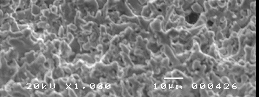


17 Micro-milling Metals : Stainless Steel 1064nm, 10 µs 511nm, 17ns 1064nm, 10ps 20µm 20µm 20µm Thick recast Rough Many voids Ra= µm Thin recast Cracking of recast layer Ra= µm Recast too thin to measure Ra = µm


18 Nanosecond Pulse Ablation : Micro-Milling Examples of optimized processes with nanosecond laser sources Alumina 511nm Tungsten 511nm Diamond 511nm Polyimide 355nm


![Diameter [_m] 50 49 48 47](/docs-images/85/92719677/images/19-7.jpg "46 45 44 1 51 101 151 201")

19 Nanosecond Laser Drilling : Special Case of Micro-milling Si 3 N 4 500µm thick, 511nm Alumina 650µm thick Hole Size Repeatability entrance Exit Diameter [_m] Hole Number exit 90µmØ 50µm Ø, 60µm pitch 50µm square holes


![removal rate: 10 5 µm 3 /s Surface Roughness, Ra [_m] 1.7 1.6 1.5 1.4 1.3 1.](/docs-images/85/92719677/images/20-6.jpg "2 1.1 1 0.1 1 10 100 Volume Removal Rate [x10 7 _m 3 /sec] www.oxfordlasers.")
20 Ceramics ps Nd:Vanadate Laser Alumina (Al 2 O 3 ) 1064nm 100µm 50µm 10µm 1mm 2 square milled with 6 µm raster steps Scan speed: 300 mm/s 50 khz, spot size 17µm Floor surface roughness R a ~0.90 µm Unirradiated surface roughness Ra~0.73 µm Surface roughness increases with raster step size Typical excimer laser removal rate: 10 5 µm 3 /s Surface Roughness, Ra [_m] Volume Removal Rate [x10 7 _m 3 /sec]


21 Dielectrics ps Nd:Vanadate Laser Fused silica nm 500µm 100µm 100µm 1mm 2 square milled out with 2 µm raster steps Floor surface roughness Ra~0.99 µm 0.5W, 50 khz Scan speed mm/s Milled depth µm Some edge chipping present No evidence for laser induced microcracking


![Roughness, Ra [_m] 2](/docs-images/85/92719677/images/22-6.jpg "µm raster steps Floor")


22 Dielectrics ps Nd:Vanadate Laser Fused silica nm 5 µm Surface Roughness, Ra [_m] 2 µm raster steps Floor surf.roughness Ra~0.434 µm Laser Milled Depth [_m]

23 Workstation
24 General Manufacturing workflow 3D CAD modelling: Tool Design CAD model Structuring of tool topography by FIB, Laser ablation, mechanical and chemical processes in polymers soft tooling (pattering of small patchs of the tool surface including critical features) in metal, quartz or ceramics hard tooling moulds/inserts for µim stamps for HE templates for NIL Quality control (SEM, WLI, etc) Replication of polymer, ceramic or glass components
25 Possible Process Chains involving FIB, Laser ablation, NIL and electroforming 3D CAD modelling: design of quartz template Nano- and micro- structuring of quartz templates for the S-FIL process FIB, Laser ablation Micro or nano- pattering of large areas (up to 4 ) in polymers NIL via S-FIL process Transfer the polymer topography in Ni Ni plating and eletroforming Ni inserts and tool integration Serial production of Ni components Serial production of polymer components Hot embossing, µinjection Molding
26 Summary Micro-machining (laser & non-laser) processes have not yet reached the level of precision (%) achieved in macromachining Laser micro-machining can be an enabling technology but is limited in many cases by throughput. Combining laser with other processes e.g. replication, can overcome the throughput problem. Ultrafast lasers are an enabling technology for laser micromilling, especially difficult materials. Picosecond lasers are a good choice for combination of range of materials, machining quality and etch rate.