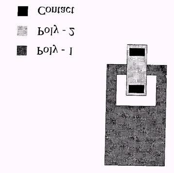
Process Integration. MEMS Release Techniques Sacrificial Layer Removal Substrate Undercut
|
|
|
- Patricia Rogers
- 5 years ago
- Views:
Transcription
1 Process Integration Self-aligned Techniques LOCOS- self-aligned channel stop Self-aligned Source/Drain Lightly Doped Drain (LDD) Self-aligned silicide (SALICIDE) Self-aligned oxide gap MEMS Release Techniques Sacrificial Layer Removal Substrate Undercut Example IC Process Flows NMOS - Generic NMOS Process Flow CMOS - The MOSIS Process Flow Advance MOS Techniques Twin Well CMOS, Retrograde Wells, SOI CMOS 1
2 Self-aligned channel stop with Local Oxidation (LOCOS) LOCOS Process Flow Si 3 N 4 CVD pad oxide Si 2
3 Si B + channel stop dose implant ~10 13 /cm 2 B thermal oxidation (high temperature) FOX p p Self-aligned channel stop 3
4 Comment: Field Oxide Channel Inversion If poly or metal lines lie on top of the Field Oxide (FOX), they will form a parasitic MOS structure.if these lines carrying a high voltage, they may create an inversion layer of free carriers at the Si substrate and shorts out neighboring devices. The relatively highly doped Si underneath (the channel stop ) raises the threshold voltage of this parasitic MOS. If this threshold voltage value is higher than the highest circuit voltage, inversion will not occur. Device 1 metal Device 2 Inversion Layer SiO 2 p-si 4
5 Comments : Non self-aligned alternative: P.R. B SiO 2 P + P + 3 SiO2 P + P Si + Disadvantages 1 Two lithography steps 2 Channel stop doping not FOX aligned 5
6 Self-aligned Source and Drain Perfect Alignment poly-si gate As + n + n + As + Off Alignment n + n + * The n+ S/D always follows gate 6
7 Comment: Non self-aligned Alternative. n + n 1 +. n + n + 2 n + Channel not linked to S/D Stray capacitance. n + Solution: Use gate overlap to avoid offset error. Disadvantages: Two lithography steps, excess gate overlap capacitance 7
 LDD (1E17-to")
8 Lightly Doped Drain (LDD) LDD (1E17-to 1E18/cm3) 8
9 Lightly Doped Source/Drain MOSFET (LDD) CVD oxide spacer n + n n n + SiO 2 p-sub The n-pockets (LDD) doped to medium conc (~1E18) are used to smear out the strong E-field between the channel and heavily doped n+ S/D, in order to reduce hot-carrier generation. 9
10 LDD Process Flow using Ion Implantation n implant for LDD CVD conformal deposition SiO 2 CVD SiO 2 SiO 2 Directional RIE of CVD Oxide 10
11 0.25µm Spacer left when CVD SiO 2 is just cleared on flat region. 0.05µm n n n + implant n n n + n + 11
12 Self-Aligned Silicide Process (SALICIDE) using Ion Implantation and Metal-Si reaction poly-gate TiSi 2 (metal) n + n + Metal silicides are metallic. They lower the sheet resistance of S/D and the poly-gate 12
13 SALICIDE Process Flow oxide spacer SiO 2 n + n + 13
14 Ti deposition Ti SiO 2 n + n + Si heat treatment ( > 700 o C) Ti TiSi 2 Ti Ti Ti Ti will + 2Si TiSi not react with 2 SiO 2. Selective etch to remove unreacted Ti only 14

15 Salicide Gate TEM 15
16 Self-aligned Oxide Gap DRAM structure ( MOSFET with a capacitor) Thermal Oxide grown conformal on poly-i small oxide spacing < 30nm poly-i n+ substrate MOSFET poly-i poly-ii poly-ii Gate oxide MOS Capacitor V (plate) inversion charge layer For a small spacing between poly-i and poly- II, inversion charges between MOSFET and Capacitor are electrically linked. No need for a separate n+ island. 16


17 Process Flow of MEMS Rotating Mechanisms In-Plane Movement Micro-turbine Engine 17


18 Process Flow for a Hinge Structure Out-of-plane Movement 18
")
19 Layout of Thermal Bimorph Actuator (See 143 Lab Manual for details) 19
20 After Patterning Poly-Si ( Mask #2) Top View Aluminum Poly Si Oxide Si substrate Al-Poly contact Cross Section 20
21 After Patterning Intermediate Oxide ( Mask #3, Contact-Hole Cut) Top View Aluminum Poly Si Oxide Si substrate Al-Poly contact Cross Section 21
22 After Aluminum patterning (Mask #4) To contact pad Top View Aluminum Poly Si Oxide Si substrate Al-Poly contact Cross Section 22
23 After XeF2 selective etching of Si Substrate (Final Structure) To contact pad Top View Aluminum Poly Si Oxide Si substrate Al-Poly contact Cross Section 23
24 A Generic NMOS Process Flow Substrate Boron doped (100)Si Resistivity= 20 Ω-cm Thermal Oxidation ~100Å pad oxide CVD Si 3 N 4 ~ 0.1 um Lithography Pattern Field Oxide Regions RIE removal of Nitride and pad oxide Channel Stop Implant: 3x10 12 B/cm 2 60keV Thermal Oxidation to grow 0.45um oxide Wet Etch Nitrdie and pad oxide Ion Implant for Threshold Voltage control 8x10 11 B/cm 2 35keV Thermal Oxidation To grow 250Å gate oxide LPCVD Poly-Si ~ 0.35um Dope Poly-Si to n+ with Phosphorus Diffusion source 24
25 A Generic NMOS Process Flow (cont.) Lithography Poly-Si Gate pattern RIE Poly-Si gate Source /Drain Implantation ~ As/cm 2 80keV Thermal Oxidation Grow ~0.1um oxide on poly-si And source/drian LPCVD SiO2 ~0.35um Lithography Contact Window pattern RIE removal of CVD oxide and thermal oxide Sputter Deposit Al metal ~0.7um Lithography Al interconnect pattern RIE etch of Al metallization Sintering at ~400 o C in H2 ambient to improve contact resistance and to reduce oxide interface charge 25
26 NMOS Structure Generic NMOS Process Flow Boron-doped Si 20 Ω-cm <100> active device ~5 µm p-si <100> 500µm 26


27 P.R. nitride SiO 2 Si nitride P.R. B : keV 12 / cm 2 SiO 2 ~0.1µm Si / cm 3 27


28 Fox p + p B 5 10 / cm 35keV Fox p + p + 28


29 Resist As+ 80keV, /cm 2 n + n + Thermal oxide n + n + 29


30 Al CVD oxide intermediate oxide n + n + Al H 2 anneal ~ 400 o C n + n + Si/SiO 2 Interface States Passivation 30