Electrochemical Technology in Electronics A Path from Art to Science
|
|
|
- Merilyn Marshall
- 5 years ago
- Views:
Transcription

1 Electrochemical Technology in Electronics A Path from Art to Science 50 years of service to development and growth of modern electronics, MEMS and NEMS L. T. Romankiw, IBM Fellow, ECS Honorary Member IBM T. J. Watson Research Center Yorktown Heights, NY 10598


2 Historical Overview of Plated Materials Electrodeposition used for many years: plated cutlery, house hold appliances, jewelry automobile trim and aerospace industry contacts and connections in electrical system Key function: decorative corrosion protection Properties: low porosity; appearance low wear; hardness solderability, low contact resistance
3 Traditional Electrochemistry and Plating Investigated In Universities and Industrial Labs Primarily the solution side on ideal surfaces, e.g., single crystals, mercury Considered low technology: little glamour Primary tool: rotating disk electrodes, polarography and other analytical tools to explain the reaction mechanism of the cathodes First engineering studies: Prof. N. Ibl - ETH Zurich, Prof. C. Tobias UC Berkley Automotive industry studies of chrome and NiCr plating and electroless Ni(P) for metallizing plastics Considerable exploratory work by A. Brenner at Bureau of Standards
4 In Electroplating Shops Plating carried out in large vats Plating solutions usually proprietary Objective: hardness, wear resistance and corrosion protection Agitation usually ill defined Investigation structures of deposits from wear and corrosion protection point of view Almost no attempt to link with university and scientific work


5 Industrial R&D and University Research Created a Bridge! Art Electrochemical Engineering Science
6 Early version of the Paddle cell designed by L. T. Romankiw


7 Physical Model Thin down the diffusion layer and induces eddies in solution - continuously agitate
8 Comparison of film thickness uniformity when plating from different plating cells using different agitation mechanisms


9 Late 1950 s Early 1960 s Electronic Industry Needs Printed circuit boards: connection between circuit levels through hole plating on polymer and copper electroless Cu candidate Non corroding, low contact resistance contacts and connectors Plated magnetic wire memories Co(P) magnetic storage tape Plated coupled film structures Thin film magnetic heads Bubble memory The last five requires careful tailoring of the alloys and their magnetic properties. The electroplating industry was not ready to meet these needs.


10 Back of the computer in 1962 today s BEOL

11 State of Art PC Boards in 1964 electroplated, electroless, etched


12 1981 State of the art of the PCBoards elecroless plated


13 Al2O3 - Mo paste: 49 layer ceramic chip carrier
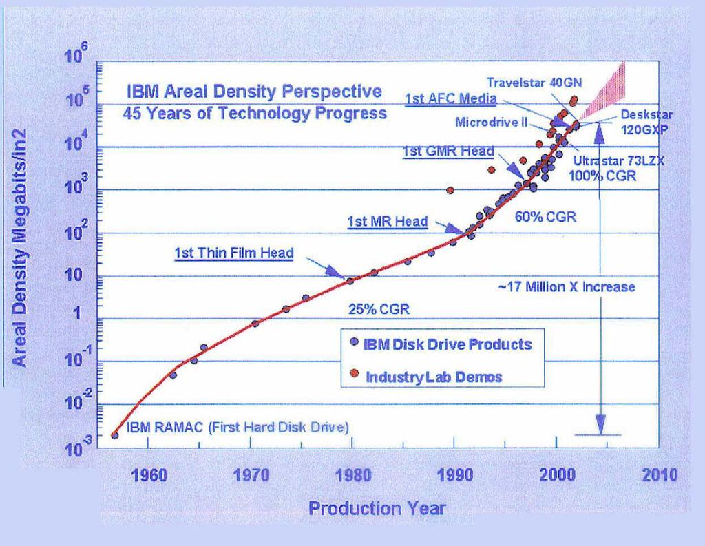
14 Magnetic Disk Storage In mid 1960 s, the storage limits was being approached hand made and assembled copper wired heads were becoming too small to promise extendibility.

15
16

17

18
19
20 First Paradigm Shift Investigation of magnetic films by electroplating [1] showed that there may be a possibility of plating magnetic material with the desired properties Replace hand fabricated heads by batch fabricated lithographically shaped heads: [2] chemical etching cannot produce pattern densities required electroplating through resist masks onto thin seed layers invented Both plating and lithography require intensive work to provide better understanding, proper tools and engineering work. 1. Magnetic Properties of Plated Films, L. T. Romankiw and D. A. Thompson (1975). 2. Pattern Generation in Metal Films Using Wet Chemical techniques, L. T. Romankiw (1976).
21 First Paradigm Shift (cont d) Build multiple 3D copper wound magnetic horse shoe structures on a substrate which would act as an inductive head. Maximize the number of Cu conductor turns in the yoke area. The semiconductor technology was just being developed, could not meet the challenge. The thick films could not be produced by dry processes. Electroplating technology had a better chance. Many new inventions and developments had to be done, understanding had to be achieved of individual steps, and process integration had to worked out. Major breakthroughs were necessary in electrochemistry, solution chemistry, electrochemical technology, engineering, tool design, process control, lithography microfabrication, dielectrics and chemical etching.

22 Inventions in the First Paradigm Shift (cont d) Permalloy plating bath and bath controls Electroplating cell with paddle agitation Plating of permalloy and of copper through mask to build 3D structures and removal of seed layer Through frame plating to achieve uniform thickness and film composition be able to use low magnetic field for anisotropy Use of AE photo resist as dielectric Chemical etching of extra permalloy Magnetic annealing and stabilization of permalloy Correlation had to be developed between the plating solution, film nucleation and growth, intrinsic properties of plated films and performance of the head
23 Effect of the Inventions The inventions and developments in electrochemical technology resulted in heads that not only gave more than one order of magnitude jump in recording density but also at much lower cost. Several breakthroughs in understanding of electrochemical technology gave a tremendous bust to electrochemistry as a potential fabrication approach for magnetic and electronic devices. Plating through mask technology proved to have much superior replication of patterns than other techniques. X-ray lithography masks, C-4 bumps, thin film packaging and others quickly adopted plating.

24

25

26 Investigated entire NiFeCo diagram


27
28
29 Second Paradigm Shift Inductive write MR (GMR) or spin valve read head: [1] read signal much larger and independent of disk speed. Made possible to greatly decrease track width and to decrease diameter of disk from 12 or 10 to 3.5, 2.5 and even 1 inch while maintaining as high as 10 to 70 Gb/in 2. The additional 3 order of magnitude jump in density gave birth to variety of portable devices extraordinary high density servers and low seek time. The cost of storage has decreased by 4 order of magnitude. The electrochemical technology has now been again challenged to come up with CoFeNi and CoFe alloys with Bs of 2.0 and 2.4 Tesla. New thin film alloys of CoFeNi and Co Fe have been plated which meet these new requirements. Experience gained, both in industry and universities, over the past 30 years, has elevated the understanding and knowledge of electrochemical technology, to the level that it is now possible to use mathematical models and tailor the magnetic properties nearly at will. Plating has become low cost preferred reliable technology, not only in storage, but in electronics in general and MEMS. 1. Integrated Magnetoresistive Read Inductive Write Head, L. T. Romankiw, US patent, 3,908,194 (1975).
30 Third Paradigm Shift Because of the superparamagnetic limits in the storage medium we are on the verge of the third major paradigm shift. Perpendicular recording opens new horizons, with a Tb/in 2 objective density. This poses new challenges to the electrochemical technologist. 3D structures with 50 nm width have been plated before. What is necessary is laminated structures which would make the magnetics favorable, and would allow very high speed switching.
31

32

33 Nickel stud plated into a 100 um photo resist pattern to 75% resist thickness


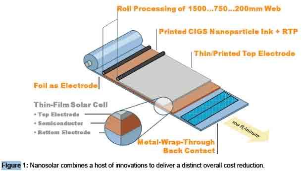
34 Ni electroplated through resist mask Top surface profile shows the equi -potential lines and the equi-concentration lines of mass flux


35 1974 first 12 um PMMA exposed using X-ray Au Mask produced by electroplating -


36 MEMS Ni parts electroplated in 1992 using X-ray lithography

37 Areas in which electrochemical technology is used today

38

39 PV PV

40

41 Typical CIS or CIGS solar cell Glass protection Transparent conductor (ZnO:AlO2 CdS Electroplated CuInS or CuInGaSe Mo back contact Ionic barrier Substrate glass or metal

42 Typical CIGS structures


43 Material issues important in the semiconductor solar absorbres Phase Adhesion Grain size Compositi on
44 Summary and conclusions 20 th Century brought the age of electronics, computers, instant communications Highly integrated silicon devices memory/logic Unprecedented increase in density and speed of magnetic recording, cost of magnetic storage far below the cost of paper storage This made Internet possible. Made visual communication, sound and information streaming possible instantly around the world. Electrochemical technology was a major contributor to the tremendous advances in technology and to drop in cost of IT.
45 Approaching the limits in silicon and magnetic storage Silicon devices as we know them today can be extended perhaps through 2025 Magnetic storage will approach the limit also in , limit smallest particle which store the information The answers will be in new surface based phenomena single layer films single rows of atoms. Bulk properties of materials will loose meaning
46 What the future holds fro electrochemical technology? Entirely new understanding will be developed of what intrinsic properties of the very thin films mean compared to bulk New understanding will have to be developed of the basics and of the properties of the new ultra thin engineering materials, new ways of device integration and new processes to fabricate devices. Electrodeposition from aqueous solutions may not be adequate plating from organic based solution may be preferred
47 What future holds (cont d) A new electromotive series based on preferred organic solvent or solvents will be needed. Mono layers and self assembled layers will not be exception they will be the roole. Electrochemistry will play a key role not only in electronic devices, IT, but even more so in solar energy conversion and storage. ELECTROCHEMICAL TECHNOLOGY HAS ABRIGHT FUTURE -
48
49