The impact of atomic layer deposition technological parameters on optical properties and morphology of Al 2 O 3 thin films
|
|
|
- Shana Jones
- 5 years ago
- Views:
Transcription
1 Optica Applicata, Vol. XLV, No. 4, 5 DOI:.577/oa54 The impact of atomic layer deposition technological parameters on optical properties and morphology of Al O 3 thin films LESZEK A. DOBRZAŃSKI, MAREK SZINDLER *, MAGDALENA SZINDLER, BARBARA HAJDUK, SONIA KOTOWICZ Institute of Engineering Materials and Biomaterials, Silesian University of Technology, Konarskiego 8a, 44- Gliwice, Poland Center of Polymer and Carbon Materials, Polish Academy of Sciences, M. Curie-Sklodowskiej 34, 4-89 Zabrze, Poland * Corresponding author: marek.szindler@polsl.pl This paper presents some results of investigations on aluminum oxide Al O 3 thin films prepared by the atomic layer deposition method on polished monocrystalline silicon. It has been described how the technological parameters of the deposition process, like the number of cycles and substrate temperature, influenced the optical properties and morphology of prepared thin films. Their physical and optical properties like thickness, uniformity and refractive index have been investigated with spectroscopic ellipsometry, atomic force microscopy and UV/vis optical spectroscopy. Keywords: thin film, aluminum oxide, atomic layer deposition.. Introduction Transparent thin films deposited onto the surface of optoelectronic devices can be used as antireflective coatings. The basic application of this kind of thin films is decreasing of the reflection while the rest of parameters like transmission and emission have controlled values. The optical dependences of optoelectronic devices like transmission or emission should be contained in a 8 to nm range. Basing on intensity or/and range of the absorbed, reflected or transmitted light, the described materials are divided into active and passive groups [ 3]. The thin passive films are used as elements of optical filters, reflection and antireflection coatings. The antireflection coatings reduce the intensity of light reflected from the surface. The known and popular materials used as antireflection coatings in photovoltaics are SiO, a-sin x :H, TiO, a-si:c:h, ZnS, Ta O 5, Sn x O y, SiN x, MgF [4 7]. Aluminum trioxide has a good refractive index and excellent transparency in a wide spectral range. In addition Al O 3 shows good mechanical properties such as a ratio of resistance to mechanical damage, which has a high value [8].
2 574 M. SZINDLER et al. The deposition methods like chemical vapour deposition (CVD) and physical vapour deposition (PVD) are generally known as methods with high purification and many variable parameters like thermal sources temperature and pressure. The comparison of these methods with atomic layer deposition (ALD) proved that ALD has been the most promising preparation method of Al O 3 thin films. The growth of thin films prepared with ALD method can be easily controlled if we note that their thickness depends just on the number of cycles and substrate temperature. Regarding the chemical reaction of precursors used, we see that in the CVD and the PVD methods the reaction occurs already in the flow of reactants used. In the ALD method, the reaction occurs just on the substrate surface. The growth of thin films also does not depend on the uniformity of the flow of precursors, like in case of PVD and CVD [9 ].. Materials and methodology The Al O 3 antireflection coatings were prepared with the ALD method. As a precursor we used trimethylaluminum (TMA), water as a reactant and nitrogen as a non-reactive carrier agent. The number of cycles and the temperature of substrate were controlled during the deposition process. Basing on obtained results, we have optimized the deposition process for the controlled growth of thin films and their quality. A different, determined number of cycles was included in every thin films deposition process. The following steps have been included in one cycle. The TMA used as a precursor was injected into the reaction chamber in one pulse. In the next step, the chamber was flushed with nitrogen gas. Water vapours were injected into the reaction chamber as the second precursor. One monolayer of Al O 3 was deposited during one cycle. The reaction between TMA and H O occurs in two steps []: Al-OH * + Al( CH 3 ) 3 Al-O-Al( CH 3 )* + CH 4 Al-CH* 3 + H O Al-OH * + CH 4 () () The number of cycles was the parameter which has decided about the thickness of such prepared thin films. As substrates we have used polished silicon wafers. The technological parameters of the deposition process are shown in Tables and. The D T a b l e. The technological parameters of ALD process. TMA The flow rate of the carrier gas N 5 sccm Pulse time. s Purge time 4. s H O The flow rate of the carrier gas N sccm Pulse time. s Purge time 5. s Substrate temperature 4 C Number of cycles 63 3
 and the RMS and R a")
3 The impact of atomic layer deposition technological parameters T a b l e. The substrate temperatures and number of cycles used for individual layers. Sample Deposition temperature [ C] Number of cycles A 3 63 B 3 83 C 3 3 D 63 E 4 63 and 3D topographic μm images were performed with XE- Park Systems atomic force microscope (AFM) and the RMS and R a coefficient values were determined with XEI Software. The thickness distribution maps and refractive index dispersions were obtained with the use of a spectroscopic elipsometer SENTECH SE 85E and with SpectraRay3 software. The thickness distribution maps were generated in an elipsometer mapping mode, where the theoretical model was a base for determining the thickness values. 3. Results and discussion The AFM analysis has been performed on Al O 3 thin films, deposited onto polished silicon wafers. The topographic and sensor images of thin films obtained with 3 C substrate temperature at a variable number of cycles are shown in Figs. 3. The images performed on thin films deposited at and 4 C at a constant number of cycles are shown in Figs. 4 and 5. The values of RMS and R a coefficients are included in Table 3. The histograms of irregularities are compared in Fig. 6. It has been found that the value of RMS coefficient is decreasing with the number of cycles at constant temperature. The maximum value is equal to.96 nm for a thin film deposited with 63 cycles at 3 C substrate temperature and its lowest value is.9 nm at the same number of cycles and at C substrate temperature. The surface Fig.. The D and 3D topography of μm area of Al O 3 thin film obtained with 63 cycles at 3 C substrate temperature (sample A).

. Fig.")
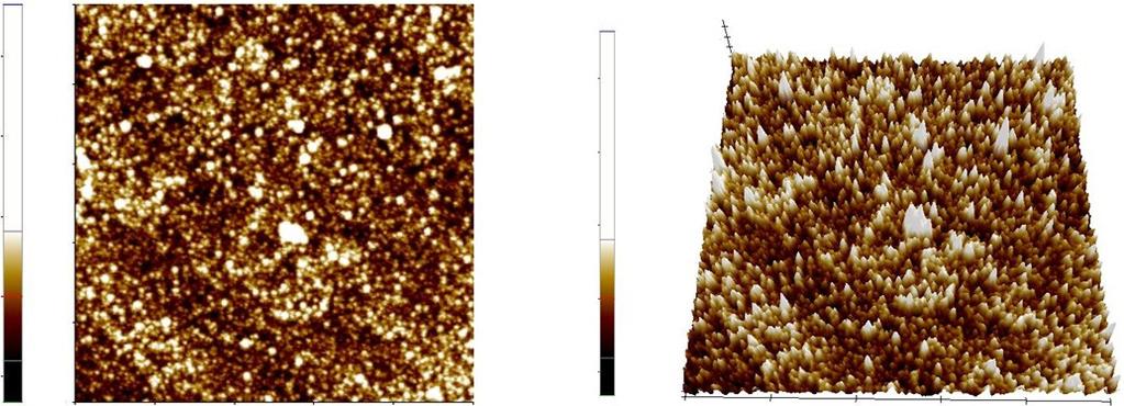
4 576 M. SZINDLER et al. Fig.. The D and 3D topography of μm area of Al O 3 thin film obtained with 83 cycles at 3 C substrate temperature (sample B) Fig. 3. The D and 3D topography of μm area of Al O 3 thin film obtained with 3 cycles at 3 C substrate temperature (sample C). Fig. 4. The D and 3D topography of μm area of Al O 3 thin film obtained with 63 cycles at C substrate temperature (sample D).

5 The impact of atomic layer deposition technological parameters Fig. 5. The D and 3D topography of μm area of Al O 3 thin film obtained with 63 cycles at 4 C substrate temperature (sample E). roughness does not increase with increasing temperature. It may be connected with the so-called temperature window in the ALD process. For thermal ALD processes there are temperature constraints on the feasibility of successfully carrying out a par- T a b l e. 3. Values of thickness d, RMS and R a coefficients for individual films. Sample Number of cycles T [ C] d RMS R a A B C D E Sample: E Number of pixels 6 B C D A Height Fig. 6. The histogram of frequencies with the occurred heights for Al O 3 thin films deposited after 63 cycles (sample A), 83 cycles (sample B) and 3 cycles (sample C) at 3 C, and thin films obtained with 63 cycles at C (sample D) and 4 C (sample E).

6 578 M. SZINDLER et al. ticular deposition. If the temperature is very high, then the first chemical reactant may decompose on the surface before having time to react with the second reactant. In this case, the growth rate would be higher than one would expect from an ALD process. Alternately, if the first precursor is stable, it may still desorb from the surface before having a chance to react with the second reactant. Under this circumstance, the growth rate would be less than expected and irregular. On the other hand, if the temperature is too low, we may adsorb more than one monolayer per cycle (or even condense a liquid or solid on the surface), and the deposition rate would be higher than expected. Finally, if the temperature is too low, the reaction rate may be so slow that the reaction time may be too long compared to a practical cycle time. In this case, there may not be enough time for a complete monolayer to be reacted. Determining, contributing and confirmation of this thesis require further research and analysis. The profile analysis represented by R a value has confirmed the decreasing tendency of RMS. With higher number of cycles the thickness of films is increasing and the surface of obtained thin films is smoother if we regard the microscopic scale. According to roughness coefficients analysis, the performed images show the surface changes and when the RMS value is higher, the area of small aggregations is visible in topographies. The histograms obtained with AFM microscope software present the number of pixels with different height depending on its value. That corresponds with the area occupied with the highest and lowest points. The obtained histograms are in good coincidence with RMS values. All samples were scanned with a spectroscopic elipsometer equipped with microspots, where the diameter of the light beam is at about μm. The thickness distribution maps were performed in 5 points on.5.5 cm area. The maps are presented in Figs. 7. X [mm] Surface [%] Y [mm] Fig. 7. The thickness distribution map of a sample A deposited with 63 cycles at 3 C substrate temperature.
![The impact of atomic layer deposition technological parameters... 579 X [mm] Surface [%] 5..5.5 5. 5 5. 89](/docs-images/89/98749290/images/7-0.jpg ".5 Y [mm].5 89.5 89..5 5. 88.75 Fig. 8. The thickness distribution map of a sample B deposited with 83 cycles at 3 C substrate temperature. X [mm] Surface [%] 5..5.5 5. 5. 9.")
![5.5 9.5 Y [mm] 9. 8.75.5 5. 8.5 8.5 8. Fig. 9. The thickness distribution map of a sample C deposited with 3 cycles at 3 C substrate temperature.](/docs-images/89/98749290/images/7-1.jpg "The obtained results show very clearly that the quality of obtained thin films was very good even in a macroscopic scale. The thickness value variation was not high. We can see in Fig.")
7 The impact of atomic layer deposition technological parameters X [mm] Surface [%] Y [mm] Fig. 8. The thickness distribution map of a sample B deposited with 83 cycles at 3 C substrate temperature. X [mm] Surface [%] Y [mm] Fig. 9. The thickness distribution map of a sample C deposited with 3 cycles at 3 C substrate temperature. The obtained results show very clearly that the quality of obtained thin films was very good even in a macroscopic scale. The thickness value variation was not high. We can see in Fig. 7 that thickness variation (the difference between the lowest and the maximum value of thickness) was.5,.75 and.5 nm in Figs. 8 and 9, respectively. At a bigger number of cycles also the percentage of uniform area with a constant thickness value is higher. The quality of scanned thin films deposited at different temperatures of the substrate ( and 4 C) showed in Figs. and is comparable with the results presented above. The thickness variations of obtained maps was equal to.4 and.9 nm.
![58 M. SZINDLER et al. X [mm] Surface [%] 5..5.5 5. 5. 5.7.5 5.6 Y [mm] 5.5.5 5. 5.4 5.3 Fig.. The thickness distribution map of a sample D deposited with 63 cycles at C substrate temperature.](/docs-images/89/98749290/images/8-0.jpg "X [mm] Surface [%] 5..5.5 5. 5 5..5 7.9 7.8 7.7 Y [mm].5 7.6 7.5 7.4 7.3 7. 7. 5. 7 Fig.. The thickness distribution map of a sample E deposited with 63 cycles at 4 C substrate temperature.")

8 58 M. SZINDLER et al. X [mm] Surface [%] Y [mm] Fig.. The thickness distribution map of a sample D deposited with 63 cycles at C substrate temperature. X [mm] Surface [%] Y [mm] Fig.. The thickness distribution map of a sample E deposited with 63 cycles at 4 C substrate temperature. The dispersions of the refractive index were determined with SpectraRay3 Software basing on a constructed model. Thin films of Al O 3 deposited onto silicon wafers were fitted with a simple sandwich model Si/SiO /Al O 3 /air. In the case of Al O 3 thin films, the Cauchy model was used. This model is most often used for transparent oxide materials. The model includes layers of SiO having a thickness of.45 nm found on the surface of silicon. The thickness of the oxide layer was determined based on an analysis of the uncovered silicon substrates. The dependences on wavelength are showed in Fig.. The comparison of refractive index dispersions shows that the value n is slightly different in UV-vis range and begins to be constant in the IR, where it is equal to.6.
9 The impact of atomic layer deposition technological parameters Refractive index n Sample: A C B D E Wavelength Fig.. Dispersion of refractive index of Al O 3 thin film. If we compare the value n for 63 nm wavelength, we note that dispersions of samples C and D layers are the same in all ranges. The values of the refractive index noted at about 63 nm are showed in Table 4. The refractive index value depends on a sample structure. Similar values of refractive index suggest that both of these features are comparable in all obtained thin films, however the refractive index value is slightly different than in [] where the value n is increasing with the temperature of the substrate. The reflectance spectra were performed on Al O 3 thin films deposited onto polished monocrystalline silicone wafers. One can see that minima of obtained spectra are shift- T a b l e 4. Refractive index values of Al O 3 thin films. Sample A B C D E n Reflectance [%] Sample: A B C D E Wavelength Fig. 3. The spectrum of reflection for the Al O 3 thin film deposited with ALD method.
10 58 M. SZINDLER et al. ed into higher wavelength values. The reflectance spectra depend on the thickness and refractive index (which depend on the technical parameters of deposition process). One can see that minima of reflectance spectra of samples A, B and C films are placed at about 475, 6 and 75 nm what agrees with their thickness and with the number of cycles. The minima of samples D and E spectra are placed at about 55 and 63 nm what is also connected with their thickness and temperature of substrate during the deposition process. And it is clearly seen in Fig. 3 that spectra B and E got minimum placed at about 6 and 64 nm, respectively. 4. Conclusions Thin films of Al O 3 were prepared with the ALD deposition method in two ways, where the first one was connected with increasing number of cycles and the second one with different temperature of a substrate during the deposition process. Basing on obtained results, we have found that the best optical and physical properties present layers prepared at 3 and 4 C substrate temperature at 83 and 63 cycles. The mentioned thin films prepared under these conditions have reduced the reflection significantly under 5% over a broad spectral range. Also the uniformity of these samples is very high and the thickness profile across all its volume is not higher than nm. Basing on obtained results, we can conclude that Al O 3 thin films obtained with the ALD deposition method have good antireflection properties and could be applied in photovoltaic industry as an antireflection coating of silicon solar cells. References [] DOMARADZKI J., BORKOWSKA A., KACZMAREK D., PROCIÓW E.L., Properties of transparent oxide thin films prepared by plasma deposition, Optica Applicata 35(3), 5, pp [] BORKOWSKA A., DOMARADZKI J., KACZMAREK D., Influence of Eu dopant on optical properties of TiO thin films fabricated by low pressure hot target reactive sputtering, Optica Applicata 37( ), 7, pp. 7. [3] MAZUR M., WOJCIESZAK D., DOMARADZKI, J., KACZMAREK D., SONG S., PLACIDO F., TiO /SiO multilayer as an antireflective and protective coating deposited by microwave assisted magnetron sputtering, Opto-Electronics Review (), 3, pp [4] JONG-HONG LU, JEN-WEI LUO, SHIOU-RUEI CHUANG, BO-YING CHEN, Antireflection coatings with SiO x -TiO multilayer structures, Japanese Journal of Applied Physics 53(S), 4, article RA6. [5] CHANG G.K., Antireflection layer coatings on the Si solar cell using SiO and Si 3 N 4, Materials Science Forum 449(4), 4, pp [6] KEDAWAT G., SRIVASTAVA S., KUMAR JAIN V., KUMAR P., KATARIA V., AGRAWAL Y., KUMAR GUPTA B., VIJAY Y.K., Fabrication of artificially stacked ultrathin ZnS/MgF multilayer dielectric optical filters, ACS Applied Materials and Interfaces 5(), 3, pp [7] LIPINSKI M., ZIEBA P., JONAS S., KLUSKA S., SOKOŁOWSKI M., CZTERNASTEK H., Optimisation of SiN x :H layer for multicrystalline silicon solar cell, Opto-Electronics Review (), 4, pp [8] DOBRZAŃSKI L.A., SZINDLER M., DRYGAŁA A., SZINDLER M.M., Silicon solar cells with Al O 3 antireflection coating, Central European Journal of Physics (9), 4, pp
11 The impact of atomic layer deposition technological parameters [9] LESKELÄ M., RITALA M., Atomic layer deposition (ALD): from precursors to thin film structures, Thin Solid Films 49(),, pp [] SNEH O., CLARK-PHELPS R.B., LONDERGAN A.R., WINKLER J., SEIDEL T.E., Thin film atomic layer deposition equipment for semiconductor processing, Thin Solid Films 4( ),, pp [] SEIDEL T., LONDERGAN A., WINKLER J., XINYE LIU, RAMANATHAN S., Progress and opportunities in atomic layer deposition, Solid State Technology 46(5), 3, pp [] GRONER M.D., FABREGUETTE F.H., ELAM J.W., GEORGE S.M., Low-temperature Al O 3 atomic layer deposition, Chemistry of Materials 6(4), 4, pp Received April, 5 in revised form June 9, 5