Chapter 4. Introduction to Dislocations
|
|
|
- Wilfrid Foster
- 5 years ago
- Views:
Transcription
1 Chapter 4 Introduction to Dislocations The discrepancy between the theoretical and observed yield stresses of crystals Dislocations The Burgers vector Vector notation for dislocations Dislocations in the face-centered cubic lattice Intrinsic and extrinsic stacking faults in face-centered cubic metals Extended dislocations in hexagonal metals Climb of edge dislocations Dislocation interactions The stress field of a screw dislocation The stress field of an edge dislocation The force on a dislocation The strain energy of a screw dislocation The strain energy of an edge dislocation 1

2 Discrepancy between Theoretical & Observed Yield Stresses Discrepancy between the theoretical and observed yield stresses of crystals - The stress-strain curve of a typical magnesium single crystal, oriented with the basal plane inclined at 45 to the stress axis and strained in tension, is shown in Fig At the low tensile stress of 0.7 MPa, the crystal yields plastically and then easily stretches out to a narrow ribbon which may be 4 or 5 times longer than the original crystal. - If one examines the surface of the deformed crystal, markings can be seen which run more or less continuously around the specimen in the form of ellipses (Fig. 4.2) Fig. 4.1 Tensile stress-strain curve for a Mg single crystal. Fig. 4.2 Slip 2lines on Mg crystal.
3 Discrepancy between Theoretical & Observed Yield Stresses (A) (B) - These markings (in Fig. 4.2) recognized as a series of fine steps that have formed on the surface. The nature of these steps is shown schematically in Fig Evidently, as a result of the applied force, the crystal has been sheared on a number of parallel planes. Crystallographic analyses of the markings, furthermore, show that these are basal (0002) planes and, therefore, the closest packed plane of the crystal. - When this type of deformation occurs, the crystal is said to have undergone slip, the visible markings on the surface are called slip lines, or slip traces, and the crystallographic plane on which the shear has occurred is called the slip plane ( 滑移面 ). - The shear stress at which plastic flow begins in a single crystal is amazingly small when compared to the theoretical shear strength of a perfect crystal. Fig. 4.3 (A) Magnified schematic view of slip lines (side view). (B) Magnified schematic view of slip lines (front view) 3
4 Discrepancy between Theoretical & Observed Yield Stresses - An estimate of the strength can be obtained in the following manner. Fig. 4.4A shows 2 adjacent planes of a hypothetic crystal. A shearing stress, acting as indicated by the vectors marked,ends to move the atoms of the upper plane to the left. Each atom of the upper plane rises to a maximum position (Fig. 4.4B) as it slides over its neighbor in the plane below. This maximum position represents a saddle point. A shear of one atomic distance requires that the atoms of the upper plane in Fig. 4.4A be brought to a position equivalent to that in Fig. 4.4B, after which they move on their own accord into the next equilibrium position, Fig. 4.4C. Since the separation of the 2 planes is of the order of 2 atomic radii, the shear strain at the saddle point is approximately equal to one half. where is shear strain. a 2a 1 2 (4.1) 4
5 Discrepancy between Theoretical & Observed Yield Stresses (A) (B) (c) Fig. 4.4 (A) Initial position of the atoms on a slip plane. (B) The saddle point for the shear of one plane of 5 atoms over another. (C) Final position of the atoms after shear by one atomic distance.
6 Discrepancy between Theoretical & Observed Yield Stresses - In a perfectly elastic crystal, the ratio of shear stress to shear strain is equal to the shear modulus: (4.2) where is shear strain, is shear stress, and is shear modulus. - Substituting the value ½ for the shear strain, and the value 17.2 GPa for, which is of the order of magnitude of the shear modulus for magnesium, we obtain for the stress at the saddle point, ,200MPa MPa - Real crystals deform at small fractions of their theoretical strengths (1/1000 to 1/100,000). 0.7MPa MPa 3 6
7 Dislocations Dislocations ( 差排, 錯位 ) - The discrepancy between the computed and real yield stresses is because real crystals contain defects. - If the transmission foil has been prepared properly and contains a section of a slip plane, where it is examined in the microscope one may obtain a photograph of the type shown schematically in Fig. 4.5A. The lines (a-a and b-b) have been drawn on the figure to indicate the positions where the slip plane intersects the foil surfaces. - It should be noted that the drawing in Fig. 4.5A is a 2- dimensional projection of a 3-dimensional specimen. - Fig. 4.5 B demonstrates that the dark lines in the photograph run across the slip plane from the top to the bottom surfaces of the foil. - In a crystal which has undergone slip, lattice defects tend to accumulate along the slip planes. These defects are called dislocations. Fig. 4.5(A) 7
8 Dislocations - The points where dislocations intersect a specimen surface can often be made visible by etching the surface with a suitable etching solution. As a result, etch pits may form (Fig. 4.5C). (A) (B) (C) Fig. 4.5 (A) Schematic representation of an electron microscope photograph showing a section of a slip plane. (B) A 3-dimensional view of the same slip plane section. (C) Termination of dislocations can also be revealed by etch pits. 8


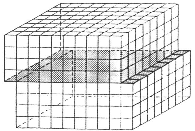
9 Dislocations - Fig. 4.6 shows a portion of a foil of an aluminum specimen with a grain containing a slip plane with dislocations. The specimen was polycrystalline. The dark region at the upper right-hand corner represents a second grain. - The best evidence now indicates that dislocations are boundaries on the slip planes where a shearing operation has ended. Fig. 4.6 An electron micrograph of a foil removed from an aluminum specimen. Note the dislocations lying along a slip plane, in agreement with Fig
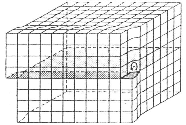
10 Dislocations Edge dislocation ( 刃差排 ) - Fig. 4.7A represents a simple cubic crystal that is assumed to be subjected to shearing stresses,, on its upper and lower surfaces. The line SP represents a possible slip plane in the crystal. As a result of the applied shear stress, the righthand half of the crystal is displaced along SP so that the part above the slip plane is moved to the left with respect to the part below the slip plane. The amount of this shear is assumed to equal one interatomic spacing in a direction parallel to the slip plane. - As may be seen in Figs. 4.7B and C, this will leave an extra half-plane cd below the slip plane at the right and outside the crystal. It will also form an extra vertical halfplane ab above the slip plane and in the center of the crystal. - Fig. 4.7B clearly shows that the crystal is badly distorted where this half-plane terminates at the slip plane. It can also be deduced that this distortion decreases in intensity as one moves away from the edge of this half-plane. This is because at large distances from this lower edge of the extra plane, the atoms tend to be arranged as they would be in a perfect crystal. The distortion in the crystal is centered around the edge of the extra plane. This boundary of the additional plane is 10 called an edge dislocation.
 A perfect crystal.")

11 (A) Dislocations (B) (C) Fig. 4.7 An edge dislocation. (A) A perfect crystal. (B) When the crystal is sheared one atomic distance over part of the distance S-P, an edge dislocation is formed. (C) 3 dimensional view of slip. 11


12 Dislocations - Fig. 4.8 represents a 3-dimensional sketch of the edge dislocations of Fig The figure clearly shows that the dislocation has the dimensions of a line. Another important fact is that the dislocation line marks the boundary between the sheared and unsheared parts of the slip plane. - In fact, a dislocation may be defined as a line that forms a boundary on a slip plane between a region that has slipped and one that has not. Fig. 4.8 This 3-dimensional view of a crystal containing an edge dislocation shows that the dislocation forms the boundary on the slip plane between a region that has been sheared and a region that has not been sheared. 12
13 Dislocations - As a result of the applied stress, atom c in Fig. 4.9A may move to the position marked c in Fig. 4.9B. The final result is that the crystal is sheared across the slip plane by one atomic distance, as shown in Fig. 4.9C. - Each step in the motion of the dislocation (Fig. 4.9) requires only a slight rearrangement of the atoms in the neighborhood of the extra plane. As a result, a very small force will move a dislocation. - In 1934, Orowan, Polyani, and Taylor presented papers which are said to have laid the foundation for the modern theory of slip due to dislocations. (A) (B) (C) Fig. 4.9 Three stages in the movement of an edge dislocation through a crystal. 13
14 Dislocations Screw dislocation ( 螺旋差排 ) - The movement of a single dislocation completely through a crystal produces a step on the surface, the depth of which is one atomic distance. Many hundreds or thousands of dislocations must move across a slip plane in order to produce a visible slip line. - Fig. 4.10A shows a screw dislocation, where each small cube can be considered to represent an atom. Fig. 4.10B represents the same crystal with the position of the dislocation line marked by the line DC. (A) (B) Fig Two representations of a screw dislocation. Notice that the planes in this dislocation spiral around the dislocation like a left-hand screw. 14
15 Dislocations - The designation screw for this lattice defect is derived from the fact that the lattice planes of the crystal spiral the dislocation line DC. This statement can be proved by starting an point x in Fig. 4.10A and then proceeding upward and around the crystal in the direction Fig. 4.10(A) of the arrows. One circuit of the crystal ends at point y; continued circuits will finally end at point z. - Fig. 4.10B plainly shows that a dislocation in a screw orientation also represents the boundary between a slipped and an unslipped area. Here the dislocation, centered along line DC, separates the slipped area ABCD from the remainder of the slip plane in back of the dislocation. Fig. 4.10(B) 15


16 Materials Science and Engineering Dislocations-Linear Defects Dislocation line could be seen as a line to separate the deformed and undeformed regions. Figure 4.4 (a) A screw dislocation within a crystal. (b) The screw dislocation in (a) as viewed from above. The dislocation line extends along line AB. Atom positions above 16 the slip plane are designated by open circles, those below by solid circles.
17 Dislocations Dislocations - The edge dislocation shown in Fig. 4.7B has an incomplete plane which lies above the slip plane. It is also possible to have the incomplete plane below the slip plane. The 2 cases are differentiated by calling the former a positive edge dislocation, and the latter a negative edge dislocation. Fig. 4.7(B) Symbols representing these 2 forms are and, respectively, where the horizontal line represents the slip plane and the vertical line the incomplete plane. - The screw dislocation shown in Fig has lattice planes that spiral the line DC like a left-hand screw. - Both forms of the edge and the screw dislocations, respectively, are shown in Fig Fig. 4.10(B) 17
18 Materials Science and Engineering Dislocations-Linear Defects Positive edge dislocation Negative edge dislocation 18
19 Dislocations (A) (B) (C) (D) Fig The ways that the 4 basic orientations of a dislocation move under the same applied stress: 19 (A) Positive edge, (B) Negative edge, (C) Left-hand screw, and (D) Right-hand screw.
20 Dislocations - Fig shows that a positive edge dislocation moves to the left when the upper half of the lattice is sheared to the left. On the other hand, a negative edge dislocation moves to the right, but produces the identical shear of the crystal. The right-hand screw moves forward and the left-hand screw moves to the rear, again producing the same shear of the lattice. - Dislocations cannot end inside a crystal. - In Fig. 4.13, the 2 dislocation segments a and b form a continuous path through the crystal from front to top surfaces. Fig Dislocations can vary in direction. This shaded extra plane forms a dislocation with edge components a and b. 20
21 Dislocations - It is also possible for all 4 edges of an incomplete plane to lie inside a crystal, forming a 4-sided closed edge dislocation at the boundaries of the plane. - Furthermore, a dislocation that is an edge in one orientation can change to a screw in another orientation, as is illustrated in Figs and Fig A 2-component dislocation composed of an edge and a screw component. Fig Atomic configuration corresponding to the dislocation of Fig viewed from above. Opencircle atoms are above the slip plane, dot atoms are below the slip plane. 21
22 Dislocations - A dislocation does not need to be either pure screw or pure edge, but may have orientations intermediate to both. Fig shows a change in orientation from edge to screw, but here the change is not abrupt. - Fig consists of the 4 elementary types of dislocations. Sides a and c are positive and negative edge dislocations, respectively, while b and d are right- and left-hand screws, respectively. Fig A closed dislocation loop consisting of (a) positive edge, (b) right-hand screw, (c) negative edge, and (d) left-hand screw. Fig A dislocation that changes its orientation from a screw to an edge as viewed from above looking down on its slip plane. 22
23 Dislocations - A dislocation cannot inside a crystal. This is because a dislocation represents the boundary between a slipped and an unslipped area. - If the slipped area on the slip plane does not touch the specimen surface, as in Fig. 4.18, then its boundary is continuous and the dislocation has to be a closed loop. Fig A curved dislocation loop lying in a slip plane. 23
24 Burgers Vector The Burgers vector - In Fig. 4.17, although the dislocation varies in orientation in the slip plane ABCD, the variation in shear across the dislocation is everywhere the same, and the slip vector b is therefore a characteristic property of the dislocation. By definition, this vector is called the Burgers vector of the dislocation. - The Burgers vector of a dislocation is an important property of a dislocation because, if the Burgers vector and the orientation of the dislocation line are known, the dislocation is completely described. Fig
25 Burgers Vector - In Fig. 4.19A a counterclockwise circuit of atom-to-atom steps in a perfect crystal closes, but when the same step-by-step circuit is made around a dislocation in an imperfect crystal (Fig. 4.19B), the end point of the circuit fails to coincide with the starting point. The vector b connecting the end point with the starting point is the Burgers vector of the dislocation. (A) (B) 25 Fig The Burgers circuit for an edge dislocation: (A) Perfect crystal and (B) crystal with dislocation.
26 Burgers Vector - The procedure can be used to find the Burgers vectors of any dislocation if the following rules are observed: 1. The circuit is traversed in the same manner as a rotating right-hand screw advancing in the positive direction of the dislocation. 2. The circuit must close in a perfect crystal and must go completely around the dislocation in the real crystal. 3. The vector that closes the circuit in the imperfect crystal (by connecting the end point to the starting point) is the Burgers vector. - The above convention involving a right-hand (RH) circuit around the dislocation line yields a Burgers vector pointing from the finish to the start (FS) of the circuit, and because the closure failure is measured in an imperfect crystal, it is called a local Burger vector or more completely a RHFS local Burgers vector. 26
27 Burgers Vector - Fig shows a Burgers circuit around a left-hand screw dislocation. In Fig. 4.20A, the circuit is indicated for the perfect crystal. Fig. 4.20B shows the same circuit transferred to a crystal containing a screw dislocation. (A) (B) Fig The Burgers circuit for a dislocation in a screw orientation. (A) Perfect crystal and (B) crystal with dislocation. 27
28 Burgers Vector Characteristics of both edge and screw dislocations - Edge dislocation 1. An edge dislocation lies perpendicular to its Burgers vector. 2. An edge dislocation moves (in its slip plane) in the direction of the Burgers vector (slip direction). Under a shear-stress sense a positive dislocation moves to the right, a negative one to the left. - Screw dislocation 1. A screw dislocation lies parallel to its Burgers vector. 2. A screw dislocation moves (in the slip plane) in a direction perpendicular to the Burgers vector (slip direction). 28

29 Materials Science and Engineering Dislocations-Linear Defects Edge dislocation Dislocation line Burgers vector Slip direction Screw dislocation Dislocation line Burgers vector Slip direction 29
30 Burgers Vector Slip plane ( 滑移面 ) - The slip plane is the plane containing both the Burgers vector and the dislocation. - The slip plane of an edge dislocation is thus uniquely defined because the Burgers vector and the dislocation are perpendicular. - The slip plane of a screw dislocation can be any plane containing the dislocation because the Burgers vector and dislocation have the same direction. - Edge dislocations are confined to move or glide in a unique plane, but screw dislocations can glide in any direction as long as they move parallel to their original orientation. 30
31 Vector Notation for Dislocations Vector notation for dislocations - In any crystal form, the distance between atoms in a close-packed direction corresponds to the smallest shear distance that will preserve the crystal structure during a slip movement. Dislocations with Burgers vectors equal to this shear are energetically the most favored in a given crystal structure. - With regard to the vector notation, the direction of a Burgers vector can be represented by the Miller indices of its direction, and the length of the vector can be expressed by a suitable numerical factor placed in front of the Miller indices. - In a simple cubic lattice, the distance between atoms in a close-packed direction equals the length of one edge of a unit cell. A dislocation with a Burgers vector in a simple cubic lattice is represented by [100]. 31
32 Vector Notation for Dislocations - In Fig. 4.21, the close-packed direction in a face-centered cubic lattice is a face diagonal, and the distance between atoms in this direction is equal to one-half the length of the face diagonal. As a result, a dislocation in a face-centered cubic lattice having a Burgers vector lying in the [101] direction should be written ½[101]. - In the body-centered cubic lattice, the close-packed direction is a cube diagonal, or a direction of the form <111>. The distance between atoms in these directions is onehalf the length of the diagonal, so that a dislocation having a Burgers vector parallel to [111] is written ½[111] Fig The spacing between atoms in the close-packed directions of the different cubic systems: face-centered cubic, body-centered cubic, and simple cubic


33 Dislocations in the Face-Centered Cubic Lattice Dislocations in the face-centered cubic lattice - The primary slip plane in the face-centered cubic lattice is the octahedral plane {111}. Fig shows a plane of this type looking down on the extra plane of an edge dislocation. Notice that in the latter plane a zigzag row of atoms is missing. This corresponds to the missing plane of the edge dislocation. Fig A total dislocation (edge orientation) in a face-centered cubic lattice as viewed when looking down on the slip plane. 33
![Dislocations in the Face-Centered Cubic Lattice - The vector b represents the Burgers vector of the dislocation, which is designed as ½[110] (Fig. 4.24).](/docs-images/83/87091838/images/34-0.jpg "As is to be expected, this dislocation movement shears the upper half of the crystal (above the plane of the paper) one unit b to the right relative to the bottom half (below the plane of the paper).")
34 Dislocations in the Face-Centered Cubic Lattice - The vector b represents the Burgers vector of the dislocation, which is designed as ½[110] (Fig. 4.24). As is to be expected, this dislocation movement shears the upper half of the crystal (above the plane of the paper) one unit b to the right relative to the bottom half (below the plane of the paper). - In Fig. 4.22, the movement of a zigzag plane of atoms, such as aa, through the horizontal distance b would involve a very large lattice strain, because each white atom at the slip plane would be forced to climb over the dark atom below it and to its right. - What actually is believed to happen is that the indicated plane of atoms makes the move indicated by the vectors marked c in Fig This movement can occur with a much smaller strain of the lattice. A second movement of the same type, indicated by the vectors marked d, brings the atoms to the same final positions as the single displacement b of Fig Fig. 4.22


35 Dislocations in the Face-Centered Cubic Lattice - The atom arrangement of Fig is particularly significant because it shows how a single-unit dislocation can break down into a pair of partial dislocations. - In Fig. 4.24, the Burgers vector of the total dislocation equals the distance B 1 B 2, while the Burgers vectors of the 2 partial dislocations c and d of Fig are the same as the distance B 1 C and CB 2. The Burgers vector of the total dislocation is ½[110]. The B 1 C lies in the [121] direction. Since B 1 C is just one-third of line mn, the Burgers vector for this partial dislocation, c, is 1/6[121]. In the same manner, the partial dislocation, d, can be represented as 1/6[211] [110] /2 1 /2 1 /21 1 / Fig Partial dislocation in a face-centered cubic lattice. Fig The orientation relationship between the Burgers vectors of a 35 total dislocation and its partial dislocations.
36 Dislocations in the Face-Centered Cubic Lattice - The total face-centered cubic dislocation ½[110] is thus able to dissociate into 2 partial dislocations according to the relation (4.4) - When a total dislocation breaks down into a pair of partials, the strain energy of the lattice is decreased. This results because the energy of a dislocation is proportional to the square of its Burgers vector and because the square of the Burgers vector of the total dislocation is more than twice as large as the square of the Burgers vector of a partial dislocation
37 Dislocations in the Face-Centered Cubic Lattice - A total dislocation that has dissociated into a pair of separated partials like those in Fig is known as an extended dislocation ( 擴展差排 ). - If we assume that the dark-colored atoms occupy A positions in a stacking sequence and the white atoms at either end of the figure, B positions, then the white atoms between the 2 partial dislocations lie on C positions. In this region, the ABCABCABC stacking sequence of the face-centered cubic lattice suffers a discontinuity and becomes ABCA CABCA. The arrows indicate the discontinuity. - Discontinuity in the stacking order of the {111}, or closepacked planes, are called stacking faults ( 疊差 ). Fig An extended dislocation. 37


38 Dislocations in the Face-Centered Cubic Lattice - The stacking fault occurs on the slip plane (between the dark and white atoms) and is bounded at its end by what are known as Shockley partial dislocations. - In all cases, if a stacking fault terminates inside a crystal, its boundaries will form a partial dislocation. - The partial dislocations of stacking faults, in general, may be either of the Shockley type, with the Burgers vector of the dislocation lying in the plane of the fault, or of the Frank type, with the Burgers vector normal to the stacking fault. Fig


39 Dislocations in the Face-Centered Cubic Lattice - The defect marked by A in Fig shows stacking faults bordered by 2 dislocations in the lower-left- and upper-right-hand side. - The defect marked by B shows a narrow region of stacking fault surrounded by Shockley partial dislocations. Fig An electron micrograph of a thin foil of lightly deformed Cu at.% Al alloy. The beam direction is close to [101] and g is indicated. 44,
40 Dislocations in the Face-Centered Cubic Lattice Stacking fault ( 疊差 ) - Since the atoms on either side of a stacking fault are not at the positions they would normally occupy in a perfect lattice, a stacking fault possesses a surface energy which, in general, is small compared with that of an ordinary grain boundary, but nevertheless finite. - The stacking-fault energy plays an important part in determining the size of an extended dislocation. The larger the separation between the partial dislocations, the smaller is the repulsive force between them. On the other hand, the total surface energy associated with the stacking fault increases with the distance between partial dislocations. The separation between the 2 partials thus represents an equilibrium between the repulsive energy of the dislocations and the surface energy of the fault. - Seeger and Schoeck have shown that the separation of the partial dislocations in an extended dislocation depends on a dimensionless parameter I c/gb 2, where I is the specific surface energy of the stacking fault, c is the separation between adjoining slip planes, G is the shear modulus in the slip plane, and b is the magnitude of the Burgers vector. 40
41 Dislocations in the Face-Centered Cubic Lattice In certain face-centered cubic metals typified by aluminum, this parameter is larger than 10-2 and the separation between dislocations is only of the order of a single atomic distance. These metals are said to have high stacking-fault energies. When the parameter is less than 10-2, a metal is said to have a low stacking-fault energy. Movement of an extended dislocation - If the moving dislocation meets obstacles, such as other dislocations, or even second-phase particles, the width of the stacking fault should vary. - Thermal vibrations may also cause the width of the stacking fault to vary locally along the dislocation, the vibration being a function of time. - An extend dislocation can be pictured as a pair of partial dislocations, separated by a finite distance, which move in consort through the crystal. 41
42 Intrinsic and Extrinsic Stacking Faults in FCC Metals Intrinsic and extrinsic stacking faults in face-centered cubic metals - The movement of a Shockley partial across the slip plane of a fcc metal has been shown to produce a stacking sequence ABCA CABC. A fault of this type is called an intrinsic stacking fault. An intrinsic stacking fault may also be developed in a fcc crystal by removing part of a close-packed plane, as shown in Fig. 4.27A. Its Burgers vector is equal to one-third of a total dislocation and therefore may be written 1/3<111>. Fig. 4.27A An intrinsic stacking fault can also be formed in a face-centered cubic crystal by removing 42 part of a close-packed plane.
43 Intrinsic and Extrinsic Stacking Faults in FCC Metals - The addition of a portion of an octahedral plane produces a different type of stacking sequence which is ABCA C BCABC. In this fault (Fig. 4.27B) a plane has been inserted that is not correctly stacked with respect to the planes on either side of the fault. This type of fault is called an extrinsic or double stacking fault. The Burgers vector for the extrinsic fault, shown in Fig. 4.27B, is 1/3<111>. An extrinsic stacking fault could be formed by the precipitation of interstitial atoms on an octahedral plane. Fig. 4.27B The addition of a portion of an extra close-packed plane to a face-centered cubic crystal produces an extrinsic stacking fault. 43
44 Extended Dislocations in Hexagonal Metals Extended dislocations in hexagonal metals - In the hexagonal system, the dissociation of a total dislocation into a pair of partials on the basal plane is expressed in the following fashion: (4.5) - For the face-centered cubic system, the dissociation of a total dislocation into a pair of partials is expressed in the following fashion: (4.6) 44
45 Climb of Edge Dislocations Climb of edge dislocations - The slip plane of a dislocation is defined as the plane that contains both the dislocation and its Burgers vector. - Since the Burgers vector is parallel to a screw dislocation, any plane containing the dislocation is a possible slip plane (Fig. 4.28A). - The Burgers vector of an edge dislocation is perpendicular to the dislocation, and there is only one possible slip plane (Fig. 4.28B). (A) (B) Fig (A) Any plane containing the dislocation is a slip plane for a screw dislocation. (B) There is 45only one slip plane for an edge dislocation. It contains both the Burgers vector and the dislocation.
46 Climb of Edge Dislocations - A screw dislocation may move by slip or glide in any direction perpendicular to its self, but an edge dislocation can only glide in its single slip plane. - Fig demonstrates a positive climb of an edge dislocation and results in a decrease in size of the extra plane. - Negative climb corresponds to the opposite of the above in that the extra plane grows in size instead of shrinking. A mechanism for negative climb is illustrated in Fig (A) (B) (C) Fig Positive climb of an edge dislocation. 46
47 Climb of Edge Dislocations - Because we are removing material from inside the crystal as the extra plane itself grows smaller, the effect of positive climb on the crystal is to cause it to shrink in a direction parallel to the slip plane (perpendicular to the extra plane). Positive climb is therefore associated with a compressive strain and will be promoted by a compressive stress component perpendicular to the extra plane. - A tensile stress applied perpendicular to the extra plane of an edge dislocation promotes the growth of the plane and thus negative climb. - Slip occurs as the result of shear stress; climb as the result of a normal stress (tensile or compressive). (A) (B) Fig Negative climb of an edge dislocation. 47
48 Climb of Edge Dislocations - Both positive and negative climb require that vacancies move through the lattice, toward the dislocation in the first case and away form it in the second case. - If the concentration of vacancies and their jump rate is very low, then it is not expected that edge dislocation will climb. - Climb is a phenomenon that becomes increasingly important as the temperature rises. Slip, on the other hand, is only slightly influenced by temperature. 48
49 Dislocation Intersections Dislocation intersections - In Fig it is assumed that a dislocation has moved across the slip plane ABCD, thereby shearing the top half of the rectangular crystal relative to the bottom half by the length of its Burgers vector b. A second (vertical) dislocation, having a loop that intersects the slip plane at 2 points, is shown in Fig It is assumed that this loop is in the edge orientation where it intersects the slip plane. - The indicated displacement of the crystal (Fig. 4.31) also shears the top half of the vertical-dislocation loop relative to its bottom half by the amount of the Burgers vector b. The displacement lengthens the vertical-dislocation loop by an amount equal to the 2 horizontal steps (Fig. 4.31). Fig In the figure a dislocation is assumed to have moved across the horizontal plane ABCD and, in cutting through the vertical-dislocation loop, it forms a pair of jogs in the latter. 49
50 Dislocation Intersections This result is characteristic of the intersection of dislocations, for whenever a dislocation cuts another dislocation, both dislocations acquire steps of a size equal to the other s Burgers vector. - The first case, where the step lies in the slip plane of a dislocation, is called a kink (Fig. 4.32). The second case, where the step is normal to the slip plane of a dislocation, is called a jog (Fig. 4.33). - The kink in the edge dislocation has a screw orientation (Burgers vector parallel to line on), while the step in the screw dislocation has an edge orientation (Burgers vector normal to the line on) (Fig. 4.32). (A) Fig Dislocations with kinks that lie in the slip plane of the dislocations. (B) 50
51 Dislocation Intersections Both of these steps can easily be eliminated by moving line mn over to the position of the dashed line. This movement in both cases can occur by simple slip. Since the elimination of a step lowers the energy of the crystal by the amount of the strain energy associated with a step, it can be assumed that steps of this type may tend to disappear. - An edge and a screw dislocation, with steps normal to the primary slip plane, are shown in Fig This type of discontinuity is called a jog. (A) Fig Dislocations with jogs normal to their slip planes. (B) 51
52 Dislocation Intersections - The edge dislocation with a jog (Fig. 4.33A) is free to move on the stepped surface, for all 3 segments of the dislocation, mn, no, and op, are in a simple edge orientation with their respective Burgers vectors lying in the crystal planes that contain the dislocation segments. - The screw dislocation with a jog (Fig. 4.33B) represents quite a different case. Here the jog is an edge dislocation with an incomplete plane lying in the stepped surface. Here the jog (line no), which is an edge orientation, is not capable of gliding along the vertical surface because its Burgers vector is not in the surface of the step but is normal to it. The only way that the jog can move across the surface of the step is for it to move by dislocation climb. Fig
53 Stress Field of a Screw Dislocation Stress field of a screw dislocation - The elastic strain of a screw dislocation is shown in Fig Consider the circular Burgers circuit shown in Fig Such a path results in an advance (parallel to the dislocation line) equal to the Burgers vector b. The strain in the lattice is the advance divided by the distance around the dislocation. b 2 r (4.7) where r is the radius of the Burgers circuit. This strain is accompanied by a corresponding state of stress in the crystal. Fig Shear strain associated with a screw dislocation. 53
54 Stress Field of a Screw Dislocation - Assuming the crystals to be homogeneous isotropic bodies, the elastic stress field surrounding a screw dislocation is written: b 2 r (4.8) where id the shear modulus of the material of the crystal. - The analysis of the stress close to the center of the dislocation is extremely difficult, and no completely satisfactory theory has yet been developed. 54
IMPERFECTIONSFOR BENEFIT. Sub-topics. Point defects Linear defects dislocations Plastic deformation through dislocations motion Surface
 IMPERFECTIONSFOR BENEFIT Sub-topics 1 Point defects Linear defects dislocations Plastic deformation through dislocations motion Surface IDEAL STRENGTH Ideally, the strength of a material is the force necessary
Single vs Polycrystals
 WEEK FIVE This week, we will Learn theoretical strength of single crystals Learn metallic crystal structures Learn critical resolved shear stress Slip by dislocation movement Single vs Polycrystals Polycrystals
Lecture # 11 References:
 Lecture # 11 - Line defects (1-D) / Dislocations - Planer defects (2D) - Volume Defects - Burgers vector - Slip - Slip Systems in FCC crystals - Slip systems in HCP - Slip systems in BCC Dr.Haydar Al-Ethari
(a) Would you expect the element P to be a donor or an acceptor defect in Si?
 Would you expect the element P to be a donor or an acceptor defect in Si?") MSE 200A Survey of Materials Science Fall, 2008 Problem Set No. 2 Problem 1: At high temperature Fe has the fcc structure (called austenite or γ-iron). Would you expect to find C atoms in the octahedral
MSE 200A Survey of Materials Science Fall, 2008 Problem Set No. 2 Problem 1: At high temperature Fe has the fcc structure (called austenite or γ-iron). Would you expect to find C atoms in the octahedral
Lecture # 11. Line defects (1D) / Dislocations
 / Dislocations") Lecture # 11 - Line defects (1-D) / Dislocations - Planer defects (2D) - Volume Defects - Burgers vector - Slip - Slip Systems in FCC crystals - Slip systems in HCP - Slip systems in BCC References: 1-
Lecture # 11 - Line defects (1-D) / Dislocations - Planer defects (2D) - Volume Defects - Burgers vector - Slip - Slip Systems in FCC crystals - Slip systems in HCP - Slip systems in BCC References: 1-
Dislocations and Plastic Deformation
 Dislocations and Plastic Deformation Edge and screw are the two fundamental dislocation types. In an edge dislocation, localized lattice distortion exists along the end of an extra half-plane of atoms,
Imperfections in atomic arrangements
 MME131: Lecture 9 Imperfections in atomic arrangements Part 2: 1D 3D Defects A. K. M. B. Rashid Professor, Department of MME BUET, Dhaka Today s Topics Classifications and characteristics of 1D 3D defects
ECE236A Semiconductor Heterostructure Materials Defects in Semiconductor Crystals Lecture 6 Oct. 19, 2017
 ECE236A Semiconductor Heterostructure Materials Defects in Semiconductor Crystals Lecture 6 Oct. 19, 2017 Stacking sequence in simple crystals. Stacking faults (intrinsic, extrinsic) Twin boundaries Dislocations
Defect in crystals. Primer in Materials Science Spring
 Defect in crystals Primer in Materials Science Spring 2017 11.05.2017 1 Introduction The arrangement of the atoms in all materials contains imperfections which have profound effect on the behavior of the
Movement of edge and screw dislocations
 Movement of edge and screw dislocations Formation of a step on the surface of a crystal by motion of (a) n edge dislocation: the dislocation line moves in the direction of the applied shear stress τ. (b)
CHAPTER 4 INTRODUCTION TO DISLOCATIONS. 4.1 A single crystal of copper yields under a shear stress of about 0.62 MPa. The shear modulus of
 CHAPTER 4 INTRODUCTION TO DISLOCATIONS 4.1 A single crystal of copper yields under a shear stress of about 0.62 MPa. The shear modulus of copper is approximately. With this data, compute an approximate
Fundamentals of Plastic Deformation of Metals
 We have finished chapters 1 5 of Callister s book. Now we will discuss chapter 10 of Callister s book Fundamentals of Plastic Deformation of Metals Chapter 10 of Callister s book 1 Elastic Deformation
Material Science. Prof. Satish V. Kailas Associate Professor Dept. of Mechanical Engineering, Indian Institute of Science, Bangalore India
 Material Science Prof. Satish V. Kailas Associate Professor Dept. of Mechanical Engineering, Indian Institute of Science, Bangalore 560012 India Chapter 3. Imperfections in Solids Learning objectives:
Two marks questions and answers. 1. what is a Crystal? (or) What are crystalline materials? Give examples
 What are crystalline materials? Give examples") UNIT V CRYSTAL PHYSICS PART-A Two marks questions and answers 1. what is a Crystal? (or) What are crystalline materials? Give examples Crystalline solids (or) Crystals are those in which the constituent
UNIT V CRYSTAL PHYSICS PART-A Two marks questions and answers 1. what is a Crystal? (or) What are crystalline materials? Give examples Crystalline solids (or) Crystals are those in which the constituent
Chapter Outline Dislocations and Strengthening Mechanisms. Introduction
 Chapter Outline Dislocations and Strengthening Mechanisms What is happening in material during plastic deformation? Dislocations and Plastic Deformation Motion of dislocations in response to stress Slip
TOPIC 2. STRUCTURE OF MATERIALS III
 Universidad Carlos III de Madrid www.uc3m.es MATERIALS SCIENCE AND ENGINEERING TOPIC 2. STRUCTURE OF MATERIALS III Topic 2.3: Crystalline defects. Solid solutions. 1 PERFECT AND IMPERFECT CRYSTALS Perfect
Strengthening Mechanisms
 ME 254: Materials Engineering Chapter 7: Dislocations and Strengthening Mechanisms 1 st Semester 1435-1436 (Fall 2014) Dr. Hamad F. Alharbi, harbihf@ksu.edu.sa November 18, 2014 Outline DISLOCATIONS AND
Twins & Dislocations in HCP Textbook & Paper Reviews. Cindy Smith
 Twins & Dislocations in HCP Textbook & Paper Reviews Cindy Smith Motivation Review: Outline Crystal lattices (fcc, bcc, hcp) Fcc vs. hcp stacking sequences Cubic {hkl} naming Hcp {hkil} naming Twinning
Dept.of BME Materials Science Dr.Jenan S.Kashan 1st semester 2nd level. Imperfections in Solids
 Why are defects important? Imperfections in Solids Defects have a profound impact on the various properties of materials: Production of advanced semiconductor devices require not only a rather perfect
E45 Midterm 01 Fall 2007! By the 0.2% offset method (shown on plot), YS = 500 MPa
, YS = 500 MPa") 1.!Mechanical Properties (20 points) Refer to the following stress-strain plot derived from a standard uniaxial tensile test of a high performance titanium alloy to answer the following questions. Show
1.!Mechanical Properties (20 points) Refer to the following stress-strain plot derived from a standard uniaxial tensile test of a high performance titanium alloy to answer the following questions. Show
Chapter 7 Dislocations and Strengthening Mechanisms. Dr. Feras Fraige
 Chapter 7 Dislocations and Strengthening Mechanisms Dr. Feras Fraige Chapter Outline Dislocations and Strengthening Mechanisms What is happening in material during plastic deformation? Dislocations and
Materials and their structures
 Materials and their structures 2.1 Introduction: The ability of materials to undergo forming by different techniques is dependent on their structure and properties. Behavior of materials depends on their
3, MSE 791 Mechanical Properties of Nanostructured Materials
 3, MSE 791 Mechanical Properties of Nanostructured Materials Module 3: Fundamental Physics and Materials Design Lecture 1 1. What is strain (work) hardening? What is the mechanism for strain hardening?
Point coordinates. Point coordinates for unit cell center are. Point coordinates for unit cell corner are 111
 Point coordinates c z 111 Point coordinates for unit cell center are a/2, b/2, c/2 ½ ½ ½ Point coordinates for unit cell corner are 111 x a z 000 b 2c y Translation: integer multiple of lattice constants
Dislocations in Materials. Dislocations in Materials
 Pose the following case scenario: Consider a block of crystalline material on which forces are applied. Top Force (111) parallel with top surface Bottom Force Sum Sum of of the the applied forces give
SECTION A. NATURAL SCIENCES TRIPOS Part IA. Friday 4 June to 4.30 MATERIALS AND MINERAL SCIENCES
 NATURAL SCIENCES TRIPOS Part IA Friday 4 June 1999 1.30 to 4.30 MATERIALS AND MINERAL SCIENCES Answer five questions; two from each of sections A and B and one from section C. Begin each answer at the
Point coordinates. x z
 Point coordinates c z 111 a 000 b y x z 2c b y Point coordinates z y Algorithm 1. Vector repositioned (if necessary) to pass through origin. 2. Read off projections in terms of unit cell dimensions a,
Problems to the lecture Physical Metallurgy ( Materialkunde ) Chapter 6: Mechanical Properties
 Chapter 6: Mechanical Properties") Institut für Metallkunde und Metallphysik Direktor: Prof. Dr. rer. nat. Günter Gottstein RWTH Aachen, D-52056 Aachen Internet: http://www.imm.rwth-aachen.de E-mail: imm@imm.rwth-aachen.de Tel.: +49 241
Institut für Metallkunde und Metallphysik Direktor: Prof. Dr. rer. nat. Günter Gottstein RWTH Aachen, D-52056 Aachen Internet: http://www.imm.rwth-aachen.de E-mail: imm@imm.rwth-aachen.de Tel.: +49 241
C h a p t e r 4 : D e f e c t s i n C r y s t a l s
 C h a p t e r 4 : D e f e c t s i n C r y s t a l s...perfection's a gift of The gods, few can boast they possess it - and most Of you, my dears, don't. - Ovid, The Art of Love Chapter 4: Defects in Crystals...
Materials Science. Imperfections in Solids CHAPTER 5: IMPERFECTIONS IN SOLIDS. Types of Imperfections
 In the Name of God Materials Science CHAPTER 5: IMPERFECTIONS IN SOLIDS ISSUES TO ADDRESS... What are the solidification mechanisms? What types of defects arise in solids? Can the number and type of defects
MSE 170 Midterm review
 MSE 170 Midterm review Exam date: 11/2/2008 Mon, lecture time Place: Here! Close book, notes and no collaborations A sheet of letter-sized paper with double-sided notes is allowed Material on the exam
Module 10. Crystal Defects in Metals I. Lecture 10. Crystal Defects in Metals I
 Module 10 Crystal Defects in Metals I Lecture 10 Crystal Defects in Metals I 1 NPTEL Phase II : IIT Kharagpur : Prof. R. N. Ghosh, Dept of Metallurgical and Materials Engineering Introduction Keywords:
Chapter Outline. How do atoms arrange themselves to form solids?
 Chapter Outline How do atoms arrange themselves to form solids? Fundamental concepts and language Unit cells Crystal structures! Face-centered cubic! Body-centered cubic! Hexagonal close-packed Close packed
4-Crystal Defects & Strengthening
 4-Crystal Defects & Strengthening A perfect crystal, with every atom of the same type in the correct position, does not exist. The crystalline defects are not always bad! Adding alloying elements to a
Chapter Outline How do atoms arrange themselves to form solids?
 Chapter Outline How do atoms arrange themselves to form solids? Fundamental concepts and language Unit cells Crystal structures Face-centered cubic Body-centered cubic Hexagonal close-packed Close packed
3. Anisotropic blurring by dislocations
 Dynamical Simulation of EBSD Patterns of Imperfect Crystals 1 G. Nolze 1, A. Winkelmann 2 1 Federal Institute for Materials Research and Testing (BAM), Berlin, Germany 2 Max-Planck- Institute of Microstructure
 Defects in solids http://www.bath.ac.uk/podcast/powerpoint/inaugural_lecture_250407.pdf http://www.materials.ac.uk/elearning/matter/crystallography/indexingdirectionsandplanes/indexing-of-hexagonal-systems.html
Imperfections in the Atomic and Ionic Arrangements
 Objectives Introduce the three basic types of imperfections: point defects, line defects (or dislocations), and surface defects. Explore the nature and effects of different types of defects. Outline Point
Dislocations Linear Defects
 Dislocations Linear Defects Dislocations are abrupt changes in the regular ordering of atoms, along a line (dislocation line) in the solid. They occur in high density and are very important in mechanical
Introduction to Engineering Materials ENGR2000 Chapter 7: Dislocations and Strengthening Mechanisms. Dr. Coates
 Introduction to Engineering Materials ENGR2000 Chapter 7: Dislocations and Strengthening Mechanisms Dr. Coates An edge dislocation moves in response to an applied shear stress dislocation motion 7.1 Introduction
Chapter 7: Dislocations and strengthening mechanisms
 Chapter 7: Dislocations and strengthening mechanisms Introduction Basic concepts Characteristics of dislocations Slip systems Slip in single crystals Plastic deformation of polycrystalline materials Plastically
Chapter 8. Deformation and Strengthening Mechanisms
 Chapter 8 Deformation and Strengthening Mechanisms Chapter 8 Deformation Deformation and Strengthening Issues to Address... Why are dislocations observed primarily in metals and alloys? How are strength
Ex: NaCl. Ironically Bonded Solid
 Ex: NaCl. Ironically Bonded Solid Lecture 2 THE STRUCTURE OF CRYSTALLINE SOLIDS 3.2 FUNDAMENTAL CONCEPTS SOLIDS AMORPHOUS CRYSTALLINE Atoms in an amorphous Atoms in a crystalline solid solid are arranged
CHEM-E5225 :Electron Microscopy Imaging II
 CHEM-E5225 :Electron Microscopy Imaging II D.B. Williams, C.B. Carter, Transmission Electron Microscopy: A Textbook for Materials Science, Springer Science & Business Media, 2009. Z. Luo, A Practical Guide
The Science and Engineering of Materials, 4 th ed Donald R. Askeland Pradeep P. Phulé. Chapter 3 Atomic and Ionic Arrangements
 The Science and Engineering of Materials, 4 th ed Donald R. Askeland Pradeep P. Phulé Chapter 3 Atomic and Ionic Arrangements 1 Objectives of Chapter 3 To learn classification of materials based on atomic/ionic
9/28/2013 9:26 PM. Chapter 3. The structure of crystalline solids. Dr. Mohammad Abuhaiba, PE
 Chapter 3 The structure of crystalline solids 1 2 Why study the structure of crystalline solids? Properties of some materials are directly related to their crystal structure. Significant property differences
Chapter One: The Structure of Metals
 Fourth Edition SI Version Chapter One: The Structure of Metals 2010. Cengage Learning, Engineering. All Rights Reserved. 1.1 Importance of the structure: Structures Processing Properties Applications Classification
Introduction to Engineering Materials ENGR2000 Chapter 4: Imperfections in Solids. Dr. Coates
 Introduction to Engineering Materials ENGR000 Chapter 4: Imperfections in Solids Dr. Coates Learning Objectives 1. Describe both vacancy and self interstitial defects. Calculate the equilibrium number
Module-6. Dislocations and Strengthening Mechanisms
 Module-6 Dislocations and Strengthening Mechanisms Contents 1) Dislocations & Plastic deformation and Mechanisms of plastic deformation in metals 2) Strengthening mechanisms in metals 3) Recovery, Recrystallization
Department of Materials Science and Engineering Massachusetts Institute of Technology 3.14 Physical Metallurgy Fall 2003 Exam I
 Department of Materials Science and Engineering Massachusetts Institute of Technology 3.14 Physical Metallurgy Fall 2003 Exam I 3 2.5 2 Frequency 1.5 1 0.5 0 10 11 12 13 14 15 16 17 18 19 20 21 22 23 24
Imperfections, Defects and Diffusion
 Imperfections, Defects and Diffusion Lattice Defects Week5 Material Sciences and Engineering MatE271 1 Goals for the Unit I. Recognize various imperfections in crystals (Chapter 4) - Point imperfections
ME 254 MATERIALS ENGINEERING 1 st Semester 1431/ rd Mid-Term Exam (1 hr)
") 1 st Semester 1431/1432 3 rd Mid-Term Exam (1 hr) Question 1 a) Answer the following: 1. Do all metals have the same slip system? Why or why not? 2. For each of edge, screw and mixed dislocations, cite
1 st Semester 1431/1432 3 rd Mid-Term Exam (1 hr) Question 1 a) Answer the following: 1. Do all metals have the same slip system? Why or why not? 2. For each of edge, screw and mixed dislocations, cite
12/10/09. Chapter 4: Imperfections in Solids. Imperfections in Solids. Polycrystalline Materials ISSUES TO ADDRESS...
 Chapter 4: ISSUES TO ADDRESS... What are the solidification mechanisms? What types of defects arise in solids? Can the number and type of defects be varied and controlled? How do defects affect material
9/29/2014 8:52 PM. Chapter 3. The structure of crystalline solids. Dr. Mohammad Abuhaiba, PE
 1 Chapter 3 The structure of crystalline solids 2 Home Work Assignments HW 1 2, 7, 12, 17, 22, 29, 34, 39, 44, 48, 53, 58, 63 Due Sunday 12/10/2014 Quiz # 1 will be held on Monday 13/10/2014 at 11:00 am
Thermally Activated Mechanisms in Crystal Plasticity
 PERGAMON MATERIALS SERIES Thermally Activated Mechanisms in Crystal Plasticity by D. Caillard CEMES/CNRS-BP4347, F 31055 Toulouse Cedex J. L. Martin IPMC/EPFL-CH 1015 Lausanne 2003 PERGAMON An Imprint
Chap. 7. Intersection of Dislocations
 Chap. 7. Intersection of Dislocations Plastic Deformation of Crystal - Slip starts at a slip system having the largest Schmid factor. - A dislocation moving in slip plane will intersect other dislocations
Activation of deformation mechanism
 Activation of deformation mechanism The deformation mechanism activates when a critical amount of mechanical stress imposed to the crystal The dislocation glide through the slip systems when the required
DISLOCATIONS. Edge dislocation Screw dislocation Dislocations in crystals
 Edge dislocation Screw dislocation Dislocations in crystals Further reading DISLOCATIONS Part of Introduction to Dislocations D. Hull and D.J. Bacon Pergamon Press, Oxford (1984) Advanced reading (comprehensive)
The high temperature decrease of the critical resolved shear stress in nickel-base superalloys
 Materials Science and Engineering A319 321 (2001) 383 387 www.elsevier.com/locate/msea The high temperature decrease of the critical resolved shear stress in nickel-base superalloys M. Kolbe * Institute
Planar Defects in Materials. Planar Defects in Materials
 Classification of Defects in Solids: Planar defects: Stacking faults o {311} defects in Si o Inversion domain boundaries o Antiphase boundaries (e.g., super dislocations): analogous to partials but in
CRYSTAL STRUCTURE, MECHANICAL BEHAVIOUR & FAILURE OF MATERIALS
 MODULE ONE CRYSTAL STRUCTURE, MECHANICAL BEHAVIOUR & FAILURE OF MATERIALS CRYSTAL STRUCTURE Metallic crystal structures; BCC, FCC and HCP Coordination number and Atomic Packing Factor (APF) Crystal imperfections:
Problems. 104 CHAPTER 3 Atomic and Ionic Arrangements
 104 CHAPTER 3 Atomic and Ionic Arrangements Repeat distance The distance from one lattice point to the adjacent lattice point along a direction. Short-range order The regular and predictable arrangement
Point Defects. Vacancies are the most important form. Vacancies Self-interstitials
 Grain Boundaries 1 Point Defects 2 Point Defects A Point Defect is a crystalline defect associated with one or, at most, several atomic sites. These are defects at a single atom position. Vacancies Self-interstitials
Learning Objectives. Chapter Outline. Solidification of Metals. Solidification of Metals
 Learning Objectives Study the principles of solidification as they apply to pure metals. Examine the mechanisms by which solidification occurs. - Chapter Outline Importance of Solidification Nucleation
Fundamental concepts and language Unit cells Crystal structures! Face-centered cubic! Body-centered cubic! Hexagonal close-packed Close packed
 Fundamental concepts and language Unit cells Crystal structures! Face-centered cubic! Body-centered cubic! Hexagonal close-packed Close packed crystal structures Density computations Crystal structure
Stacking Faults and Polytypism in Opal, SiO2.nH20
 578 Acta Cryst. (1969). A25, 578 Stacking Faults and Polytypism in Opal, SiO2.nH20 BY E.A. MONROE State University of New York College of Ceramics,, Alfred, New York, U.S.A. D. B. SASS Alfred University,
sb 3 c ¼ c v _e ss ¼ D sdsb 3
 Chapter 3 Diffusional-Creep Creep at high temperatures (T T m ) and very low stresses in fine-grained materials was attributed 50 years ago by Nabarro [237] and Herring [51] to the mass transport of vacancies
Chapter 4: Imperfections (Defects) in Solids
 in Solids") Chapter 4: Imperfections (Defects) in Solids ISSUES TO ADDRESS... What types of defects exist in solids? How do defects affect material properties? Can the number and type of defects be varied and controlled?
Chapter 4: Imperfections (Defects) in Solids ISSUES TO ADDRESS... What types of defects exist in solids? How do defects affect material properties? Can the number and type of defects be varied and controlled?
9/16/ :30 PM. Chapter 3. The structure of crystalline solids. Mohammad Suliman Abuhaiba, Ph.D., PE
 Chapter 3 The structure of crystalline solids 1 Mohammad Suliman Abuhaiba, Ph.D., PE 2 Home Work Assignments HW 1 2, 7, 12, 17, 22, 29, 34, 39, 44, 48, 53, 58, 63 Due Sunday 17/9/2015 3 Why study the structure
Dr. Ali Abadi Chapter Three: Crystal Imperfection Materials Properties
 Dr. Ali Abadi Chapter Three: Crystal Imperfection Materials Properties A perfect crystal, with every atom of the same type in the correct position, does not exist. There always exist crystalline defects,
7.1 The Onset of Permanent Deformation 1
 1 Chapter 7 Dislocations 7.1 The Onset of Permanent Deformation 1 7. Dislocations The Edge Dislocation The Screw Dislocation 3 The Burgers Vector 3 Mixed Dislocations Loops 5 7.3 Dislocations in Real Crystals
Dislocations & Materials Classes. Dislocation Motion. Dislocation Motion. Lectures 9 and 10
 Lectures 9 and 10 Chapter 7: Dislocations & Strengthening Mechanisms Dislocations & Materials Classes Metals: Disl. motion easier. -non-directional bonding -close-packed directions for slip. electron cloud
Influence of Primary and Secondary Crystallographic Orientations on Strengths of Nickel-based Superalloy Single Crystals
 Materials Transactions, Vol. 45, No. 6 (2004) pp. 1824 to 1828 #2004 The Japan Institute of Metals Influence of Primary and Secondary Crystallographic Orientations on Strengths of Nickel-based Superalloy
Comprehensive first-principles study of stable stacking faults in hcp metals
 Comprehensive first-principles study of stable stacking faults in hcp metals Binglun Yin a, Zhaoxuan Wu a,b,, W. A. Curtin a a Institute of Mechanical Engineering, École Polytechnique Fédérale de Lausanne,
Condensed Matter Physics Prof. G.Rangarajan Department of Physics Indian Institute of Technology, Madras
 Condensed Matter Physics Prof. G.Rangarajan Department of Physics Indian Institute of Technology, Madras Lecture - 3 Symmetry in Perfect Solids (Continued) (Refer Slide Time: 00:26) So, the last lecture,
3. Cubic zirconia single crystals
 3.1. Structure and phase relationship of cubic zirconium dioxide 3. Cubic zirconia single crystals 3.1. Structure and phase relationship of cubic zirconium dioxide Pure zirconia (ZrO 2 ) undergoes two
Metal working: Deformation processing II. Metal working: Deformation processing II
 Module 28 Metal working: Deformation processing II Lecture 28 Metal working: Deformation processing II 1 Keywords : Difference between cold & hot working, effect of macroscopic variables on deformation
MME 2001 MATERIALS SCIENCE
 MME 2001 MATERIALS SCIENCE 1 20.10.2015 crystal structures X tal structure Coord. # Atoms/ unit cell a=f(r) APF % SC 6 1 2R 52 BCC 8 2 4R/ 3 68 FCC 12 4 2R 2 74 HCP 12 6 2R 74 Theoretical Density, knowing
Defects and Diffusion
 Defects and Diffusion Goals for the Unit Recognize various imperfections in crystals Point imperfections Impurities Line, surface and bulk imperfections Define various diffusion mechanisms Identify factors
Chapter 8 Strain Hardening and Annealing
 Chapter 8 Strain Hardening and Annealing This is a further application of our knowledge of plastic deformation and is an introduction to heat treatment. Part of this lecture is covered by Chapter 4 of
Density Computations
 CHAPTER 3 THE STRUCTURE OF CRYSTALLINE SOLIDS Fundamental Concepts 3.1 What is the difference between atomic structure and crystal structure? Unit Cells Metallic Crystal Structures 3.2 If the atomic radius
VI. THE STRUCTURE OF SOLIDS
 VI. THE STRUCTURE OF SOLIDS 6-1 MOTIVATION We have come a great distance in the last several weeks. If everything is going according to plan, you are beginning to picture engineering as the design of energy
High temperature applications
 3. CREEP OF METALS Lecturer: Norhayati Ahmad High temperature applications -Steel power plants -Oil refineries -Chemical plants High operating temperatures Engine jet ----1400 o C Steam turbine power plants:
Module #8. Defects in Crystalline Materials. READING LIST DIETER: Ch. 4, Pages
 HOMEWORK From Dieter 4-6 Module #8 Defects in Crystalline Materials READING LIST DIETER: Ch. 4, Pages 103-114 Ch. 4, Pages 103-117 in Meyers & Chawla, 1 st ed. Ch. 1, Pages 1-26 in Argon Property Structure,
STRENGTHENING MECHANISM IN METALS
 Background Knowledge Yield Strength STRENGTHENING MECHANISM IN METALS Metals yield when dislocations start to move (slip). Yield means permanently change shape. Slip Systems Slip plane: the plane on which
3. Solidification & Crystalline Imperfections
 3. Solidification & Crystalline Imperfections solidification (casting process) of metals divided into two steps (1) nucleation formation of stable nuclei in the melt (2) growth of nuclei into crystals
Objective To study the time and temperature variations in the hardness of Al-4% Cu alloy on isothermal aging.
 EXPERIMENT 8 PRECIPITATION HARDENING IN 2024 ALUMINUM Objective To study the time and temperature variations in the hardness of Al-4% Cu alloy on isothermal aging. Introduction Materials can be hardened
Chapter 1. The Structure of Metals. Body Centered Cubic (BCC) Structures
 Structures") Chapter 1 The Structure of Metals Body Centered Cubic (BCC) Structures Figure 1. The body-centered cubic (bcc) crystal structure: (a) hard-ball model; (b) unit cell; and (c) single crystal with many unit
Chapter 1 The Structure of Metals Body Centered Cubic (BCC) Structures Figure 1. The body-centered cubic (bcc) crystal structure: (a) hard-ball model; (b) unit cell; and (c) single crystal with many unit
Supplementary Materials for
 advances.sciencemag.org/cgi/content/full/4/8/eaat4712/dc1 Supplementary Materials for In situ manipulation and switching of dislocations in bilayer graphene Peter Schweizer, Christian Dolle, Erdmann Spiecker*
STATE OF SOLIDIFICATION & CRYSTAL STRUCTURE
 STATE OF SOLIDIFICATION & CRYSTAL STRUCTURE Chapter Outline Determination of crystal properties or properties of crystalline materials. Crystal Geometry! Crystal Directions! Linear Density of atoms! Crystal
A rigid model illustrating the formation of misfit dislocations at the (111) diamond/c-bn
 diamond/c-bn") Supplementary Figure 1 Rigid model describing the formation of misfit dislocations. A rigid model illustrating the formation of misfit dislocations at the (111) diamond/ interface. The red and green lattices
Supplementary Figure 1 Rigid model describing the formation of misfit dislocations. A rigid model illustrating the formation of misfit dislocations at the (111) diamond/ interface. The red and green lattices
DEFORMATION AND FRACTURE LAB COURSE. The Bauschinger Effect
 Lab Course on Deformation and Fracture Bauschinger Effect 1 DEFORMATION AND FRACTURE LAB COURSE Autumn semester 2014 The Bauschinger Effect Gabriella Tarantino text by A Rossoll (translated from French
Engineering 45: Properties of Materials Final Exam May 9, 2012 Name: Student ID number:
 Engineering 45: Properties of Materials Final Exam May 9, 2012 Name: Student ID number: Instructions: Answer all questions and show your work. You will not receive partial credit unless you show your work.
Supplementary Figure 1: Geometry of the in situ tensile substrate. The dotted rectangle indicates the location where the TEM sample was placed.
 Supplementary Figures Supplementary Figure 1: Geometry of the in situ tensile substrate. The dotted rectangle indicates the location where the TEM sample was placed. Supplementary Figure 2: The original
From sand to silicon wafer
 From sand to silicon wafer 25% of Earth surface is silicon Metallurgical grade silicon (MGS) Electronic grade silicon (EGS) Polycrystalline silicon (polysilicon) Single crystal Czochralski drawing Single
Bi-crystallographic lattice structure directs grain boundary motion. under shear stress
 Bi-crystallographic lattice structure directs grain boundary motion under shear stress Liang Wan 1 *, Weizhong Han 1, Kai Chen 1 1 Center for Advancing Materials Performance from the Nanoscale, State Key
Introduction to Materials Science
 EPMA Powder Metallurgy Summer School 27 June 1 July 2016 Valencia, Spain Introduction to Materials Science Prof. Alberto Molinari University of Trento, Italy Some of the figures used in this presentation
Engineering materials
 1 Engineering materials Lecture 2 Imperfections and defects Response of materials to stress 2 Crystalline Imperfections (4.4) No crystal is perfect. Imperfections affect mechanical properties, chemical
Ph.D. Admission 20XX-XX Semester X
 Ph.D. Admission 20XX-XX Semester X Written Examination Materials Science & Engineering Department, IIT Kanpur Date of Examination: XX XXXX 20XX Timing: XX:XX XX:XX XX Application# Please read these instructions
INTERPRETATION OF TRANSMISSION ELECTRON MICROGRAPHS
 3 INTERPRETATION OF TRANSMISSION ELECTRON MICROGRAPHS Already published in this series 1. The Operation and Calibration of the Electron Microscope 2. Electron Diffraction in the Electron Microscope In