Advanced Packaging. End-to-end solution chains for WLSiP
|
|
|
- Valentine Rice
- 6 years ago
- Views:
Transcription


1 Advanced Packaging End-to-end solution chains for WLSiP
 13 More precision")
2 Advanced Packaging/WLSiP 3 The whole solution chain from a single source 4 E-forming produces the finest multi-level apertures 6 The printing solution for advanced-packaging processes: DEK Galaxy 8 Truly unique: SIPLACE CA combines bare-chip and SMT placement 10 The efficient encapsulation solution in advanced packaging: ORCAS 12 Simply clever: Molding with keep-out zone (KOZ) 13 More precision and efficiency: Singulation with the LASER 1205 multi-beam system 14 Finalizing your WLP/PLP processes: SUNBIRD for inspection, sorting and taping 16 Invest in a growth market 18 2

3 Advanced Packaging/WLSiP The rising spread of mobile devices and the Internet of Things (IoT) push the need for ever smaller modules and components. Electronics must be increasingly integrated and produced in accordance with the highest quality standards, but at ever lower cost. One response to these challenges is advanced packaging, which integrates bare dies or flip-chips with SMT components to form ultra-compact systems (system-in-package, or SiP). Advanced packaging techniques make it possible to create complete function modules that can then be placed efficiently and reliably on an SMT line. Separately in the past, now combined. In the past, the semiconductor especially in back-end packaging operations and SMT production industries operated separately from each other. In advanced packaging, their processes overlap for the first time. The result: Besides OSATs, classic electronics manufacturers can help out the semiconductor industry by supplementing its operations to meet the exploding demand for ultra-compact, SMTcapable function modules. This opens up an attractive growth market for the electronics production industry. Only at ASM: Everything from a single source ASM is your experienced partner for entering the advanced packaging market. ASM is the world s only equipment supplier with solutions for all phases and process steps in the electronics industry from lead frame to backend to SMT. ASM s unique process and industry expertise flow into its advanced packaging offerings. This enables ASM to offer solutions for each specific process from a single source with complete, integrated solution chains ranging from sophisticated printing processes to the combined placement of dies, flip-chips and SMT components to molding, singulation, testing and packaging. ASM is an experienced and innovative partner that backs you with competent advice, equipment, and a wide range of support services. With ASM, the outlook for your entry into the attractive advanced packaging market couldn t be better. 3


4 The whole solution chain from a singl Wafer-level System-in-Package (SiP) Process 1 2 DEPOSITION EFORM STENCIL TECHNOLOGY Ultra-precise multi-level stencils DEK Galaxy The solution for printing and bumping DIE ATTACH & SMT SIPLACE CA Combined placement from wafers and SMT feeders The process chain for SiP applications combines classic semiconductor and SMT processes. Deposition The fi rst process step is the deposition of fl ux and solder paste on the substrate. Thanks to ASM s innovative printing technologies, this can be done quickly and effi ciently with the precision required for wafer-level operations. Multilevel e-formed stencils have become the standard for this process. With the additive e-forming process, stencils can be produced with the ultra-fi ne apertures and gradations required for fl ux/solder paste printing and wafer bumping. The ideal platform for this stencil technology is the powerful and versatile DEK Galaxy, whose exceptional precision and fl exible options make it the ideal solution for a wide range of printing applications in the advanced packaging fi eld. Placement SiP require extremely precise machines that can take components directly from the wafer as well as from classic tape feeders and place them onto the various substrates such as circuit boards, wafers or panels. In the case of WLSiP, Dies and SMT components are placed directly on the wafer. This is made possible by powerful wafer handlers for various formats and pickup processes for bare dies and flip-chips. After the substrates have been populated, they go through a reflow process. 4


5 e source ENCAPSULATION ORCAS Flexible molding SINGULATION LASER 1205 Precise and efficient laser-cutting WLP INSPECTION, TEST & PACKAGING SUNBIRD Highly efficient all-in-one solution Molding Next, the substrates with the SiPs is molded, usually via press-forming with epoxy. For these and the subsequent SiP process steps such as redistribution layer in thinlayer technology, proven tools from the semiconductor industry is normally used, which explains why most SiP processes operate with wafer-shaped panels. Singulation In the singulation process, classic saws have been replaced by laser-based solutions, because they are faster and more accurate. Even more modern solutions already operate with multi-beam lasers. From testing to taping The SiP must be picked up, optically inspected, tested, sorted, marked, labeled, and packaged in tapes for the placement process. Modern solutions have turrets and combine these steps in a single machine. End-to-end solution chain All of these steps form a multi-layered, complex process that can only be managed with a consistently coordinated solution chain as well as with lots of experience and competence. Only ASM can offer this solution chain from a single source. Check out the following pages for more details. 5


6 Stencil Technology E-forming produces the finest multi-level apertures The assembly of ultra-compact SiP designs requires maximum precision and extremely thin stencils with ultra-fi ne apertures. This is the only way to achieve the area ratio parameters that permit a reliable release of the print media and ensure a stable printing process. In addition, specially developed multi-layer stencil technology is used to place solder balls directly on the substrate. In a fi rst step, fl ux is applied, which is important for the soldering process. Next, the solder balls for the SMT components are applied in a second printing process. This would be impossible without specially developed multi-level stencils whose cavities leave the fl ux deposits untouched. Classic etching or laser-cutting methods quickly hit their limits with such stencils, which is why ASM has for many years pushed the development of electroforming as an additive manufacturing method for highprecision stencils. With a galvanic process and supported by lithography, multi-level stencils can be made from various materials with tolerances in the nanometer range. Another plus of DEK e-formed stencils is the extremely high quality of their surfaces and aperture walls, which makes for signifi cantly improved printing media release characteristics, more accurate paste deposits, and reduced understencil cleaning frequencies. In summary, the combination of DEK E-Form high-precision stencils and DEK printing solutions lets you manage your printing process with effi ciency and reliability. 1 2 Deposition Die Attach & SMT 6 Stencil technology Printing
 size tolerance")
 Thickness tolerance ±5 % of thickness Fiducials max.")
 100 % RECOMMENDED PRINT APPLICATIONS semiconductor packaging wafer level printing LED and/or trace printing high accuracy")
7 UV Light or X-rays Metal Electrodeposition process Mask Photoresist Seed layer Substrate Photoresist molds Electrolytic solution Electroform Electroformed metals Metallic microstructure Source: Wikipedia ELECTROFORM STENCIL PRODUCTS SPECIFICATIONS Platinum Stencil Product Range Aperture (hole) size tolerance ±4 μm Aperture positional tolerance distance < 50 mm ±50 µm > 50 mm 0.1 µ/mm (VG), 0.3 µ/mm (mesh mounted) Thickness tolerance ±5 % of thickness Fiducials max. 8 Material nickel 500 HV ±50 QC Aperture checking 10 apertures Thickness checking 5 in Image area + coc X/Y accuracy check + coc Documentation extended + drawing Scan (presence/absence) 100 % RECOMMENDED PRINT APPLICATIONS semiconductor packaging wafer level printing LED and/or trace printing high accuracy printing multi layer stencil aperture sizes down to 25 µ min. thickness possible 20 µ (0.75mil) Encapsulation Singulation WLP Inspection, Text & Packing 7

8 Printing & Ball Drop The printing solution for advanced packaging processes: DEK Galaxy Advanced packaging places extremely high demands on the printing process, because it requires ultra-fine apertures and maximum precision along with separate printing steps involving different technologies and media. With the DEK Galaxy, our printing experts have developed an extremely powerful, modular and flexibly configurable solution for use in advanced-packaging processes. Precise linear motors and a stable frame ensure maximum precision even at high printing speeds. In addition, ASM offers a variety of options and accessories that enable you to optimally adapt the DEK Galaxy to your specific process requirements, starting with the conveyor, whose standard version already accommodates a wide range of panel sizes. Conveyor solutions for high-precision (and heavy) wafer carriers are also available. A wide range of sensors and the HawkEye inspection system ensure seamless process control. SMEMA- and HERMES-compatible interfaces makes it easy to integrate the machine into your lines and processes. S Tooling 1 2 Deposition Die Attach & SMT 8 Stencil technology Printing


9 Flux and solder paste With the first two printing processes, flux or solder paste are applied to the substrates via classic stencil printing with multi-level DEK e-form stencils. The versatile DEK printer software makes it easy to adjust all relevant operating parameters. Ball drop For the ball drop process, i.e. the application of solder balls onto the underside of the SiPs, the DEK Galaxy provides another solution. With its DirEKt Ball Placement Option, solder balls can be applied individually (ball attachment). DEK Galaxy Reliable printing in chip assembly For demanding wafer, substrate and circuit board applications Process Alignment Capability: 2 ±12.5 µm 6 sigma ProFlow DirEKt Imaging technologies for high-precision ball placements Modular: Flexibly configurable with toolings and transport systems for the widest range of advanced packaging applications Flux printing SMEMA- and HERMES-compatible interfaces to wafer and flux solutions Fast: Core cycle time of only 7 seconds Flexible: Product changeovers take less than 2 minutes Easy to use: DEK Instinctiv software TRS tooling Encapsulation Singulation WLP Inspection, Text & Packing 9


10 High Precision Chip Placement Truly unique: SIPLACE CA combines bare-chip and SMT placement Do you combine bare-die placement with the placement of classic SMT components in your production? Or in other words: are you looking for a universal machine that you can use to populate large carriers in panel level packaging as well as for classic SMT placement applications? These processes used to be strictly separate until now. Today, ASM is the fi rst equipment maker that can offer you more: the SIPLACE CA. This uniquely innovative solution tears down the borders between semiconductor backend and SMT handling. For the fi rst time you can run both processes on a single machine even simultaneously. This improves your effi ciency, makes your processes more stable by reducing the number of required process steps, and gives you a leg up on the competition. 1 2 Deposition Die Attach & SMT 10 Stencil technology Printing

11 Flexible wafer modules enable you to feed the SIPLACE CA in Die Attach and Flip Chip process directly from the wafer and transfer them to panels with exceptional speed and precision. And thanks to its flexible conveyor, you can process substrateswith sizes of up to 650 mm 700 mm. These features are not the only strengths of the SIPLACE CA. It also handles the whole spectrum of classic SMT components via tapes and feeders and does it all with breathtaking speed. With its four SIP- LACE SpeedStar heads, the SIPLACE CA processes up to 100,000 SMT component, 42,000 fl ip-chips or 28,000 die-attach components per hour. ASM offers with the SIPLACE CA a globally unique solution that opens up an entrely new set of possibilities in embedding, WLFO packaging, and SiP processes. In addition, the four-gantry SIPLACE CA provides capacities wherever you need them. Depending on your current requirements, it can apply its capabilities exclusively to the reconfi guration of bare dies or fl ip chips or the placement of SMT components, or a combination of the two. SIPLACE CA Closing the gap between chip assembly and SMT processes Processes large panels (650 mm 700 mm) at maximum speed Handles SMT components and dies from wafer in a single machine perfect for SiP (system-in-package) production Maximum placement accuracy Panels up to 330 mm 330 mm: 10 3 sigma large panels: 15 3 sigma CPH ratings: up to 100,000 for SMT; up to 42,000 for flip-chips from wafers; up to 100,000 for die-attach from wafers Populated 300 mm (12-inch) carrier for the wafer level fan out process Consistently high placement performance for SMT components ranging from 0201 to 27 mm 27 mm Encapsulation Singulation WLP Inspection, Text & Packing 11

 is the most fl exible option on the market. Coplanarity Control Take closed-loop coplanarity control, for example.")

12 Molding The efficient encapsulation solution for advanced packaging: ORCAS Whether fan-in, fan-out or embedded chips encapsulating and protecting electronic components in epoxy mold compounds is an important step in WLP/PLP and SiP processes. Granulate or liquid epoxy resin, different EMC patterns, wafers or panels as carriers, the degree of automation there are many process details that determine the requirements for your solution. ORCAS (Over-molding of Resin Epoxy Compression Auto-Panel Encapsulation System) is the most fl exible option on the market. Coplanarity Control Take closed-loop coplanarity control, for example. Sensors detect thickness variations in the substrate and adjust the tooling accordingly. The SCARA wafer handling robot can handle wafers that are warped by up to 3 mm. Thanks to coplanarity control, ORCAS recognizes and compensates for even the fi nest variations in substrate thickness. ORCAS also features maximum automation fl exibility. With manual load, it is the perfect solution for small-lot and prototype manufacturing, while fully automated substrate handling and other functions make it a highly effi cient solution for highvolume production. 1 2 Deposition Die Attach & SMT 12 Stencil technology Printing


 A highly flexible dispensing system ensures")
13 Simply clever: Molding with keep-out zone Molding with keep-out zone (KOZ) makes ORCAS the ideal solution for subsequent singulation using laser separation. Thanks to special tooling, the dicing patterns in the keep-out zone at the edge of the carrier remain visible after the molding process. The laser-dicing process takes place with exceptional precision and thus, without any other preparatory steps a prime example of how effi ciently process chains in advanced packaging can be integrated and improved. The result: Improved yield rates and the ability to make packaging even more effi cient. Top Mold Case Film Molding Compound Substrate Bottom Mold Case ORCAS Quick and efficient molding In overmolding the whole wafer is covered with molding compound to also protect the edges. Panel sizes up to 340 mm 340 mm and 12-inch wafers Closed-loop press system ensures excellent coplanarity in large-area molding applications (TTV: 20 µm) A highly flexible dispensing system ensures best compound coverage by processing liquid and granular encapsulant Scalable from small-lot and prototype manufacturing to high-volume production One system for die-up and die-down molding Two molding options: Molding, configurable for with keep-out zone (KOZ) or overmolding Top Mold Case Film Molding Compound Substrate Bottom Mold Case In KOZ molding the edge of the wafer is not covered with EMC to make the subsequent singulation process more efficient Encapsulation Singulation WLP Inspection, Text & Packing 13
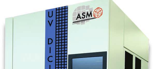
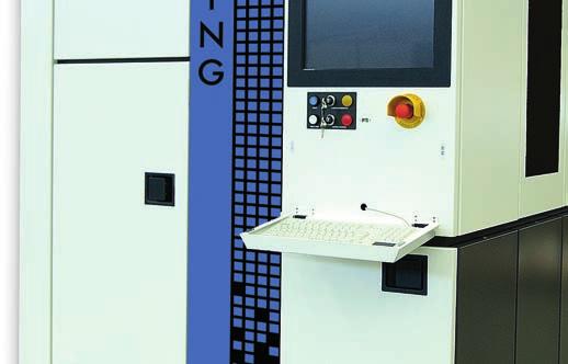
14 Singulation More precision and efficiency: Singulation with the LASER 1205 multi-beam laser system Declining component sizes and wafer thickness, and the desire for more efficiency, i.e. more density on WLP/PLP carriers, require increasingly accurate and gentle component singulation capabilities. Classic saws encounter limitations in terms of cutting width and accuracy when they cut into the carrier (for example, with low-k materials and the resulting threat of contamination) as well at the end of the packaging process. In addition, the packages are subject to mechanical stresses during the sawing process. ASM s LASER 1205 multi-beam laser system is the answer to the rising requirements in singulation. At substrate thicknesses of 100 µm, the cutting width stays below µm with a positioning tolerance of less than < 1 µm. The machine can cut a wide range of materials like silicon wafer (Si, SiC etc.) with thicknesses of up to 250 μm and EMCs with thicknesses of up to 700 µm. Thanks to multi-beam technology, significantly fewer cutting cycles are needed to separate the wafers. As a result, the ASM LASER 1205 achieves exceptionally short cycle times and a correspondingly high level of productivity. LASER 1205 Precise and efficient for silicon and EMC Enabling technology for fan-in applications Precise dicing of molding compound and silicon Higher yield due to minimized dicing street (12-14 µm) No wafer-chipping since the laser cut is aligned precisely within the pre-cut position Seamless transition from fan-in to fan-out with the same basic packaging platform intact 1 2 Deposition Die Attach & SMT 14 Stencil technology Printing

15 3 4 5 Encapsulation Singulation WLP Inspection, Text & Packing 15

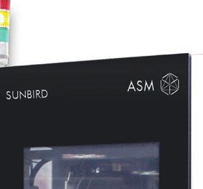
16 WLP Inspection, Test & Packing Finalizing your WLP/PLP processes: SUNBIRD for inspecting, sorting and taping Six-side inspection, electrical tests, laser marking, sorting and taping the SUNBIRD system combines a series of functions in a single machine. And best of all, thanks to the SUNBIRD turret system, it does it all with a high degree of speed and efficiency. In a first step, the machine picks up the packages with its flip arm, inspects their bottom side and passes them to the turret, where they are inspected from six angles, tested, and optionally laser-marked. Thanks to the SUNBIRD s smart iprecise and ialign technologies, the alignment of all components is ensured and optimized via powerful optics and without any additional transfers. Next, the SiP components are gently positioned in tape pockets with automatic Z-axis alignment, under the continuous check of a vision system, which was especially developed for this purpose. That way, even extremely small, thin and sensitive dies can be inspected and taped perfectly. The final sorting step: Divided by software into separate classes, the machine places the components into the tape or different containers. With processing speeds of up to 30,000 UPH, SUNBIRD represents a significant speed and quality improvement over traditional systems. SUNBIRD Extremely efficient inspection, sorting and taping Combines various optical and electrical inspection and (optional) laser marking capabilities in one machine More reliable detection of faults by individual optical inspection Maximum speed of 30,000 UPH thanks to turret system Contactless alignment and smart chip handling ensure optimal package protection Dies are picked directly from the wafer to the turret system and transported through various optical inspection and electrical test positions. Handling of smallest components (0603/0402 metric) 1 2 Deposition Stencil Printing 16 Stencil technology Printing


17 3 4 5 Ball Drop Singulation WLP Inspection, Text & Packing 17
 Market Leadframes ASM Materials")


18 ASM Pacific Technologies Market Assembly & Packaging Equipment ASM Back End Equipment Die & Flip-Chip Bonder Wire Bonder Encapsulation Equipment Tester & Sorter Laser Dicing LED Equipment ASM SMT Solutions SMT Line Solution DEK Printing Solutions SIPLACE Placement Solutions ASM Smart Factory Tools & Services Market SMT Equipment (Printing & Placement) Market Leadframes ASM Materials Leadframes Other Materials Molded Interconnect Substrate (MIS) Invest in a growth market Major trends like digitalization and networking are currently strengthening the interest in advanced packaging technologies worldwide. The underlying idea makes a lot of sense. Instead of combining the components for a module on the circuit board, advanced packaging fi rst integrates dies or fl ip-chips with other SMT components into an SiP, which is then placed on the board. This process allows for further miniaturization, eliminates the time-consuming wire-bonding of dies and frees users from designing required functionalities on their own. The complete function group can be placed as a single module. This convergence of chip assembly and SMT processes opens up new opportunities. Whether semiconductor makers or electronics manufacturers enter this new market either industry requires the other s process knowledge and experience. ASM is your partner of choice ASM is active in both segments. It is the world s only equipment supplier that has been active and successful in both industries chip assembly and SMT. 18


19 ASM PT worldwide With our process, hardware and software specialists, we are a strategic partner of many companies in both industries, and as a technology leader with innovative solutions we keep setting new standards in quality and productivity. This makes ASM your partner of choice for the development, implementation and optimization of consistently integrated and highly automated processes in chip assembly, advanced packaging, and SMT production. We offer end-to-end solution chains and tailor them to the individual requirements and processes of our customers. This brochure presented one example of such a solution chain. If you are interested in putting the opportunities and the potential of advanced packaging to use for your company, get in touch with our experts. By partnering with us you benefi t not only from our extensive product portfolio, but also from our unique process expertise. Your advantage: You do it right the fi rst time while lowering your risks and costs. ASM PT worldwide Present in over 30 countries Over 15,500 employees, including 1,700 in R&D Five Centers of Competence Six R&D centers 10 production locations 1,100 patents in cuttingedge technologies 19
20 ASM Website ASM YouTube ASM Assembly Systems GmbH & Co. KG Rupert-Mayer-Strasse Munich Germany Phone: Fax: Issue 1/ All rights reserved Order No.: A10011-ASM-A103-EN Printed in Germany ASM Assembly Systems GmbH & Co. KG The information in this brochure consists only of general descriptions and/or performance features which may not always apply to concrete products as described or which may change as a result of technical developments or advances. Any specific performance features and/or capabilities will only be binding if contractually agreed upon. All product names are brands or trademarks of ASM Assembly Systems GmbH & Co. KG or other suppliers. Their use by third parties may violate the rights of their owners.
YOUR Strategic TESTING ENGINEERING CONCEPT SMT FLIP CHIP PRODUCTION OPTO PACKAGING PROCESS DEVELOPMENT CHIP ON BOARD SUPPLY CHAIN MANAGEMENT
 YOUR Strategic TECHNOLOGY PARTNER Wafer Back-End OPTO PACKAGING PROCESS DEVELOPMENT CONCEPT FLIP CHIP PROTOTYping ENGINEERING TESTING SMT PRODUCTION CHIP ON BOARD SUPPLY CHAIN MANAGEMENT Next Level 0f
Nanium Overview. Company Presentation
 Nanium Overview Company Presentation Nanium Overview Our name and logo nano prefix of Greek origin referring to small objects ium suffix of Latin origin that includes the formation of scientific terms
MRSI-175Ag Epoxy Dispenser
 MRSI-175Ag Epoxy Dispenser Applications: Microwave & RF Modules MEMS Semiconductor Packaging Multi-Chip Modules Hybrid Circuits Optical Modules Overview The MRSI-175Ag Conductive Epoxy Dispenser handles
Flip Chip - Integrated In A Standard SMT Process
 Flip Chip - Integrated In A Standard SMT Process By Wilhelm Prinz von Hessen, Universal Instruments Corporation, Binghamton, NY This paper reviews the implementation of a flip chip product in a typical
IMPLEMENTATION OF A FULLY MOLDED FAN-OUT PACKAGING TECHNOLOGY
 IMPLEMENTATION OF A FULLY MOLDED FAN-OUT PACKAGING TECHNOLOGY B. Rogers, C. Scanlan, and T. Olson Deca Technologies, Inc. Tempe, AZ USA boyd.rogers@decatechnologies.com ABSTRACT Fan-Out Wafer-Level Packaging
AMERICAS Tel or Tel CHINA, SHENZHEN Tel
 www.uic.com email: universal@uic.com AMERICAS Tel. 1-800-432-2607 or Tel. +1-607-779-7522 CHINA, SHENZHEN Tel. +86-755-2685-9108 CHINA, SHANGHAI Tel. +86-21-6495-2100 EUROPE Tel. +36-23-445-500 2010 Universal
System in Package: Identified Technology Needs from the 2004 inemi Roadmap
 System in Package: Identified Technology Needs from the 2004 inemi Roadmap James Mark Bird Amkor Technology Inc System in package (SiP) technology has grown significantly in the past several years. It
Quality in Electronic Production has a Name: Viscom. System Overview
 Quality in Electronic Production has a Name: Viscom System Overview Successful along the whole line with Viscom Circuit board manufacturing Paste print Finish S3070 AFI-Scan S3054QS Paste print Thick film
System-in-Package (SiP) on Wafer Level, Enabled by Fan-Out WLP (ewlb)
 on Wafer Level, Enabled by Fan-Out WLP (ewlb)") System-in-Package (SiP) on Wafer Level, Enabled by Fan-Out WLP (ewlb) Steffen Kröhnert, José Campos, Eoin O Toole NANIUM S.A., Vila do Conde, Portugal Outline Short Company Overview NANIUM Introduction
System-in-Package (SiP) on Wafer Level, Enabled by Fan-Out WLP (ewlb) Steffen Kröhnert, José Campos, Eoin O Toole NANIUM S.A., Vila do Conde, Portugal Outline Short Company Overview NANIUM Introduction
FLIP CHIP CHIP ON BOARD SMT ENGINEERING OPTO PACKAGING SUPPLY CHAIN MANAGEMENT TESTING YOUR INNOVATIVE TECHNOLOGY PARTNER PRODUCTION CONCEPT
 YOUR INNOVATIVE TECHNOLOGY PARTNER CHIP ON BOARD OPTO PACKAGING PROCESS DEVELOPMENT CONCEPT FLIP CHIP ENGINEERING TESTING PRODUCTION SMT SUPPLY CHAIN MANAGEMENT PROTOTYPES HIGH-PRECISION ASSEMBLY OF MICRO-
TechARENA Packaging Exhibitor Session OCT/08, 2014 New WLP-Technology-Fusion Concept Steffen Kröhnert, Director of Technology, NANIUM S.A. V1.
 TechARENA Packaging Exhibitor Session OCT/08, 2014 New WLP-Technology-Fusion Concept Steffen Kröhnert, Director of Technology, NANIUM S.A. V1.0 EXT Notification NANIUM is highly committed to IP protection.
TSV CHIP STACKING MEETS PRODUCTIVITY
 TSV CHIP STACKING MEETS PRODUCTIVITY EUROPEAN 3D TSV SUMMIT 22-23.1.2013 GRENOBLE HANNES KOSTNER DIRECTOR R&D BESI AUSTRIA OVERVIEW Flip Chip Packaging Evolution The Simple World of C4 New Flip Chip Demands
Chips Face-up Panelization Approach For Fan-out Packaging
 Chips Face-up Panelization Approach For Fan-out Packaging Oct. 15, 2015 B. Rogers, D. Sanchez, C. Bishop, C. Sandstrom, C. Scanlan, TOlson T. REV A Background on FOWLP Fan-Out Wafer Level Packaging o Chips
IME Technical Proposal. High Density FOWLP for Mobile Applications. 22 April High Density FOWLP Consortium Forum
 IME Technical Proposal High Density FOWLP for Mobile Applications 22 April 2014 Packaging driver for portable / mobile applications Key drivers/needs Smaller form-factor lower profile, substrate-less Higher
Basic PCB Level Assembly Process Methodology for 3D Package-on-Package
 Basic PCB Level Assembly Process Methodology for 3D Package-on-Package Vern Solberg STC-Madison Madison, Wisconsin USA Abstract The motivation for developing higher density IC packaging continues to be
Advanced Analytical Techniques for Semiconductor Assembly Materials and Processes. Jason Chou and Sze Pei Lim Indium Corporation
 Advanced Analytical Techniques for Semiconductor Assembly Materials and Processes Jason Chou and Sze Pei Lim Indium Corporation Agenda Company introduction Semiconductor assembly roadmap challenges Fine
QINEO PULSE. The versatile welding machine for industry
 QINEO PULSE The versatile welding machine for industry Some ideas set the trend for future times. PULSE 2 CLOOS: Your brand for innovative welding technology! Providing added value for our customers! This
Smart #1 SMT Factory Our Smart Move to Industry 4.0 Sunil Chhabra, ASM Assembly Systems
 Smart #1 SMT Factory Our Smart Move to Industry 4.0 Sunil Chhabra, ASM Assembly Systems Agenda - Industry 4.0 and the Smart #1 SMT Factory Introduction Industry 4.0 Industry 4.0 vs. Smart Factory Smart
Wire-Bond CABGA A New Near Die Size Packaging Innovation Yeonho Choi February 1, 2017
 Amkor Technology, Inc. White Paper Wire-Bond CABGA A New Near Die Size Packaging Innovation Yeonho Choi February 1, 2017 Abstract Expanding its ChipArray Ball Grid Array (CABGA) package form factor miniaturization
PANTERA Pick + Place. Economical, highly flexible SMD placement system. swiss made
 PANTERA Pick + Place Economical, highly flexible SMD placement system swiss made SMD placement machine for flexible production Feeder capacity 100 x 8 mm Intelligent tape feeder 8 to 56 mm Placement speed
Encapsulation Selection, Characterization and Reliability for Fine Pitch BGA (fpbga )
") Encapsulation Selection, Characterization and Reliability for Fine Pitch BGA (fpbga ) Henry M.W. Sze, Marc Papageorge ASAT Limited 14th Floor, QPL Industrial Building, 138 Texaco Road, Tseun Wan, Hong
Encapsulation Selection, Characterization and Reliability for Fine Pitch BGA (fpbga ) Henry M.W. Sze, Marc Papageorge ASAT Limited 14th Floor, QPL Industrial Building, 138 Texaco Road, Tseun Wan, Hong
SIPLACE X, SIPLACE SX, SIPLACE CA
 SIPLACE Press News Munich, September 16, 2013 ASM Assembly Systems at Productronica 2013 Consistent workflows for electronics production With its presence at the Productronica 2013 trade show (November
Recent Advances in Die Attach Film
 Recent Advances in Die Attach Film Frederick Lo, Maurice Leblon, Richard Amigh, and Kevin Chung. AI Technology, Inc. 70 Washington Road, Princeton Junction, NJ 08550 www.aitechnology.com Abstract: The
Innovative Advanced Wafer Level Packaging with Smart Manufacturing Solutions YOON Seung Wook, Ph.D MBA
 Innovative Advanced Wafer Level Packaging with Smart Manufacturing Solutions YOON Seung Wook, Ph.D MBA Director, STATS ChipPAC Outline 1 2 3 Introduction of Smart Manufacturing & Wafer Level Packaging
KGC SCIENTIFIC Making of a Chip
 KGC SCIENTIFIC www.kgcscientific.com Making of a Chip FROM THE SAND TO THE PACKAGE, A DIAGRAM TO UNDERSTAND HOW CPU IS MADE? Sand CPU CHAIN ANALYSIS OF SEMICONDUCTOR Material for manufacturing process
Chapter 3 Silicon Device Fabrication Technology
 Chapter 3 Silicon Device Fabrication Technology Over 10 15 transistors (or 100,000 for every person in the world) are manufactured every year. VLSI (Very Large Scale Integration) ULSI (Ultra Large Scale
QINEO Product overview
 Product overview Carl Cloos Schweißtechnik GmbH Industriestraße D-35708 Haiger Telefon +49 (0)2773 85-0 Telefax +49 (0)2773 85-275 E-Mail info@cloos.de www.qineo.de CLOOS: Your brand for innovative welding
PDF created with FinePrint pdffactory Pro trial version
 Benefits Damage-free dicing of thin silicon Capable of producing smallest street widths which in return provides additional space for more parts per wafer Single step process results in reduction of cost
Spectrum S-910N Series
 Spectrum S-910N Series Scalable solutions for high-volume dispensing applications Features and Benefits Slim design maximizes floor space utilization and lowers cost of ownership Digital vision system
Automating the In-Circuit Test in Your Factory
 Automating the In-Circuit Test in Your Factory Measurement Test Division Keysight Technologies July 23, 2015 Agenda Page 2 Overview of Inline ICT automation - Introduction to Keysight & In Circuit Test
Failure Modes in Wire bonded and Flip Chip Packages
 Failure Modes in Wire bonded and Flip Chip Packages Mumtaz Y. Bora Peregrine Semiconductor San Diego, Ca. 92121 mbora@psemi.com Abstract The growth of portable and wireless products is driving the miniaturization
Lead-Free Solder Bump Technologies for Flip-Chip Packaging Applications
 Lead-Free Solder Bump Technologies for Flip-Chip Packaging Applications Zaheed S. Karim 1 and Jim Martin 2 1 Advanced Interconnect Technology Ltd. 1901 Sunley Centre, 9 Wing Yin Street, Tsuen Wan, Hong
Novel Materials and Activities for Next Generation Package. Hitachi Chemical., Co.Ltd. Packaging Solution Center Hiroaki Miyajima
 Novel Materials and Activities for Next Generation Package Hitachi Chemical., Co.Ltd. Packaging Solution Center Hiroaki Miyajima 1. Activities of Packaging Solution Center 2. Novel Materials for Next Gen.
Mixed Attachment Technology Studies in RF & Optoelectronic Packages Requiring High Accuracy Placement
 Mixed Attachment Technology Studies in RF & Optoelectronic Packages Requiring High Accuracy Placement Daniel D. Evans and Zeger Bok Palomar Technologies, Inc. 2728 Loker Avenue West Carlsbad, CA 92010
Cost effective 300mm Large Scale ewlb (embedded Wafer Level BGA) Technology
 Technology") Cost effective 300mm Large Scale ewlb (embedded Wafer Level BGA) Technology by Meenakshi Prashant, Seung Wook Yoon, Yaojian LIN and Pandi C. Marimuthu STATS ChipPAC Ltd. 5 Yishun Street 23, Singapore 768442
Cost effective 300mm Large Scale ewlb (embedded Wafer Level BGA) Technology by Meenakshi Prashant, Seung Wook Yoon, Yaojian LIN and Pandi C. Marimuthu STATS ChipPAC Ltd. 5 Yishun Street 23, Singapore 768442
Leveraging the Precision of Electroforming over Alternative Processes When Developing Nano-scale Structures
 VOLUME 4 - ELECTROFORMING Leveraging the Precision of over Alternative Processes When Developing Nano-scale Structures Electrical and mechanical component and subsystem designers generally have five techniques
Challenges for Embedded Device Technologies for Package Level Integration
 Challenges for Embedded Device Technologies for Package Level Integration Kevin Cannon, Steve Riches Tribus-D Ltd Guangbin Dou, Andrew Holmes Imperial College London Embedded Die Technology IMAPS-UK/NMI
Ceramos Gen 5 Details on Handling and Processing Application Note
 Ceramos Gen 5 Details on Handling and Processing Application Note Abstract This application note provides information on handling and processing of the CERAMOS Gen5 (CUW CFUP). CERAMOS Gen5 CUW CFUP The
Glass Carrier for Fan Out Panel Level Package
 January 25, 2018 NEWS RELEASE Development of HRDP TM Material for Formation of Ultra-Fine Circuits with Glass Carrier for Fan Out Panel Level Package - Aiming for mass production in collaboration with
DEK Gemini Platform Technical Specification
 Platform Technical Part No. 573083 Issue 03 August 2014 Machine Standard Configuration Standard Configuration Machine Alignment Capability >2 Cpk @ +/- 12.5µm, 6 Sigma # Process Alignment Capability >2
PRODUCT BROCHURE GLOBAL COORDINATE MEASURING MACHINES
 PRODUCT BROCHURE GLOBAL COORDINATE MEASURING MACHINES 2 GLOBAL Coordinate Measuring Machines TAILORED FOR MAXIMUM PRODUCTIVITY Scalability and scope are the hallmarks of the GLOBAL coordinate measuring
Challenges and Solutions for Cost Effective Next Generation Advanced Packaging. H.P. Wirtz, Ph.D. MiNaPAD Conference, Grenoble April 2012
 Challenges and Solutions for Cost Effective Next Generation Advanced Packaging H.P. Wirtz, Ph.D. MiNaPAD Conference, Grenoble April 2012 Outline Next Generation Package Requirements ewlb (Fan-Out Wafer
Design and Assembly Process Implementation of 3D Components
 IPC-7091 Design and Assembly Process Implementation of 3D Components Developed by the 3-D Electronic Packages Subcommittee (B-11) of the Packaged Electronic Components Committee (B-10) of IPC Users of
3D-WLCSP Package Technology: Processing and Reliability Characterization
 3D-WLCSP Package Technology: Processing and Reliability Characterization, Paul N. Houston, Brian Lewis, Fei Xie, Ph.D., Zhaozhi Li, Ph.D.* ENGENT Inc. * Auburn University ENGENT, Inc. 2012 1 Outline Packaging
Close supply chain collaboration enables easy implementation of chip embedded power SiP
 Close supply chain collaboration enables easy implementation of chip embedded power SiP Gerald Weidinger, R&D Project Leader, AT&S AT & S Austria Technologie & Systemtechnik Aktiengesellschaft Fabriksgasse13
harness manufacturing
 EN harness manufacturing OMEGA 740 750 Komax has developed the fully automatic block loader machines, the Omega 740 and Omega 750, for wire harness production with insertion of housings. The highly flexible
AN Handling and processing of sawn wafers on UV dicing tape. Document information. Sawn wafers, UV dicing tape, handling and processing
 Handling and processing of sawn wafers on UV dicing tape Rev. 2.0 13 January 2009 Application note Document information Info Keywords Abstract Content Sawn wafers, UV dicing tape, handling and processing
SMT Quick-Tips: selecting a custom or used machine. Robert Voigt, DDM Novastar
 SMT Quick-Tips: selecting a custom or used machine Robert Voigt, DDM Novastar When to Consider a Custom or Used Machine Let s say you have an unusual product configuration, a unique space requirement,
Package Solutions and Innovations
 Package Solutions and Innovations with Compression Molding IEEE SVC CPMT Aug 2015 Presented by C.H. Ang Towa USA Company Profile www.cpmt.org/scv 1 Corporate Overview Company: Towa Corp., Kyoto Japan Established:
Multi Rip Saws for Dividing Panel Materials
 Multi Rip Saws for Dividing Panel Materials 02 HOMAG multi rip saws Content HOMAG multi rip saws Content 03 First-Class Saw Quality with HOMAG Machines for Discerning Customers As the degree of automation
Laser Micromachining for Industrial Applications and R&D. 3D-Micromac AG. Symposium on Smart Integrated Systems in Chemnitz. 3D-Micromac AG
 3D-Micromac AG Symposium on Smart Integrated Systems in Chemnitz 1 1 microdice - TLS-Dicing for separation of SiC 2 microprep - for high-throughput microstructure diagnostics 3 About 3D-Micromac AG 2 microdice
Plastics made perfect.
 Plastics made perfect. Plastic injection molding simulation of an electric hedge trimmer. Designed in Inventor software. Simulated in software. Rendered in 3ds Max software. Validation and Optimization
Test Flow for Advanced Packages (2.5D/SLIM/3D)
") 1 Test Flow for Advanced Packages (2.5D/SLIM/3D) Gerard John Amkor Technology Inc. Gerard.John@amkor.com 2045 East Innovation Circle, Tempe, AZ 85284, USA Phone: (480) 821-5000 ADVANCED PACKAGE TEST FLOW
1 Test Flow for Advanced Packages (2.5D/SLIM/3D) Gerard John Amkor Technology Inc. Gerard.John@amkor.com 2045 East Innovation Circle, Tempe, AZ 85284, USA Phone: (480) 821-5000 ADVANCED PACKAGE TEST FLOW
Brochure. Equator gauging systems
 Brochure Equator gauging systems The role of Equator gauging systems on the shop floor To control manufacturing processes, gauges, for example sets of callipers, go / no-go gauges or bore gauges, have
Thin Wafers Bonding & Processing
 Thin Wafers Bonding & Processing A market perspective 2012 Why New Handling Technologies Consumer electronics is today a big driver for smaller, higher performing & lower cost device configurations. These
Spectrum S-920N Series
 Spectrum S-920N Series Scalable solutions for high-volume manufacturing and assembly Features and Benefits The S-920N series leverages over 25 years of Nordson ASYMTEK automated fluid dispensing and jetting
Solutions for handling applications
 Solutions for handling applications Controlled motion sequences faster, simpler and more cost-effective siemens.com/handling Answers for industry. 2 Handling applications efficiently implemented The degree
Spectrum S-920N Series
 Spectrum S-920N Series Scalable solutions for high-volume manufacturing and assembly Features and Benefits The S-920N series leverages over 25 years of Nordson ASYMTEK automated fluid dispensing and jetting
FEATURES OPTIONS FEEDERS
 FEATURES OPTIONS FEEDERS Europlacer s enduring strength lies in its continuing ability to deliver innovative placement solutions without degrading the legendary flexibility that made the company a success.
4 LASER. Laser cutting
 LASER + AUTOMATION 4 LASER Laser cutting Laser cutting is a thermal cutting process for processing sheet metal. The laser beam is created by the laser source (resonator), conducted by a transport fiber
Standard Machines Custom Designs Build-To-Print. Innovative Automation Solutions. Products & Services. Micro Modular System
 Micro Modular System Innovative Automation Solutions MMS was incorporated in 1997. Today, MMS has more than 80 employees working in a modern facility in Penang, Malaysia. Over the years, MMS provided automation
SELECTIVE SOLDERING SYSTEM FLEX400/600
 SELECTIVE SOLDERING SYSTEM FLEX400/600 Fully Automatic Inline System Selective Soldering System FLEX400/600 Wire Soldering Mixed PCB Automotive Sensor Mini SUB Connector Flex PCB to plastic cover Mixed
A new standard in punching efficiency.
 TruPunch: A new standard in punching efficiency. Machine Tools / Power Tools Laser Technology / Electronics Uniquely efficient. Contents Uniquely efficient. 2 Why TruPunch is impressive. 4 Punching tools
Your benefit is our incentive
 MULTIVAC product overview Packaging solutions with method. 2 Your benefit is our incentive MULTIVAC stands for Better Packaging. But what lies behind these two words? As a benefactor of packaging solutions
3D Wirebondless IGBT Module for High Power Applications Dr. Ziyang GAO Jun. 20, 2014
 3D Wirebondless IGBT Module for High Power Applications Dr. Ziyang GAO Jun. 20, 2014 1 1 Outline Background Information Technology Development Trend Technical Challenges ASTRI s Solutions Concluding Remarks
DEK HORIZON ix DL RTC Platform Technical Specification
 DEK HORIZON ix DL RTC Platform Technical Part No. 215449 Issue 05 August 2014 DEK ix DL RTC Machine Standard Configuration Standard Configuration Machine Alignment Capability >2 Cpk @ +/- 12.5µm, 6 Sigma
Company Presentation
 Company Presentation Overview Facts, Vision and Mission Portfolio, Markets and Capabilities Smart Cosmos The Internet of Your Things Quality and Certifications 2 Key Facts Global RFID and IoT pacesetter,
Packaging Commercial CMOS Chips for Lab on a Chip Integration
 Supporting Information for Packaging Commercial CMOS Chips for Lab on a Chip Integration by Timir Datta-Chaudhuri, Pamela Abshire, and Elisabeth Smela Biocompatibility Although the supplier s instructions
SIPLACE SMT-INSIGHTS
 SIPLE SMT-INSIGHTS Progressive oncepts for Modern Electronics Production Editorial SMT production is becoming increasingly complex, especially when the products, which have to be manufactured, are diverse
SMT Quick-Tips: selecting a pick and place machine. Robert Voigt, DDM Novastar
 SMT Quick-Tips: selecting a pick and place machine Robert Voigt, DDM Novastar How To Select A Pick And Place Machine A Pick and Place machine is the second step in a paste, place, reflow assembly operation.
NanoSystemsEngineering: NanoNose Final Status, March 2011
 1 NanoSystemsEngineering: NanoNose Final Status, March 2011 The Nanonose project is based on four research projects (VCSELs, 3D nanolithography, coatings and system integration). Below, the major achievements
BEUMER PALLETISING TECHNOLOGY PRECISE, EFFICIENT, RELIABLE PALLETISING TECHNOLOGY
 PALLETISING TECHNOLOGY PRECISE, EFFICIENT, RELIABLE PALLETISING TECHNOLOGY EFFICIENT AND PRECISE IMPRESSIVE STACK QUALITY For more than 40 years, Group has designed and developed innovative palletising
Microwave Plasma Processing
 Microwave Plasma Processing MUEGGE GMBH Hochstraße 4-6 64385 Reichelsheim Fon +49 (0) 6164-93 07 11 Fax +49 (0) 6164-93 07 93 info@muegge.de www.muegge.de Microwave Plasma Processing Microwave Plasma Technology:
Customizing Processes for Hermetic Assembly Of Devices Designed for Plastic Packages (1 of 3)
") Customizing Processes for Hermetic Assembly Of Devices Designed for Plastic Packages (1 of 3) Charlie C. Megia Golden Altos Corporation 402 South Hillview Drive, Milpitas, CA 95035 cmegia@goldenaltos.com
Customizing Processes for Hermetic Assembly Of Devices Designed for Plastic Packages (1 of 3) Charlie C. Megia Golden Altos Corporation 402 South Hillview Drive, Milpitas, CA 95035 cmegia@goldenaltos.com
Innovative MID Plating Solutions
 Innovative MID Plating Solutions High Reliability Wire Bond Technique for MIDs Jordan Kologe MacDermid Electronics Solutions jkologe@macdermid.com 1 MacDermid: Specialty Chemical Solutions Over 2000 Worldwide
LED Die Attach Selection Considerations
 LED Die Attach Selection Considerations Gyan Dutt & Ravi Bhatkal Alpha, An Alent plc Company Abstract Die attach material plays a key role in performance and reliability of mid, high and super-high power
FOBA Y-Series. High potential fiber marking lasers: More clarity, less complexity. Your product benefits
 FOBA Y-Series High potential fiber marking lasers: More clarity, less complexity Laser marking has become one of the preferred methods for product identification, decoration and material processing. Many
Direct Metal Printers. Metal Additive Manufacturing with the ProX DMP Series
 Direct Metal Printers Metal Additive Manufacturing with the ProX DMP Series Go further with Direct Metal Printing UNLOCK YOUR PRODUCT S POTENTIAL With complete design freedom, direct metal 3D printed parts
Embedding Passive and Active Components: PCB Design and Fabrication Process Variations
 Embedding Passive and Active Components: PCB Design and Fabrication Process Variations Vern Solberg Solberg Technical Consulting Saratoga, California USA Abstract Embedding components within the PC board
SURFACE MOUNT ASSEMBLY OF MINI-CIRCUITS COMPONENTS
 Application Note AN-40-014 SURFACE MOUNT ASSEMBLY OF MINI-CIRCUITS COMPONENTS DATE ISSUED: January 4, 2012 AN-40-014 Rev.: A M150261 (04/14/15) File: AN40014.doc Page 1 of 10 1.0 Introduction Mini-Circuits
2017 Annual Results Announcement. March 1, 2018
 2017 Annual Results Announcement March 1, 2018 Disclaimer The information contained in this presentation is provided for informational purpose only, and should not be relied upon for the purpose of making
Applications of High-Performance MEMS Pressure Sensors Based on Dissolved Wafer Process
 Applications of High-Performance MEMS Pressure Sensors Based on Dissolved Wafer Process Srinivas Tadigadapa and Sonbol Massoud-Ansari Integrated Sensing Systems (ISSYS) Inc., 387 Airport Industrial Drive,
Board Assembly MANUFACTURING TECHNOLOGIES. Wave and Selective Soldering... 48
 Board Assembly Dr. Dongkai Shangguan, Flextronics, Chair Dr. Ravi Bhatkal, Cookson Electronics, Co-Chair David Geiger, Flextronics, Co-Chair CONTENTS: Board Assembly... 1 Executive Summary... 1 Introduction...
CREATING TOMORROW S SOLUTIONS BRIGHT IDEAS. Silicone Solutions for High-Performance LEDs
 CREATING TOMORROW S SOLUTIONS BRIGHT IDEAS Silicone Solutions for High-Performance LEDs LUMISIL SILICONES BRIGHT PERSPECTIVES FOR LED MANUFACTURERS LED lighting brings out the best in silicones they are
Innovative Substrate Technologies in the Era of IoTs
 Innovative Substrate Technologies in the Era of IoTs Dyi- Chung Hu 胡迪群 September 4, 2015 Unimicron Contents Introduction Substrate Technology - Evolution Substrate Technology - Revolution Glass substrate
THE CLUSO VISION SYSTEM AREAS OF APPLICATION
 AREAS OF APPLICATION FIRST ARTICLE INSPECTION Originally designed as a First Article Inspection system, Cluso excels in this space. If human visual inspection is occupying too much time during the line
HYPRES. Hypres MCM Process Design Rules 04/12/2016
 HYPRES Hypres MCM Process Design Rules 04/12/2016 Direct all inquiries, questions, comments and suggestions concerning these design rules and/or HYPRES fabrication to: Daniel T. Yohannes Tel. (914) 592-1190
EMS Electronic Manufacturing Services Excellence in quality and reliability.
 EMS Electronic Manufacturing Services Excellence in quality and reliability www.rafi.de 2 RAFI ELECTRONIC MANUFACTURING SERVICES CUSTOMER BENEFITS WE PROTECT YOUR GOOD REPUTATION RAFI is an owner-managed
"ewlb Technology: Advanced Semiconductor Packaging Solutions"
 "ewlb Technology: Advanced Semiconductor Packaging Solutions" by Sharma Gaurav@, S.W. Yoon, Yap Yok Mian, Shanmugam Karthik, Yaojian Lin, Pandi C. Marimuthu and Yeong J. Lee* STATS ChipPAC Ltd. 5 Yishun
Precision etching of micro components
 Precision etching of micro components A High-Tech Profile Micrometal manufactures customized, highly accurate etched components. We photochemically etch these parts from thin materials (starting at 0.025
Agilent Transducer Systems
 Agilent Transducer Systems Leading the Future for Extreme Accuracy Positioning Applications Highest accuracy Flexible standard system design Custom design available Agilent Laser Interferometry Systems
FLX2011-MKL Pick&Place
 FLX2011-MKL Pick&Place Assembly system for flexible printed circuits and membrane keyboards Glue and paste dispensing SMD and LED placement swiss made Metal dome placement Assembly system for flexible
Rockwell R RF to IF Down Converter
 Construction Analysis Rockwell R6732-13 RF to IF Down Converter Report Number: SCA 9709-552 Global Semiconductor Industry the Serving Since 1964 17350 N. Hartford Drive Scottsdale, AZ 85255 Phone: 602-515-9780
Coil on Module. Packaging innovation for egov documents.
 Coil on Module Packaging innovation for egov documents www.infineon.com/com Abstract Modern ID cards are required to stand up to many types of stress, ranging from attempts at physical alteration, to wear
31. CUSTOM DEVICE CONNECTIVITY
 . CUSTOM DEVICE CONNECTIVITY Individual device connectivity tailored to device versatility. When customized products are called for, you can always rely on HARTING. HARTING offers a wide range of series
Analog Devices ADSP KS-160 SHARC Digital Signal Processor
 Construction Analysis Analog Devices ADSP-21062-KS-160 SHARC Digital Signal Processor Report Number: SCA 9712-575 Global Semiconductor Industry the Serving Since 1964 17350 N. Hartford Drive Scottsdale,
Plastic Electronics Precise and productive automation solutions
 Plastic Electronics Precise and productive automation solutions 2 Plastic Electronics Flexible electronics "off the roll" Today s electronics industry faces constant challenges as resource and energy costs
Semiconductor IC Packaging Technology Challenges: The Next Five Years
 SPAY025 May 2006 White Paper Mario A. Bolanos, Director Semiconductor Group Packaging Technology Development, Texas Instruments In the era of communications and entertainment, growth of consumer electronics
Selection and Application of Board Level Underfill Materials
 Selection and Application of Board Level Underfill Materials Developed by the Underfill Materials Design, Selection and Process Task Group (5-24f) of the Assembly and Joining Committee (5-20) of IPC Supersedes: