BPS Surfactant-Formulated, Multifunction Dicing Solutions
|
|
|
- Laurel Terry
- 6 years ago
- Views:
Transcription


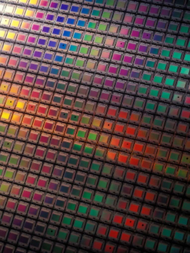
1 BPS Surfactant-Formulated, Multifunction Dicing Solutions Lowering costs of ownership, improving yields A major breakthrough for silicon, BGA, and ceramics dicing applications.
 chemistries effectively remove saw residues (swarf) through better wetting, while removing and mitigating the regrowth of metal oxides from bond pads and")
 Residue Removal Sufactant Low Foam High Conductivity High Product Dilution Does Not")

2 Dice with BPS! For dicing, BPS (Better Process Solutions) chemistries effectively remove saw residues (swarf) through better wetting, while removing and mitigating the regrowth of metal oxides from bond pads and bumps. Fig. 1: The BPS Value Proposition for Dicing CO 2 BPS-729 BPS-729-B Comps Basic Product Cut Quality (Heat Dissipation) Residue Removal Sufactant Low Foam High Conductivity High Product Dilution Does Not Support Bio-Growth Dioxin/Silicone/Mineral Oil-Free Long Shelf-Life N/A N/A N/A Premium Product Cu Ox Removal Cu Ox Regrowth Reduction Al Ox Removal w/bps-100 Gain improved technical performance at the same cost using Air Products BPS products. An Overview Air Products BPS (Better Process Solutions) products are aqueous solutions that are made for cleaning applications in electronics test, assembly, and packaging specifically to improve yields at probe/ test, as a dicing solution, allowing flux-less bump reflow and reducing no-sticks at wirebond all on a variety of substrates. BPS solutions have extremely low etch rates on commonly used substrates in the industry, selectively removing metal oxides, fluorine, organic residues, and particulate contaminants. Air Products has developed the right solutions for your wafer manufacturing needs. We have a broad portfolio of materials, the technical expertise needed to help you integrate them quickly into your processes, and the focus to provide these solutions effectively. BPS products can be safely used on a variety of devices including PCBs, WLCSP, CSP, MEMS, and flip-chips to remove oxides from Al and Cu pads as well as Sn/Pb and Pb-free solder bumps while causing no damage to base metals and substrates such as Si, GaAs, InP, and passivation layers. Fig. 2: Clean Up Your Bond Pads Our Advanced Dicing Solutions The BPS-729 series products are surfactant-containing aqueous solutions that are injected into the DIW stream as you dice. Featuring low-foam, high conductivity, and a two-year shelf life, BPS-729 series products can help eliminate the need for CO 2 sparging. Depending on your application, BPS-729 series products can work at dilutions as low as 1000:1 in DIW, reflecting in a lowered cost of ownership. The BPS-729 series reduces kerf, chipping, and burring on various substrates including silicon, ceramics and BGA, with proven stability in closed-loop recirculation systems. BPS products contain no PFOS, mineral oils, silicones, or dioxins, and are compatible with commonly used blades and materials of construction. BPS-729-B is our super-low-resistivity dicing solution that is especially suitable for static-sensitive devices. Electrostatic discharge (ESD) can damage vital components on your product and also increase the accumulation of residues as you dice. BPS-729-B reduces the resistivity of your dicing solution by orders of magnitude! BPS- 729-B lowers surface tension substantially even at 1000:1, allowing more cooling water to enter deep cuts, cool the blade, and effectively carry away swarf. Recommended for use at dilutions between 200:1 and 1000:1. Remove and prevent corrosion, and Increase conductivity of bond pads. Saw using DIW. Saw using BPS Air Products: BPS Surfactant-Formulated, Multifunction Dicing Solutions
3


: Copper* Dice using DIW Leaves thick residue/swarf. Wafer had to be scrubbed (on left) to remove swarf. Dice using BPS-729 @ 1000:1 Cleans wafer completely!")


4 BPS-729 is our premium dicing solution that not only prevents adherence of silicon particles and saw residue (swarf), but also removes oxidation from bond pads or bumps and retards their regrowth. Because of a very low etch rate on various materials, base metals are not affected. BPS-729 works through a combination of surfactant action and a unique micro under-etch process that dislodges particles embedded in the surface without affecting the underlying substrate. BPS-729 is specially engineered for ultra-low foam to prolong the life of your equipment. BPS-729 is recommended for use between 200:1 to 1000:1 in DIW dilutions for most cleaning applications; ~100:1 for copper oxide removal; and ~100:1 for aluminum oxide removal in combination with a pretreatment of BPS-100. Air Products has a broad portfolio of materials to help customers improve their wafer manufacturing processes. BPS Solutions Work These actual comparisons underscore the effectiveness of Air Products BPS-729 for dicing: Fig. 3: Cleaning (Swarf Removal): Aluminum* Fig. 4: Cleaning (Swarf Removal): Copper* Dice using DIW Leaves thick residue/swarf. Wafer had to be scrubbed (on left) to remove swarf. Dice using 1000:1 Cleans wafer completely! No need for scrubbing wafer! Dice using DIW Leaves thick residue/swarf. Wafer had to be scrubbed (on left) to remove swarf. Dice using 1000:1 Cleans wafer completely! No need for scrubbing wafer! BPS solutions effectively removed swarf through superior wetting even down to 1000:1 dilution eliminating additional rinse processes. Fig. 5: High Conductivity Applications Fig. 6: Foaming Performance Chemistry (w/lab-quality DIW) DIW DIW + CO 2 500:1 500:1 Resistivity (M-Ohm) <0.05 < BPS-729 and BPS-729-B reduce resistivity of DIW more effectively than carbon dioxide can by several orders of magnitude allowing you to dice static-sensitive devices. BPS-729 Competitor Surfactant 100:1 1000:1 100:1 1000:1 BPS-729 is engineered for ultra-low foam performance! At 1000:1 dilutions, foam created by BPS-729 disappears in under 3 minutes (left) versus 15 minutes for a competitive surfactant. The BPS Product Family BPS wet chemistries are an efficient and simple way of removing metal oxides, fluorine, particulate contamination, organic residues and flux from wafers without damaging the underlying metals. Customers benefit from lower costs through improved yield and lowered reruns in their test, assembly, and packaging applications. * LoadPoint NanoAce tool; 6 SI wafer with 25mm x 25mm cut; 4 minute saw process; scrub LHS; dry spin; inspected in black box environment. 3. Three distinct product groupings include photo resist and flux removers (BPS-125), oxide removers (BPS-170, BPS-172, BPS-100 and BPS-101), and dicing solutions (BPS-729 and BPS-729-B) all designed to eliminate or minimize problems caused by residues and metal oxides. BPS solutions in cleaning applications have short processing times and a much lower cost associated with them than current techniques.


5 BPS Dicing Solutions: The RIght Stuff The BPS-729 series of products for dicing... Remove saw residues using advanced surfactant technology to effectively reduce surface tension to prevent embedding of surface particles. Improve kerf and chipping performance on silicon, BGA, and ceramics. Lower resistivity to reduce ESD. Lower foam compared to conventional surfactants. Exhibit stable performance in closed-loop recirculation systems. Further lower cost-of-ownership with dilutions as low as 1000:1 in DIW. Prevent bond pad corrosion and mitigate oxide regrowth (BPS-729). Do not attack base metals. Typical etch rates on commonly used metals are < 1A/min. Remove copper oxides as you dice to improve downstream wire bonding processes; mitigates regrowth for up to 14 days! Remove Al oxides in combination with BPS-100. Do not attack dicing blades. Accommodate most existing tools without retrofits. Do not sustain bacteria and other bio-growth. Do not contain PFOS, mineral oils, silicones or dioxins Have a two-year shelf life and do not separate or coagulate over time. Are compatible with commonly used materials of constructions. BPS solutions save you more because they have a two-year shelf life, can be applied at room temperature, and do not contain PFOS or silicones. We ve packaged them they way you need them gallon bottles, five-gallon pails, 55-gallon drums, or 200-gallon totes. The Power of BPS in Oxide Removal Cleaner, oxide/corrosion-free bond pads and bumps mean improved performance through lower failure rates at downstream operations such as wire bonding, flip-chip bonding, reflow and soldering! BPS-729 is our premium product that removes metal oxides off bond pads and bumps as you dice, improving their conductivity while causing no damage to the underlayers and vital components. Gentle on metals, tough on oxides! BPS-729 provides additional cost of ownership benefits by removing the need for costly plasma etch processes. BPS solutions save you more because they have a two-year shelf life, can be applied at room temperature, and do not contain PFOS or silicones. We ve packaged them they way you need them gallon bottles, five-gallon pails, 55-gallon drums or 200-gallon totes. Fig. 7: Aluminum Oxide Removal* (Bond Pads) Fig. 8: Copper Oxide Removal: BPS-729 Initial Thickness Final Thickness Dice using DIW. Dice using BPS-729 after BPS-100 pre-treatment. BPS-729 in combination with a pre-treatment of BPS-100 allows you to remove aluminum oxide that makes your bond pads like new! Note the clarity of the grain boundaries after treatment. * LoadPoint NanoAce tool; 6 SI wafer with 25mm x 25mm cut; 4-min. sawing; scrub LHS; dry spin; black box inspect. Cu Ox Thickness in A BPS-729 removes copper oxide effectively even down to 100:1 dilution Before After Oxide Re-growth Before Total Oxide Removal After DIW 125:1

6 Our Emphasis on Safety We are an electronics materials supplier customers know and trust. We work to fully understand our customers needs and to help them find the best materials solutions. But, most importantly, the people on our Electronics Division team are passionate about what they do. They are determined to help every customer squeeze the most out of every molecule, and to deliver those molecules 24/7 to where they re needed, when they re needed. A H i s t o r y o f P r o v e n P e r f o r m a n c e & Commitment to Our Customers This brochure provides only a brief overview of our broad range of capabilities for improving testing, packaging, and assembly applications. We are involved in all aspects of wafer cleaning. We have nearly four decades of electronics industry experience and local expertise. We will help you develop the smaller, faster and more powerful electronics the world demands. Visit us at or contact: For More Information Corporate Headquarters Air Products and Chemicals 7201 Hamilton Boulevard Allentown, PA Tel Tel Fax Fax Air Products Asia, Inc. Electronics Division Headquarters 2F, No. 21, Section 2 Chung Shang North Road Taipei 104, Taiwan Tel Fax Europe Headquarters Air Products PLC Hersham Place Technology Park Molesey Road, Hersham Walton-on-Thames Surrey KT12 4RZ, UK Tel Fax Giorgio Technology Sales/Service Mesa, AZ gtsaz@aol.com Optimizing the cost-of-ownership for customers is our focus. tell me more Air Products and Chemicals, Inc., GLB-Oct09
Fluxless soldering using Electron Attachment (EA) Technology
 Technology") Fluxless soldering using Electron Attachment (EA) Technology Proprietary, patented innovation for wafer level packaging applications including wafer bump and copper pillar reflow. Air Products has partnered
Fluxless soldering using Electron Attachment (EA) Technology Proprietary, patented innovation for wafer level packaging applications including wafer bump and copper pillar reflow. Air Products has partnered
Production-scale Flux-free Bump Reflow Using Electron Attachment
 Production-scale Flux-free Bump Reflow Using Electron Attachment C. Christine Dong, Richard E. Patrick, Gregory K. Arslanian, Tim Bao Kail Wathne, and Phillip Skeen Air Products and Chemicals, Inc., Allentown,
Atmosphere Effect on Soldering of Flip Chip Assemblies. C. C. Dong Air Products and Chemicals, Inc. U.S.A.
 Atmosphere Effect on Soldering of Flip Chip Assemblies C. C. Dong Air Products and Chemicals, Inc. U.S.A. Atmosphere Effect on Soldering of Flip Chip Assemblies Abstract An experimental study was conducted
SEMICONDUCTOR WAFER-DIE SEPARATION SOLUTIONS
 UDM Systems, LLC SEMICONDUCTOR WAFER-DIE SEPARATION SOLUTIONS Advantages of UDM Systems Semiconductor Products UDM Systems, LLC products are specifically designed for use in multiple applications in semiconductor
Microwave Plasma Processing
 Microwave Plasma Processing MUEGGE GMBH Hochstraße 4-6 64385 Reichelsheim Fon +49 (0) 6164-93 07 11 Fax +49 (0) 6164-93 07 93 info@muegge.de www.muegge.de Microwave Plasma Processing Microwave Plasma Technology:
Lattice isplsi1032e CPLD
 Construction Analysis Lattice isplsi1032e CPLD Report Number: SCA 9612-522 Global Semiconductor Industry the Serving Since 1964 15022 N. 75th Street Scottsdale, AZ 85260-2476 Phone: 602-998-9780 Fax: 602-948-1925
Rockwell R RF to IF Down Converter
 Construction Analysis Rockwell R6732-13 RF to IF Down Converter Report Number: SCA 9709-552 Global Semiconductor Industry the Serving Since 1964 17350 N. Hartford Drive Scottsdale, AZ 85255 Phone: 602-515-9780
IPC-AJ-820A Assembly and Joining Handbook. The How and Why of All Things PCB & PCA
 IPC-AJ-820A Assembly and Joining Handbook The How and Why of All Things PCB & PCA 1 Scope To provide guidelines and supporting info for the mfg of electronic equipment To explain the HOW TO and WHY Discussions
LED Die Attach Selection Considerations
 LED Die Attach Selection Considerations Gyan Dutt & Ravi Bhatkal Alpha, An Alent plc Company Abstract Die attach material plays a key role in performance and reliability of mid, high and super-high power
3D-WLCSP Package Technology: Processing and Reliability Characterization
 3D-WLCSP Package Technology: Processing and Reliability Characterization, Paul N. Houston, Brian Lewis, Fei Xie, Ph.D., Zhaozhi Li, Ph.D.* ENGENT Inc. * Auburn University ENGENT, Inc. 2012 1 Outline Packaging
Advanced Analytical Techniques for Semiconductor Assembly Materials and Processes. Jason Chou and Sze Pei Lim Indium Corporation
 Advanced Analytical Techniques for Semiconductor Assembly Materials and Processes Jason Chou and Sze Pei Lim Indium Corporation Agenda Company introduction Semiconductor assembly roadmap challenges Fine
WF6317. A superactive low-volatile/high heat-resistant water-soluble flux for ball soldering
 WF637 A superactive low-volatile/high heat-resistant water-soluble flux for ball soldering Low viscosity and high tacking power stabilize ball holding force and ensures excellent solder wettability Easy
Ultra Fine Pitch Bumping Using e-ni/au and Sn Lift-Off Processes
 Ultra Fine Pitch Bumping Using e-ni/au and Sn Lift-Off Processes Andrew Strandjord, Thorsten Teutsch, and Jing Li Pac Tech USA Packaging Technologies, Inc. Santa Clara, CA USA 95050 Thomas Oppert, and
YOUR Strategic TESTING ENGINEERING CONCEPT SMT FLIP CHIP PRODUCTION OPTO PACKAGING PROCESS DEVELOPMENT CHIP ON BOARD SUPPLY CHAIN MANAGEMENT
 YOUR Strategic TECHNOLOGY PARTNER Wafer Back-End OPTO PACKAGING PROCESS DEVELOPMENT CONCEPT FLIP CHIP PROTOTYping ENGINEERING TESTING SMT PRODUCTION CHIP ON BOARD SUPPLY CHAIN MANAGEMENT Next Level 0f
Challenges and Solutions for Cost Effective Next Generation Advanced Packaging. H.P. Wirtz, Ph.D. MiNaPAD Conference, Grenoble April 2012
 Challenges and Solutions for Cost Effective Next Generation Advanced Packaging H.P. Wirtz, Ph.D. MiNaPAD Conference, Grenoble April 2012 Outline Next Generation Package Requirements ewlb (Fan-Out Wafer
Close supply chain collaboration enables easy implementation of chip embedded power SiP
 Close supply chain collaboration enables easy implementation of chip embedded power SiP Gerald Weidinger, R&D Project Leader, AT&S AT & S Austria Technologie & Systemtechnik Aktiengesellschaft Fabriksgasse13
PerformanceProfile. Initial Tests Demonstrate Improved Yield. Introduction
 PerformanceProfile Replacing Hydroxyl-amine-based Chemistries with Semi-aqueous-based Cleaning Formulations Generates Improved Yields in Post-etch Metal and Oxide Residue Removal by: Mustapha, Nik Senior
Dallas Semicoductor DS80C320 Microcontroller
 Construction Analysis Dallas Semicoductor DS80C320 Microcontroller Report Number: SCA 9702-525 Global Semiconductor Industry the Serving Since 1964 15022 N. 75th Street Scottsdale, AZ 85260-2476 Phone:
IMPLEMENTATION OF A FULLY MOLDED FAN-OUT PACKAGING TECHNOLOGY
 IMPLEMENTATION OF A FULLY MOLDED FAN-OUT PACKAGING TECHNOLOGY B. Rogers, C. Scanlan, and T. Olson Deca Technologies, Inc. Tempe, AZ USA boyd.rogers@decatechnologies.com ABSTRACT Fan-Out Wafer-Level Packaging
Silicon Wafer Processing PAKAGING AND TEST
 Silicon Wafer Processing PAKAGING AND TEST Parametrical test using test structures regularly distributed in the wafer Wafer die test marking defective dies dies separation die fixing (not marked as defective)
Engineered Media for Municipal and Industrial Applications
 Engineered Media for Municipal and Industrial Applications A Higher Level of Filtration Performance PERF Fairmount Water Solutions Is Raising the Bar on Filtration Media Performance Fairmount Water Solutions
Lead Free Surface Mount Technology. Ian Wilding BSc Senior Applications Engineer Henkel Technologies
 Lead Free Surface Mount Technology Ian Wilding BSc Senior Applications Engineer Henkel Technologies Overview of the Presentation First contact: Impact on the production operator Packaging Labelling Impact
UTILIZATION OF ATMOSPHERIC PLASMA SURFACE PREPARATION TO IMPROVE COPPER PLATING PROCESSES.
 SESSION 14 MATERIALS AND PROCESSES FOR ADVANCED PACKAGING UTILIZATION OF ATMOSPHERIC PLASMA SURFACE PREPARATION TO IMPROVE COPPER PLATING PROCESSES. Eric Schulte 1, Gilbert Lecarpentier 2 SETNA Corporation
Enabling Low Defectivity Solutions Through Co- Development of CMP Slurries and Cleaning Solutions for Cobalt Interconnect Applications
 Enabling Low Defectivity Solutions Through Co- Development of CMP Slurries and Cleaning Solutions for Cobalt Interconnect Applications Dnyanesh Tamboli 1, Tom Shi 1, Chris Li 2, Ming-Shih Tsai 2, Rung-Je
THIN IMMERSION TIN USING ORGANIC METALS
 THIN IMMERSION TIN USING ORGANIC METALS Jim Kenny, Nils Arendt, Bernhard Wessling, and Karl Wengenroth Enthone Inc., A Business of Cookson Electronics West Haven, CT, USA ABSTRACT With the international
Failure Modes in Wire bonded and Flip Chip Packages
 Failure Modes in Wire bonded and Flip Chip Packages Mumtaz Y. Bora Peregrine Semiconductor San Diego, Ca. 92121 mbora@psemi.com Abstract The growth of portable and wireless products is driving the miniaturization
Chapter 3 Silicon Device Fabrication Technology
 Chapter 3 Silicon Device Fabrication Technology Over 10 15 transistors (or 100,000 for every person in the world) are manufactured every year. VLSI (Very Large Scale Integration) ULSI (Ultra Large Scale
Interfacial Reactions between the Sn-9Zn Solder and Au/Ni/SUS304 Multi-layer Substrate
 , July 6-8, 2011, London, U.K. Interfacial Reactions between the Sn-9Zn Solder and Au/Ni/SUS304 Multi-layer Substrate *Yee-Wen Yen 1, Chien-Chung Jao 2, Kuo-Sing Chao 1, Shu-Mei Fu Abstract Sn-9Zn lead-free
ELECTRONIC GRADE SULFAMATE NICKEL Document ID: EFM1409
 ELECTRONIC GRADE SULFAMATE NICKEL Document ID: EFM1409 E-Form is an electronic grade nickel sulfamate electroforming concentrate designed and manufactured specifically for use with microlithography. DisChem
Analog Devices ADSP KS-160 SHARC Digital Signal Processor
 Construction Analysis Analog Devices ADSP-21062-KS-160 SHARC Digital Signal Processor Report Number: SCA 9712-575 Global Semiconductor Industry the Serving Since 1964 17350 N. Hartford Drive Scottsdale,
Bridging Supply Chain Gap for Exempt High-Reliability OEM s
 Bridging Supply Chain Gap for Exempt High-Reliability OEM s Hal Rotchadl hrotchadl@premiers2.com www.premiers2.com Premier Semiconductor Services Tempe, AZ RoHS exempt high reliability OEMs breathed a
Abstract. Introduction
 Accelerating Silicon Carbide Power Electronics Devices into High Volume Manufacturing with Mechanical Dicing System By Meng Lee, Director, Product Marketing and Jojo Daof, Senior Process Engineer Abstract
Compounds. Table of Contents. or TABLE OF CONTENTS
 Table of Contents Compounds TABLE OF CONTENTS Compounds Pictorial Index... 470 HiTemp Universal Compound (HiTUC)... 471 AFL No. 2 Electrical Joint Compound... 472 Alnox Electrical Joint Compound... 473
3D Wirebondless IGBT Module for High Power Applications Dr. Ziyang GAO Jun. 20, 2014
 3D Wirebondless IGBT Module for High Power Applications Dr. Ziyang GAO Jun. 20, 2014 1 1 Outline Background Information Technology Development Trend Technical Challenges ASTRI s Solutions Concluding Remarks
National Semiconductor LM2672 Simple Switcher Voltage Regulator
 Construction Analysis National Semiconductor LM2672 Simple Switcher Voltage Regulator Report Number: SCA 9712-570 Global Semiconductor Industry the Serving Since 1964 17350 N. Hartford Drive Scottsdale,
QUALITEK 302+ NO CLEAN FLUX
 QUALITEK 32+ NO CLEAN FLUX CORPORATE HEADQUARTERS USA: 315 Fairbank St. Addison, IL 63-628-883 FAX 63-628-6543 EUROPE UK: Unit 9 Apex Ct. Bassendale Rd. Bromborough, Wirral CH62 3RE 44 151 334 888 FAX
Nickel-bond Blades The best choice for soft material and machinable hard material applications
 Nickel-bond Blades The best choice for soft material and machinable hard material applications A Comprehensive Dicing Solution The hardest binder for superior wear resistance The thinnest blade available
Author: Anthony Jones Presented by: Sarah Gibson
 Unique Industrial Hygiene Aspects in Gallium Arsenide Device Manufacturing Facilities Author: Anthony Jones Presented by: Sarah Gibson Outline Gallium arsenide overview Various operations IH issues MOCVD
RF System in Packages using Integrated Passive Devices
 RF System in Packages using Integrated Passive Devices by Kai Liu, YongTaek Lee, HyunTai Kim, Gwang Kim, and Billy Ahn STATS ChipPAC 1711 W. Greentree Drive, Suite #117, Tempe, AZ 85284, USA Tel: 480-222-1722
EPOXY FLUX MATERIAL AND PROCESS FOR ENHANCING ELECTRICAL INTERCONNECTIONS
 As originally published in the SMTA Proceedings. EPOXY FLUX MATERIAL AND PROCESS FOR ENHANCING ELECTRICAL INTERCONNECTIONS Neil Poole, Ph.D., Elvira Vasquez, and Brian J. Toleno, Ph.D. Henkel Electronic
HYPRES. Hypres MCM Process Design Rules 04/12/2016
 HYPRES Hypres MCM Process Design Rules 04/12/2016 Direct all inquiries, questions, comments and suggestions concerning these design rules and/or HYPRES fabrication to: Daniel T. Yohannes Tel. (914) 592-1190
Case Study Power Electronics Cleaning - Solvent to ph Neutral: Enhancing Safety, Process Efficiency and Productivity
 Case Study Power Electronics Cleaning - Solvent to ph Neutral: Enhancing Safety, Process Efficiency and Productivity Ravi Parthasarathy, M.S.Ch.E. Senior Application Engineer ZESTRON Americas Outline Introduction
1 Thin-film applications to microelectronic technology
 1 Thin-film applications to microelectronic technology 1.1 Introduction Layered thin-film structures are used in microelectronic, opto-electronic, flat panel display, and electronic packaging technologies.
N/C No Charge ( Static Dissipative Floor Finish
 !"# $ %&%"'# %"'#()')*$')+,""#,% $%-./.01! N/C No Charge ( Static Dissipative Floor Finish Static contamination you cannot feel it at levels under 3,500 volts Static contamination you cannot see it at
Ingot/Boule - Wafering & Slicing Precision Surface Cleaning Solutions for Photovoltaic Wafers. Advantages of UDM Systems Solar (PV) Products
 Products") Ingot/Boule - Wafering & Slicing Precision Surface Cleaning Solutions for Photovoltaic Wafers UDM Systems, LLC Advantages of UDM Systems Solar (PV) Products UDM Systems has revolutionized the solar industry
Ingot/Boule - Wafering & Slicing Precision Surface Cleaning Solutions for Photovoltaic Wafers UDM Systems, LLC Advantages of UDM Systems Solar (PV) Products UDM Systems has revolutionized the solar industry
HBLED packaging is becoming one of the new, high
 Ag plating in HBLED packaging improves reflectivity and lowers costs JONATHAN HARRIS, President, CMC Laboratories, Inc., Tempe, AZ Various types of Ag plating technology along with the advantages and limitations
Plasma for Underfill Process in Flip Chip Packaging
 Plasma for Underfill Process in Flip Chip Packaging Jack Zhao and James D. Getty Nordson MARCH 2470-A Bates Avenue Concord, California 94520-1294 USA Published by Nordson MARCH www.nordsonmarch.com 2015
Intel Pentium Processor W/MMX
 Construction Analysis Intel Pentium Processor W/MMX Report Number: SCA 9706-540 Global Semiconductor Industry the Serving Since 1964 15022 N. 75th Street Scottsdale, AZ 85260-2476 Phone: 602-998-9780 Fax:
LGIT CSP Application NOTE. (Lighting)
") LGIT CSP Application NOTE (Lighting) TABLE OF CONTENTS 1. LGIT CSP Detail -------------- P2 2. LGIT CSP PCB Design -------------- P3 2.1. LGIT CSP Footprint and PCB Pattern -------------- P3 2.2. PCB Substrate
LGIT CSP Application NOTE (Lighting) TABLE OF CONTENTS 1. LGIT CSP Detail -------------- P2 2. LGIT CSP PCB Design -------------- P3 2.1. LGIT CSP Footprint and PCB Pattern -------------- P3 2.2. PCB Substrate
Low Cost Flip Chip Bumping
 Low Cost Flip Bumping Thomas Oppert, Thorsten Teutsch, Elke Zakel Pac Tech Packaging Technologies GmbH Am Schlangenhorst 15 17 D-14641 Nauen, Germany Phone: +49 (0)3321/4495 0 Fax: +49 (0)3321/4495 23
Guidelines for Vishay Sfernice Resistive and Inductive Components
 VISHAY SFERNICE www.vishay.com Resistive and Inductive Products By Pascale Nagy Caution: Information included in product datasheets are ing to the general information given in this 1. STORAGE RECOMMENDATION
FLIP CHIP CHIP ON BOARD SMT ENGINEERING OPTO PACKAGING SUPPLY CHAIN MANAGEMENT TESTING YOUR INNOVATIVE TECHNOLOGY PARTNER PRODUCTION CONCEPT
 YOUR INNOVATIVE TECHNOLOGY PARTNER CHIP ON BOARD OPTO PACKAGING PROCESS DEVELOPMENT CONCEPT FLIP CHIP ENGINEERING TESTING PRODUCTION SMT SUPPLY CHAIN MANAGEMENT PROTOTYPES HIGH-PRECISION ASSEMBLY OF MICRO-
Embedding Passive and Active Components: PCB Design and Fabrication Process Variations
 Embedding Passive and Active Components: PCB Design and Fabrication Process Variations Vern Solberg Solberg Technical Consulting Saratoga, California USA Abstract Embedding components within the PC board
TSV Processing and Wafer Stacking. Kathy Cook and Maggie Zoberbier, 3D Business Development
 TSV Processing and Wafer Stacking Kathy Cook and Maggie Zoberbier, 3D Business Development Outline Why 3D Integration? TSV Process Variations Lithography Process Results Stacking Technology Wafer Bonding
KGC SCIENTIFIC Making of a Chip
 KGC SCIENTIFIC www.kgcscientific.com Making of a Chip FROM THE SAND TO THE PACKAGE, A DIAGRAM TO UNDERSTAND HOW CPU IS MADE? Sand CPU CHAIN ANALYSIS OF SEMICONDUCTOR Material for manufacturing process
Ultra thin chips for miniaturized products
 Ultra thin chips for miniaturized products Authors: Erik Jung, A. Ostmann (*),D. Wojakowski, C. Landesberger ( + ), R. Aschenbrenner, H. Reichl (*) FhG-IZM, TU Berlin (*) Gustav-Meyer-Allee 25, Berlin
Cree EZ-p LED Chips Handling and Packaging Recommendations
 Cree EZ-p LED Chips Handling and Packaging Recommendations INTRODUCTION This application note provides the user with an understanding of Cree s EZ-p p-pad up (anode up) LED devices, as well as recommendations
Chips Face-up Panelization Approach For Fan-out Packaging
 Chips Face-up Panelization Approach For Fan-out Packaging Oct. 15, 2015 B. Rogers, D. Sanchez, C. Bishop, C. Sandstrom, C. Scanlan, TOlson T. REV A Background on FOWLP Fan-Out Wafer Level Packaging o Chips
Chemraz (FFKM) Overview
 Overview") (FFKM) Overview 505 Energy Midstream Coupling Broad chemical compatibility for use with a wide range of harsh solutions Lower compression set increases ability to handle temp and pressure variations, shaft
(FFKM) Overview 505 Energy Midstream Coupling Broad chemical compatibility for use with a wide range of harsh solutions Lower compression set increases ability to handle temp and pressure variations, shaft
Custom Pack and Air Products Our work together
 Custom Pack and Air Products Our work together We develop solutions together with our customers to help them run their operations more efficiently. It s about teamwork. Danna LeBlanc, Air Products Account
"ewlb Technology: Advanced Semiconductor Packaging Solutions"
 "ewlb Technology: Advanced Semiconductor Packaging Solutions" by Sharma Gaurav@, S.W. Yoon, Yap Yok Mian, Shanmugam Karthik, Yaojian Lin, Pandi C. Marimuthu and Yeong J. Lee* STATS ChipPAC Ltd. 5 Yishun
Packaging Commercial CMOS Chips for Lab on a Chip Integration
 Supporting Information for Packaging Commercial CMOS Chips for Lab on a Chip Integration by Timir Datta-Chaudhuri, Pamela Abshire, and Elisabeth Smela Biocompatibility Although the supplier s instructions
Quality and Reliability Report
 Quality and Reliability Report Product Qualification MASW-007921 2mm 8-Lead Plastic Package QTR-0148 M/A-COM Technology Solutions Inc. 100 Chelmsford Street Lowell, MA 01851 Tel: (978) 656-2500 Fax: (978)
Manufacturing Process
 Digital Integrated Circuits A Design Perspective Jan M. Rabaey Anantha Chandrakasan Borivoje Nikolic Manufacturing Process July 30, 2002 1 CMOS Process 2 A Modern CMOS Process gate-oxide TiSi 2 AlCu Tungsten
Lab #2 Wafer Cleaning (RCA cleaning)
") Lab #2 Wafer Cleaning (RCA cleaning) RCA Cleaning System Used: Wet Bench 1, Bay1, Nanofabrication Center Chemicals Used: H 2 O : NH 4 OH : H 2 O 2 (5 : 1 : 1) H 2 O : HF (10 : 1) H 2 O : HCl : H 2 O 2
Lab #2 Wafer Cleaning (RCA cleaning) RCA Cleaning System Used: Wet Bench 1, Bay1, Nanofabrication Center Chemicals Used: H 2 O : NH 4 OH : H 2 O 2 (5 : 1 : 1) H 2 O : HF (10 : 1) H 2 O : HCl : H 2 O 2
INTERVIA BPP-10 Photoresist
 Technical Data Sheet INTERVIA BPP-10 Photoresist For Advanced Packaging Applications Description Regional Product Availability Advantages INTERVIA BPP-10 Photoresist is a general-purpose, multi-wavelength
QUALITEK 381 NO CLEAN FLUX
 QUALITEK 381 NO CLEAN FLUX CORPORATE HEADQUARTERS USA: 315 Fairbank St. Addison, IL 63-628-883 FAX 63-628-6543 EUROPE UK: Unit 9 Apex Ct. Bassendale Rd. Bromborough, Wirral CH62 3RE 44 151 334 888 FAX
A Roadmap to Low Cost Flip Chip Technology and Chip Size Packaging using Electroless Nickel Gold Bumping
 A Roadmap to Low Cost Flip Chip Technology and Chip Size Packaging using Electroless Nickel Gold Bumping T. Oppert, T. Teutsch, E. Zakel Pac Tech Packaging Technologies GmbH Am Schlangenhorst 15-17, Germany
Customizing Processes for Hermetic Assembly Of Devices Designed for Plastic Packages (1 of 3)
") Customizing Processes for Hermetic Assembly Of Devices Designed for Plastic Packages (1 of 3) Charlie C. Megia Golden Altos Corporation 402 South Hillview Drive, Milpitas, CA 95035 cmegia@goldenaltos.com
Customizing Processes for Hermetic Assembly Of Devices Designed for Plastic Packages (1 of 3) Charlie C. Megia Golden Altos Corporation 402 South Hillview Drive, Milpitas, CA 95035 cmegia@goldenaltos.com
Using Argon Plasma to Remove Fluorine, Organic and Metal Oxide Contamination for Improved Wire Bonding Performance
 Using Argon Plasma to Remove Fluorine, Organic and Metal Oxide Contamination for Improved Wire Bonding Performance Scott D. Szymanski March Plasma Systems Concord, California, U.S.A. sszymanski@marchplasma.com
SGS-Thomson M17C1001 1Mb UVEPROM
 Construction Analysis SGS-Thomson M17C1001 1Mb UVEPROM Report Number: SCA 9612-518 Global Semiconductor Industry the Serving Since 1964 15022 N. 75th Street Scottsdale, AZ 85260-2476 Phone: 602-998-9780
EECS130 Integrated Circuit Devices
 EECS130 Integrated Circuit Devices Professor Ali Javey 9/13/2007 Fabrication Technology Lecture 1 Silicon Device Fabrication Technology Over 10 15 transistors (or 100,000 for every person in the world)
Reducing Electrostatic Discharge In Semiconductor Fluoropolymer Fluid Handling Systems While Maintaining Chemical Purity
 ADVANCED MATERIALS HANDLING TECHNICAL NOTE Reducing Electrostatic Discharge In Semiconductor Fluoropolymer Fluid Handling Systems While Maintaining Chemical Purity Authors: Mark Caulfield, John Leys, Jim
Experience in Applying Finite Element Analysis for Advanced Probe Card Design and Study. Krzysztof Dabrowiecki Jörg Behr
 Experience in Applying Finite Element Analysis for Advanced Probe Card Design and Study Krzysztof Dabrowiecki Jörg Behr Overview A little bit of history in applying finite element analysis for probe card
Semiconductor IC Packaging Technology Challenges: The Next Five Years
 SPAY025 May 2006 White Paper Mario A. Bolanos, Director Semiconductor Group Packaging Technology Development, Texas Instruments In the era of communications and entertainment, growth of consumer electronics
Hot Chips: Stacking Tutorial
 Hot Chips: Stacking Tutorial Choon Lee Technology HQ, Amkor Enabling a Microelectronic World Mobile Phone Technology Change Feature Phone Smartphone Smartphones as a Percentage of All Phones Source : The
Fraunhofer ENAS Current results and future approaches in Wafer-level-packaging FRANK ROSCHER
 Fraunhofer ENAS - Current results and future approaches in Wafer-level-packaging FRANK ROSCHER Fraunhofer ENAS Chemnitz System Packaging Page 1 System Packaging Outline: Wafer level packaging for MEMS
Metallization. Typical current density ~10 5 A/cm 2 Wires introduce parasitic resistance and capacitance
 Metallization Interconnects Typical current density ~10 5 A/cm 2 Wires introduce parasitic resistance and capacitance RC time delay Inter-Metal Dielectric -Prefer low dielectric constant to reduce capacitance
SPECIALIZED WATER TREATMENT
 SPECIALIZED WATER TREATMENT One Resource for Water Treatment Technology The AQUATROL Division of MOMAR, Incorporated, formulates and manufactures a variety of technologically advanced products that effectively
Motorola PC603R Microprocessor
 Construction Analysis Motorola PC603R Microprocessor Report Number: SCA 9709-551 Global Semiconductor Industry the Serving Since 1964 17350 N. Hartford Drive Scottsdale, AZ 85255 Phone: 602-515-9780 Fax:
Evaluation of Cu Pillar Chemistries
 Presented at 2016 IMAPS Device Packaging Evaluation of Cu Pillar Chemistries imaps Device Packaging Conference Spring 2016 Matthew Thorseth, Mark Scalisi, Inho Lee, Sang-Min Park, Yil-Hak Lee, Jonathan
micro resist technology
 Characteristics Processing guidelines Negative Tone Photoresist Series ma-n 1400 ma-n 1400 is a negative tone photoresist series designed for the use in microelectronics and microsystems. The resists are
LEAD FREE ALLOY DEVELOPMENT
 LEAD FREE ALLOY DEVELOPMENT Karl F. Seelig, VP of Technology AIM Cranston, RI. USA. kseelig@aimsolder.com Abstract. When lead-free solders were first introduced to the electronics industry in the early
Cu Pillar Interconnect and Chip-Package-Interaction (CPI) for Advanced Cu Low K chip
 for Advanced Cu Low K chip") EPRC 12 Project Proposal Cu Pillar Interconnect and Chip-Package-Interaction (CPI) for Advanced Cu Low K chip 15 th Aug 2012 Page 1 Introduction: Motivation / Challenge Silicon device with ultra low k
EPRC 12 Project Proposal Cu Pillar Interconnect and Chip-Package-Interaction (CPI) for Advanced Cu Low K chip 15 th Aug 2012 Page 1 Introduction: Motivation / Challenge Silicon device with ultra low k
Development of Multi Chip Modules for Extreme Environments. Hyun Joong Lee
 Development of Multi Chip Modules for Extreme Environments by Hyun Joong Lee A thesis submitted to the Graduate Faculty of Auburn University in partial fulfillment of the requirements for the Degree of
PROVEN CHEMISTRIES WITH MEASURABLE RESULTS
 PROVEN CHEMISTRIES WITH MEASURABLE RESULTS Mining and Mineral Processing Portfolio Safety and Environmental Excellence As part of our commitment to the Responsible Care* program, Solenis has set a global
COB Application Note Ver. 1.0 Release Date : 25-Feb-17. Chip on board For Lighting
 COB Application Note Ver. 1.0 Release Date : 25-Feb-17 Chip on board For Lighting Index Page 0. Introduction 1. Component 1.1 Package Circuit & Dimension ---------------------------------- 2 1.2 Handling
Enabling Technology in Thin Wafer Dicing
 Enabling Technology in Thin Wafer Dicing Jeroen van Borkulo, Rogier Evertsen, Rene Hendriks, ALSI, platinawerf 2G, 6641TL Beuningen Netherlands Abstract Driven by IC packaging and performance requirements,
hebrochemie Premium coolants and metalworking fluids from hebro. Product group overview. Stimuli for people and the environment
 hebrochemie Stimuli for people and the environment Premium coolants and metalworking fluids from hebro. Product group overview. hebro chemie. Premium coolants. Coolants. The basics. In many sectors of
Surface Micromachining
 Surface Micromachining Outline Introduction Material often used in surface micromachining Material selection criteria in surface micromachining Case study: Fabrication of electrostatic motor Major issues
Air Products Supports Large U.S. Energy Producer Restart LNG Terminal
 Air Products Supports Large U.S. Energy Producer Restart LNG Terminal Air Products APEX Services made it happen safely and on time while saving the customer money. 1 Everything s cool with Air Products
PRELIMINARY. HTHA (Z1-Foil)
") Ultra High Precision Z1-Foil Technology Chip Resistor for Hybrid Circuits with Aluminum Wire Bonding for High Temperature Applications up to +240 C, Long Term Stability of 0.05%, TCR to ± 1ppm/ C INTRODUCTION
Ultra High Precision Z1-Foil Technology Chip Resistor for Hybrid Circuits with Aluminum Wire Bonding for High Temperature Applications up to +240 C, Long Term Stability of 0.05%, TCR to ± 1ppm/ C INTRODUCTION
HTHA (Z1-Foil) Vishay Foil Resistors
 Vishay Foil Resistors") Ultra High Precision Z1-Foil Technology Chip Resistor for Hybrid Circuits with Aluminum Wire Bonding for High Temperature Applications up to +240 C, Long Term Stability of 0.05%, TCR to ± 1ppm/ C INTRODUCTION
Ultra High Precision Z1-Foil Technology Chip Resistor for Hybrid Circuits with Aluminum Wire Bonding for High Temperature Applications up to +240 C, Long Term Stability of 0.05%, TCR to ± 1ppm/ C INTRODUCTION
Recent Advances in Die Attach Film
 Recent Advances in Die Attach Film Frederick Lo, Maurice Leblon, Richard Amigh, and Kevin Chung. AI Technology, Inc. 70 Washington Road, Princeton Junction, NJ 08550 www.aitechnology.com Abstract: The
Lead-Free Solder Bump Technologies for Flip-Chip Packaging Applications
 Lead-Free Solder Bump Technologies for Flip-Chip Packaging Applications Zaheed S. Karim 1 and Jim Martin 2 1 Advanced Interconnect Technology Ltd. 1901 Sunley Centre, 9 Wing Yin Street, Tsuen Wan, Hong
Study of the Interface Microstructure of Sn-Ag-Cu Lead-Free Solders and the Effect of Solder Volume on Intermetallic Layer Formation.
 Study of the Interface Microstructure of Sn-Ag-Cu Lead-Free Solders and the Effect of Solder Volume on Intermetallic Layer Formation. B. Salam +, N. N. Ekere, D. Rajkumar Electronics Manufacturing Engineering
Section 4: Thermal Oxidation. Jaeger Chapter 3. EE143 - Ali Javey
 Section 4: Thermal Oxidation Jaeger Chapter 3 Properties of O Thermal O is amorphous. Weight Density =.0 gm/cm 3 Molecular Density =.3E molecules/cm 3 O Crystalline O [Quartz] =.65 gm/cm 3 (1) Excellent
Selection and Application of Board Level Underfill Materials
 Selection and Application of Board Level Underfill Materials Developed by the Underfill Materials Design, Selection and Process Task Group (5-24f) of the Assembly and Joining Committee (5-20) of IPC Supersedes:
Optimization of Ion and Electron Properties in IC Packaging Applications
 Optimization of Ion and Electron Properties in IC Packaging Applications Plasma surface-treatment techniques can improve wire bonding and eliminate substrate delamination. Christa Fairfield Nordson MARCH