Solution Processed Cu 2 ZnSnS 4 Thin Films for Solar Cell Applications
|
|
|
- Randell Wood
- 6 years ago
- Views:
Transcription
1 Solution Processed Cu 2 ZnSnS 4 Thin Films for Solar Cell Applications A thesis submitted in partial fulfillment of the requirements for the award of degree of MASTER OF PHYSICS at Thapar University, Patiala Submitted by PREETI GUPTA Roll No Under the guidance of Dr. Bhaskar Chandra Mohanty Associate Professor School of Physics and Materials Science Thapar University, Patiala SCHOOL OF PHYSICS AND MATERIALS SCIENCE Thapar University Patiala , India i
2 ii
3 DECLARATION I hereby declare that the work being presented in this thesis report entitled Solution Processed Cu 2 ZnSnS 4 Thin Films for Solar Cell Applications by me in partial fulfillment of the requirements of the award of degree of Master of Science in Physics from School of Physics and Materials Science, Thapar University, Patiala is an authentic record of my work carried out under the supervision of Dr. B.C. Mohanty, Associate Professor, School of Physics and Materials Science, Thapar University. iii
4 ACKNOWLEDGEMENTS I would like to express my deep sense of gratitude to Dr. B.C. Mohanty, Associate Professor School of Physics and Materials Science, Thapar University, Patiala for his invaluable suggestion, excellent supervision, constant encouragement, thought provoking and unabashed discussion in nurturing the work and during the preparation of manuscript throughout the research work. My sincere thanks to Dr. Manoj Kumar Sharma, Professor and Head, School of Physics and Materials Science, Thapar University, Patiala for providing me with the opportunity to conduct this work and bring it out in the present form. I offer special thanks and regards to Ms. Indu Gupta and Mr. Jasjit Singh, Research Scholars, School of Physics and Materials Science, Thapar University, Patiala for providing immense support in performing, characterizing and evaluating the thesis work. I would also like to thank my friends (Nidhi and Anisha) for their kind support and encouragement. The greatest thanks go to my family members for their infinite support at each and every part of my life. Above all, I express my indebtedness to the almighty for all his blessing and kindness. Preeti Gupta iv
5 ABSTRACT This thesis concerns with the growth and characterization of Cu 2 ZnSnS 4 (CZTS) thin films for solar cell application. In the last few years, thin films of CZTS have attracted significant research interest owing to its earth-abundant constituents, high absorption coefficients in the visible region of solar radiation, fairly high tolerance to stoichiometric deviations and presence of native defects which are actually beneficial. The CZTS thin films were prepared using the chemical bath deposition (CBD) technique from non-toxic solutions in contrast to the hydrazine - a very toxic and carcinogenic compound - based solution based techniques, which have yielded the record efficiency. In this work, the bath solution was prepared from copper chloride as a source of copper ions (Cu 2+ ), zinc chloride as a source of zinc ions (Zn 2+ ), tin chloride as a source of tin ions (Sn 2+ ) and thioacetamide (TAA) as a source of sulfur ions (S 2+ ) and MEA as a complexing agent. The as-deposited films were ex-situ sulfurized at different temperatures to obtain good quality films. The prepared samples were characterized by several techniques such as X-ray diffraction, scanning electron microscopy and UV-visible spectroscopy. The results show that postdeposition sulfurization at 450 C results in the formation of a single phase polycrystalline CZTS. However, the films were discontinuous with the film surface consisting of submicrometer size particles. It shows that although a single dip coating followed by sulfurization at 450 C yields polycrystalline CZTS, further processing in the form of multiple coating is required for developing microstructure suitable for photovoltaic applications. v
6 CONTENTS Page no. Chapter 1: INTRODUCTION Issues of the energy economy Why solar energy? Thin film photovoltaics Possible materials Cu 2 ZnSnS 4 compounds as alternative to CIGS CZTS thin films Structural Properties Electrical properties Optical properties Literature review on CZTS thin films Chemical bath deposition (CBD) method for fabrication of CZTS thin films Motivation and Objectives Chapter 2: EXPERIMENTAL TECHNIQUES Growth of CZTS thin film Characterization techniques Structural characterization using X-Ray diffraction (XRD) Surface microstructure studies by FESEM Optical transmittance and band gap measurements 16 Chapter 3: CHARACTERIZATION OF CZTS THIN FILMS Structural Studies using XRD Evaluation of surface and cross-sectional microstructure Optical studies 24 Chapter 4: SUMMARY AND FUTURE SCOPE 26 REFERENCES 27 vi
7 LIST OF FIGURES Figure Title Page 1.1 On gradually substitution of elements to get the various possible 3 compound semiconductors. 1.2 Schematic representations of the kesterite (a) and stannite (b) 5 structures [112] 1.3 Film deposition set-up using CBD method Photograph of prepared solutions of 10 ml each of copper chloride, 12 zinc chloride, tin chloride and 20 ml of TAA 2.2 Photograph taken after adding MEA in first three solutions Photographs of solutions showing colour changes during the CBD 14 process (a) only copper solution, (b) after adding zinc solution, (c) after adding tin solution, (d) final solution after adding TAA 2.4 Showing colour change of solution from 0 to 30 min Illustration of the constructive interference of the X-rays scattered 16 from lattice planes. 2.6 Single Beam UV-visible spectrophotometer Double Beam UV- visible Spectrophotometer XRD patterns of the as-deposited and sulfurized samples. The 19 Miller indices of the corresponding peaks have been indexed. 3.2 Typical surface and cross-sectional FESEM images of the asdeposited 21 films. 3.3 Typical surface and cross-sectional FESEM images of the film 22 sulfurized at 400 ºC. 3.4 Typical surface and cross-sectional FESEM images of the film 23 sulfurized at 450 ºC. 3.5 Optical transmittance curves of the as-deposited and sulfurized CZTS films. 24 vii
8 CHAPTER 1 INTRODUCTION 1.1 Issues of the energy economy With industrialization and changed living style of an ever-increasing world population, there are growing concerns on how to meet the energy demand and the security there of. At current time, there is a big gap between the amount of energy produced and that required for sustainable civilization. So far, the main source of the energy has been coal and oil from the conventional fossil energy [1]. However, for these conventional resources of energy being exhaustible and the political parties are using the fossil fuel resources for there own purposes, there are growing apprehensions that it may adversely affect global financial and social development [2]. This energy crisis is much more severe for developing countries including India whose national budget for development programs will be used for purchasing petroleum products. Furthermore, greenhouse gas emission from fossil fuel is causing global warming, which is also a matter of great concern [3]. To resolve theses issues of conventional resources of energy, mostly developing countries are trying to find other non-conventional source of energy which is also renewable source such as sunlight, wind energy, geothermal, rain, and small hydroelectricity. 1.2 Why solar energy? Modern movements propose that in future solar power will take a very important part in production of energy. The sun delivers electromagnetic radiation of order ~ 120,000 TW on the Earth's surface, which is more than human needs. Even by using 10 % efficient solar conversion systems, we will get 20TW of power by just covering 0.16 % of the Earth's land, which is almost two times the consumption rate of fossil energy of whole world at present [4-6]. This comparison shows the incredible magnitude of the solar resource, which, if harnessed, can end the energy woes. Devices that convert solar energy to electrical energy provide many benefits like pollution-free, reliable, self-contained, noise-free, durable, maintenance-free, and works for long term continuously and limitless operation at bearable costs. Even with these blessings, solar cells and solar panels contribute to world's electricity only about 0.04 %, the prime reason for this 1
9 being its high cost [7]. However, there are increasing efforts to understand and develop new materials for photovoltaic (PV), to design low cost new fabrication techniques and to enhance existing efficiencies by manipulating material properties, which can make the PV technology more affordable. 1.3 Thin film solar cells The solar cell industries have been developing over current time with the vending of products based on the Si wafers. As mentioned above, the key factor that affects the acceptability of PV technology in domestic and industrial sectors is its cost. In the case of Si based devices, the cost of the wafer is half of the overall panel cost. There is a way to solve high cost element problem, if we deposit thin films of semiconducting material on some substrate instead of using wafers [8], which work efficiently. The other motivation, apart from less material consumption, for using thin film solar cells is, it has the possibility for high speed manufacturing [9]. Typical thin film absorber materials have the absorption coefficient 100 times higher than crystalline Si and equivalent amount of energy can be absorbed by thin film materials with 100 times thinner absorber layer than crystalline Si. For example, to make a 1 m 2 solar cell, only 1cm 3 of thin film material against 100 cm 3 of crystalline Si is needed. In addition, compared to crystalline Si solar cells, purity and other parameter requirements of thin film solar cells are not rigid [10]. Hence, thin film absorber layer solar cells can be manufactured at moderate prices. Another interesting asset of thin film solar cells, flexible materials can be used as substrate like on metal foils, which open whole new branch of applications. As far as thin film material properties are concerned, by varying composition, the band gap of thin film materials can be adjusted to our requirement, which enables one to utilize the larger part of the solar spectrum and achieve of higher efficiency. 1.4 Possible materials For thin absorber layer solar cells, there are various significant situations which should be satisfied by the compound: (i) A large absorption coefficient, which ensures that most of the available photons are absorbed in a short distance i.e. a few micrometers, (ii) An appropriate band-gap vary from 1 ev ev (according to theoretical calculation to get enough energy). As can be seen by the Figure 1.1, these conditions can be fulfilled by quite a lot of materials. Si has 2

10 been the most popular choice among the semiconductors. In thin film solar cell technology, the most suitable, however, is amorphous Si (a-si). The properties of crystalline Si are different from amorphous Si which is a disordered material. There is an increment in the value of band-gap occur, from 1.1 ev for crystalline Si to 1.7 ev for a - Si. Absorption coefficient value is relatively higher in case of a-si than for crystalline Si. Figure 1.1 On gradually substitution of elements to get the various possible compound semiconductors. When it gets mandatory to find another material, an approach that is often followed is the method of isoelectronic/cross substitution [11]. Using the cross substitution method, group IV (silicon) atoms are replaced by similar no. of anions and cations of group V and group III or group VI and II respectively to make organogallium compound or cadmium telluride which are binary compounds. To form additional compound semiconductors, group-ii element can be substituted by half of the group-i elements and half of the group-iii element. For e.g, I-III-VI compound semiconductor material will be (CuInSe 2 ) or by replacing some of the 'In' by 'Ga', band gap can be modified to form a new compound naming CuInGaSe 2 (CIGS). Furthermore substitutions can also be carried out, for example on partially replacing the group-iii element by group-ii elements and other left part with a group-iv element. Moreover, it should be taken care of that not all substitutional compounds may work. But only those will work which form 3
11 appropriate junction with new materials and show photovoltaic effect on exposure to light are good for thin film photovoltaic applications. 1.5 Cu 2 ZnSnS 4 compounds as alternative to CIGS Among various thin film photovoltaic devices, Cu(In,Ga)(S,Se) 2 (CIGSSe) and CdTe solar cells have shown record efficiencies of 20.8 % and 20.4 % [12-13], respectively, but there industrial panels have reached efficiencies of values as 17.8 % and 17.0 % [14-15]. Despite the promise of CIGS and CdTe thin film technologies, the low abundance of elements like indium and tellurium limit their suitability in large scale production and in making them costcompetitive. In the last two decades, efforts are going on to find a new branch of quaternary compounds so we can compensate CIGS compound for absorber layer in solar cells. These new compounds can be studied as a descent of CIGS compound of chalcopyrite type. By using the above process of cross substitution, replacing one element (indium or gallium in the latest case) with two elements of separate groups of the periodic table, while taking care of the ratio of the no. of atoms present and valence negatively charged electrons, a number of quaternary compounds with formula Cu 2 -II-IV-VI 4, here VI is a chalcogen element (Sulfur) while II and IV are divalent having a valency of two (zinc, cadmium, iron) and tetravalent having valency of four (germanium, silicon, tin) elements, respectively, can be considered. Among all possible Cu 2 -II- IV-VI 4 compounds, kesterite Cu 2 ZnSnS 4 (CZTS) is the most studied one and in recent years, its improvement in photovoltaic performance makes it more attractive. In addition to the earth abundant, non-toxic (safe), and inexpensive constituents, CZTS exhibits a high absorption coefficient of ~10 4 cm -1 and a tunable band gap (vary from 1 to 1.5 ev) that can nicely match the solar spectrum [16-17]. Thus, the CZTS material appears to be both economically and ecologically viable without serious constraints from raw materials. In the last few years intensified research on CZTS material has progressed its energy conversion efficiency from about 6.8% in 2008 [18] to beyond 12% just in a few years [19]. 1.6 CZTS thin films Lately considerable amount of efforts has already been done on the thin films of CZTS and has been found to be potential absorber layer for thin film solar cells [20-21]. CZTS shows desired physical properties such as a band-gap of ~ 1.5 ev, a high value of optical absorption 4

12 coefficient >10-4 cm -1, high thermal resistivity, etc. Since, copper zinc tin sulfide is descent of the CIGS compound by using the method of cross substitution, by replacing two 'indium' atoms by one of the 'zinc' and one 'tin' atom, CZTS compound has some comparable effects as that of CIGS. In the followings, a few of the properties have been highlighted Structural Properties CZTS compounds is reported to exist in two structures, namely kesterite and stannite type [22]. Both of these structures are identical except the positioning of copper and zinc atoms is different (Figure 1.2). Both consist of a cubic closed packed array of sulphur anions having tetragonal structure, with cations carrying one half of the tetrahedral voids. This stacking is similar to zinc blende. However, CZTS is usually found in kesterite phase due to the reason that it is thermodynamically more stable than stannite phase [23-24]. The values of lattice constant for CZTS are a = 0.54 nm and c = 1.09 nm [25]. From this one can find the density (using the atomic masses of 'copper', 'zinc', 'tin' and 'sulfur') of CZTS as ~ 4.6g/cm 3 [26]. Washio et al. [27] examined CZTS thin films for their correlation between composition and kesterite structure. They considered three different ratios of compositions of Cu/(Zn+Sn) as 1.2, 1.0, and 0.8. It was seen that when the ratio is 0.8, 'copper' alternates for 'zinc' at the 2d site and/or 'zinc' alternates for 'copper' at the 2c site. They believed that CZTS thin film photovoltaic activity shows high performance due to its kesterite crystal structure. Figure 1.2 Schematic representations of the kesterite (a) and stannite (b) structures [112] 5
13 1.6.2 Electrical properties When CZTS material is doped, it happens by means of internal defects. According to first principle theoretical computations of the transition energy levels and the formation energy with a series of defect complexes and intrinsic point defects in copper zinc tin sulfide shows that p-type conductivity is due to the 'copper' atoms sitting on the places of 'zinc' atoms which carry lower value of formation energy and comparably deeper acceptor level as compared to 'copper' vacancy [28]. Higher formation energy of all donor defects is uniform with the experimental data of p- type conductivity. In CZTS, N-type doping is tough due to low formation energy of acceptor defects. Most reported values of copper zinc tin sulfide thin films resistivity differ from ~10-3 Ω.cm to 10 1 Ω.cm [21, 29-33] but highest value of resistivity 10 4 Ω.cm were also claimed [34]. Concentration of holes was noted to vary from cm -3 to cm -3 [35-38]. From Hall Effect results, it was seen that mobility of holes changed from 0.1 to 30 cm 2 V -1 s -1 in CZTS, most reported values were in the range of 1 to 10 cm 2 V -1 s -1 [37-41]. Lower mobility value shows that the advanced thickness of copper zinc tin sulfide thin film solar cells absorber layer cannot be larger than copper indium gallium selenide thin film absorber layer photovoltaic Optical properties Apparently calculated value of band-gap of kesterite type copper zinc tin sulfide (CZTS) is 1.5 ev by Chen et al. [42]. At experimental lattice constants, they performed hybrid functional calculations (HSE06), where one fourth percent of the generalized gradient approximation exchange potential is placed. By using various deposition techniques, the band-gap reported varied in the range 1.4 ev to 1.55 ev [38, 43-46]. Low value as 1.2 ev is also noted on divergence in stoichiometry [47]. The value of absorption coefficient of copper zinc tin sulfide thin films is >10 4 cm -1 [48, 49]. When CZTS absorber layer was fabricated with 75 mw of RF power using RF magnetron sputtering method, a refractive index of 2.07 was observed with annealing at C is reported by Seol et al. [43]. Many researchers are trying to find the recombination mechanism happen in CZTS absorber layer by studying the low temperature photoluminescence spectra. A broad peak having center at nearly equal to 1.2 ev is seen in most of the reports. A model was proposed by Leitao et al. [50-51] in which radiative recombination was broadened of an electron recombining 6
14 with a hole which is present in an acceptor level by means of potential fluctuations occurring in the valence-band edge. Photoluminescence was assigned to activation energy of 39 mev and 59 mev for CZTS and Copper-poor, Zinc-rich respectively for donor-acceptor pair recombination. 1.7 Literature review on CZTS thin films The photovoltaic effect of CZTS material was reported in 1988 by Ito and Nakazawa [52]. They made a heterodiode using Cu 2 ZnSnS 4 and cadmium tin oxide thin films on stainless steel substrates. The CZTS thin film used in study was deposited by atom beam sputtering from pressed targets of CZTS. The band gap of CZTS was 1.45 ev, an optimum value for the photoabsorber layer of a single junction solar cell. In 1997, Katagiri et al. showed that the films had a stannite structure. They estimated the optical absorption coefficient to be order of 10 4 cm -1 and optical band gap of 1.45 ev having p-type conductivity [53]. Moreover in 1997, Friedlmeier et al. made absorber layer for solar cells with conversion efficiency 2.3%, with the CZTS absorber layer synthesized by the sulfidation of co-deposited Copper-Zinc-Tin films [54]. In 1999, Katagiri's group broke this record with a CZTS film with conversion efficiency 2.63% by trying different way they sulfidized the copper/tin/zinc-sulfide stacks [55]. In 2003, they further improved the efficiency of solar cell to 5.45% by boosting the sulfurization process. They reported that the improvement in the efficiency was mainly due to higher vacuum during sulfidization that reduced the contamination from the residual gas [56]. In 2010, Todorov et al. reported conversion efficiency of CZTS to be 9.6% using a composite liquid deposition approach combining the concepts of solution based and particle based coating [57]. In 2013, a worldrecord for CZTSSe solar cell with a conversion efficiency of 12.6% from hydrazine based solution process was reported [19]. As referred above, variety of methods have been used to fabricate the CZTS thin films for photovoltaic applications. Compared to the vacuum based methods, which are relatively expensive, more recently non-vacuum based methods have become popular for commercial production. In addition to its cost competitiveness, the solution based methods offer other advantages of easy control of process parameters, low temperature and large area deposition, and high throughput. In this work, a solution based approach was used to fabricate CZTS thin films, similar to the one already in use by many research groups. 7
15 Till date, three routes have achieved popularity among the various solution-based processes to synthesize CZTS thin films. In the 1 st approach, there put inks in layers form having CZTS nanocrystals which is annealed at particular temperature in Selenium atmosphere to make CZTSSe [58]. With amendment of the elemental ratios, it can give devices with 7.2% efficiency [59]. While it is easier to prepare the film due to dispersibility of the nanocrystals in organic solvents, the resulting encapsulating organic ligands often leave C-atom behind that limit the device activity [60]. In the 2nd approach, binary chalcogenides are first synthesized and then scattered in hydrazine. Using this hydrazine based slurries having both soluble and particular precursor, the CZTSSe absorber layer has been deposited directly. With this approach, the efficiency of 12.6 % for any CZTSSe preparation process [19]. The third approach is based on deposition from a homogeneous solution of fully dissolved CZTS precursor. Compared to the nanocrystal inks and slurry based processes, the homogeneous solution method is advantageous owing to mixing at a scale of molecular levels and hence, offer very accurate stoichiometric control and save us from the need for the thorough diffusion of precursors during the fabrication of the CZTS phase. In the followings a few of the reports concerning with the fabrication of the CZTSSe thin films from the clear non-hydrazine solutions have been highlighted. Fischereder et al. prepared the CZTS thin film using toxic pyridine-based solution [61]. Ki et al. and Choudhury et al. used dimethyl sulfoxide (DMSO) and methanol as solvent for Cu, Zn, Sn salts and thiourea for synthesizing CZTS thin films [62]. There was a problem related to thiourea (at high annealing temperature of C), it tend to form organic by-products [63]. Sun et al. synthesized CZTS thin films using a simple process of multiple dip coating with usage of non-toxic alcohol based homogenous solution, which was expected to reduce the carbon content [64]. They reported the efficiency to be 5.36 %. Sutter-Fella et al. fabricated CZTS thin films using chemical solution processing [65]. They observed poor crystallinity shown by the chalcogenide absorber layer by this method. They used sodium containing reactive agent to overcome this drawback and showed a massive enhancement in grain growth. Due to this, its semiconductor properties get modified and can be maximized by adjusting the sodium precursor quantity. They reported an efficiency to be 6.04 %. To study the effect of alkali atoms, a similar approach was carried out by Tong et al. by using potassium instead of sodium [66]. They prepared CZTS thin films using metal acetate and thiourea in methanol and ethanoldiamine as solvent by spin coating technique. They showed an enhancement of (112) orientation, an 8
16 increase in grain size, reduction in the secondary phase, decrease in R S and improved value of J SC. They noticed an improvement in efficiency from 2.94 % to 3.34 % on adding 1 % potassium in precursor compared to undoped films. Park et al. tried to prepare uniform CZTS thin films by adding/removing organic chemicals [67]. They used the spin coating technique to prepare CZTS layer from metal chlorides and multi-functional thiourea in ethanol as solvent. Thiourea was used both as a source of sulphur and a stabilizer because it forms complexes with metal chlorides. Recently, Nguyen et al. synthesized CZTS thin films using precursor solution prepared from metal chloride and thiourea in water and ethanol by spin coating technique [68]. Using a twozone tube furnace, they then sulfurized the prepared films and showed that on the surface of CZTS layer, metal sulfates of various clusters were partially embedded. Yang et al. deposited CZTS thin films using water based precursor solution [69]. They used powdered Cu, Zn, Sn, and S dissolved in thioglycolic acid and methylamine based aqueous solution and deposited CZTS nanocrystal thin film from homogeneous precursor solutions. They reported photovoltaic conversion efficiency of 6.96 % and open-circuit voltage of 378mV. Prabeesh et al. studied the effect of annealing temperature on CZTS absorber layer [70]. They made CZTS by one step solution based method using harmless chemicals by spin coating and also find the effect of annealing temperature in nitrogen atmosphere. They reported good crystallinity, dense structure, band gap value to be 1.49 ev and absorption coefficient of 10 4 cm -1 for samples annealed at C for 30 min. 1.8 Chemical bath deposition (CBD) method for fabrication of CZTS thin films As presented above, in literature one can find a number of solution based techniques used for deposition of the CZTS thin films with varied success. The CBD process which has been traditionally known for low cost, high throughput and large area deposition of uniform thin films of various materials of technological importance has been used in this work. 9

17 Figure 1.3 Film deposition set-up using CBD method By taking care of composition and molarity of all the components, solutions are prepared. Mixing all these solutions step by step, a final solution is prepared. In Figure 1.4, the setup of chemical bath deposition is shown. Thin films are deposited on glass substrate immersed in the solution. Typically, properties of the deposited films are strongly dependent on the time duration of deposition, bath temperature, initial precursor solution concentration, etc. The as-deposited film has to be dried, resulting in a uniform and well-adherent films. The process of film preparation has been presented in detail in Chapter Motivation and Objectives The literature review presented above shows solution based techniques have yielded CZTS thin films of better performance. However, the high efficient CZTS based solar cells involve hydrazine based solutions, which is toxic and carcinogenic. Hence, there have been heightened efforts in fabrication of CZTS thin films by solution processes without hydrazine. As discussed above, chemical bath deposition process is simple and inexpensive, and hence was chosen as the method of fabrication of the films. The objectives of this work are Growth of CZTS thin films using a non-toxic homogeneous precursor solution based method such as CBD and study of effect of post-deposition sulfurization temperature on film properties. 10
18 Investigation of the structural, surface properties and optical properties of the resulting CZTS thin films The thesis is organized in the following manner: Chapter 1 gives a brief introduction to the material of interest, i.e. CZTS, and motivation and objectives of the work. Chapter 2 presents the experimental techniques used for the growth and characterization of the films. In Chapter 3, the results and discussion have been presented. A brief conclusion is presented in Chapter 4 followed by references. 11

19 CHAPTER-2 EXPERIMENTAL TECHNIQUE In this chapter, experimental techniques pertaining to the growth of the CZTS thin films and their characterization are presented. In Section 2.1, a description is given about the method of preparation of the films. In Section 2.2, the detail of the various methods used to characterize the thin films. 2.1 Growth of CZTS thin film In this work, CZTS thin films were prepared by the CBD method. A generic scheme of film deposition by CBD has been presented in section 1.8. In this section, the specific experimental conditions and procedure for the growth of thin films are described. Copper chloride as a source of copper ions (Cu 2+ ), zinc chloride as a source of zinc ions (Zn 2+ ), tin chloride as a source of tin ions (Sn 2+ ) and thioacetamide (TAA) as a source of sulfur ions (S 2+ ) and MEA as a complexing agent were used. Firstly, stock solutions of 0.25 M CuCl 2, M ZnCl 2, M SnCl 2, 1 M TAA and 0.04 mm of MEA were prepared in ethanol. Figure 2.1 shows photographs of the prepared solutions. Then, 10 ml of MEA solution was added to each of 10 ml CuCl 2 solution, 10 ml of ZnCl 2 solution and 10 ml of SnCl 2 solution individually as shown in Figure 2.2. Hence, 20 ml of each cation solution is prepared. Figure 2.1: Photograph of prepared solutions of 10 ml each of copper chloride, zinc chloride, tin chloride and 20 ml of TAA 12

20 Figure 2.2: photograph taken after adding MEA in first three solutions The sequence of adding solutions were: copper chloride, zinc chloride and tin chloride as shown in Figure 2.3. Stirring of the solution was maintained at 600 RPM. For measuring the temperature, a thermometer (with an accuracy of C) was kept inside the solution and the bath temperature was maintained at 60 0 C. The glass slide was first washed with soap solution, then ultrasonicated cleaning in distilled water and cleansing with acetone for 5 min each. This cleaned glass slide was kept vertically stand in the solution. Then, 20 ml of the prepared TAA solution was added after bath temperature was stabilized at 60 0 C. It was noted that the colour of the solution was slowly changed to brown. Figure 2.4 shows this change in the solution. After 60 min, the substrate with the coating was removed from the solution and was cleaned ultrasonically (1 min) to remove loosely adhered particles followed by the air-drying. Post-deposition sulfurization of the samples was carried out in a horizontal quartz tube furnace. The temperature of the furnace was controlled by a PID feedback loop to an accuracy of 2 C. The samples were sulfurized either at 400 or 450 C for a period of 60 min. Prior to heating, the furnace tube was flushed with argon and the sulfurization was carried out in argon atmosphere. After the desired duration of the heat treatment, the furnace was switched off and the sample was allowed to cool naturally under flowing argon gas. 13

")

 final solution")
21 (a) (b) (c) (d) Figure 2.3: Photographs of solutions showing colour changes during the CBD process (a) only copper solution, (b) after adding zinc solution, (c) after adding tin solution, (d) final solution after adding TAA 14


22 Figure 2.4: Showing colour change of solution from 0 to 30 min 2.2 Characterization techniques Structural characterization using X-Ray diffraction (XRD) X-ray diffraction analysis is a unique method for the determination of crystallinity of a compound. Diffractogram result from XRD measurement shows the intensity as a function of the diffraction angles. The basis of the XRD is the constructive interference of monochromatic X- rays scattered by atoms in different planes of a crystalline sample. Experimentally, cathode ray tube generates X-rays that are filtered to generate monochromatic radiation, and then, collimated to focus and moved towards the sample. When the conditions of Bragg's Law (nλ=2dsinθ) are satisfied, the scattered waves interfere constructively to give a peak at that specific angle. This law relates the diffraction angle to the wavelength of electromagnetic radiation and the lattice spacing in a crystalline sample [74]. From the sets of angles where Bragg reflection peaks were observed, one can determine the structure of the solid. As expected, for a material of amorphous nature, no peaks would be observed. Figure 2.5 illustrates the basic principle of the XRD. 15
23 Figure 2.5: Illustration of the constructive interference of the X-rays scattered from lattice planes Surface microstructure studies by FESEM FESEM stands for Field Emission Scanning Electron Microscope. This microscope works with negatively charged electrons instead of light. Field emission source liberates these electrons. Acc. to a zig-zag pattern, the object is scanned by the electrons. A FESEM is useful to picture very tiny topographic features on the surface or fractioned or whole of the objects. Many researchers from all fields like chemistry, biology and physics use this method to visualize structures that can be as small as 1 nm. In FESEM, electrons which are released from a field emission source are accelerated by the high electrical field gradient. These primary electrons are concentrated in the high vacuum column and diverted by electronic lenses so that to produce a restricted scan beam which strikes the object. Hence object actually emits these secondary electrons. The knowledge of angle and velocity of these electrons are useful to know about structure of the object. A detector is used to catch the secondary electrons and produce a signal. Then the signal is boosted and transformed to a video scan-image that is shown on a monitor or as a digital image which can be saved and further processed [75] Optical transmittance and band gap measurement To use thin films for photovoltaic applications, the knowledge about their properties like optical transmittance, absorbance and bandgap is very useful. UV-visible-NIR spectroscopy is 16
24 used for this purpose. The principle of UV-visible-NIR spectroscopy is, when a radiation of particular wavelength passes through the material, its intensity will decrease exponentially. According to Beer-Lambert law: I = I 0 e αd (2.2) Where I 0 is the intensity of the incident light, α is the absorption coefficient and d is the thickness of the sample. On rearranging above Eq. (2.2) gives... (2.3) the ratio I/ I 0 gives the value of transmittance (T) of the sample. Hence, we can interrelate the absorption coefficient (α) and the transmittance (T) of the film through the equation α = - ln T... (2.4) By using the direct allowed transition relation, we can estimate the value of band gap by plotting (αhʋ) 2 as function of hʋ, Α =... (2.5) Where A 1 is a constant and E g is the energy gap. For determining the value of band gaps of semiconducting thin films, plot the graph between (αhʋ) 2 and hʋ, on extrapolating the intercept on the abscissa, value of E g can be determined [76-78]. A spectrophotometer consists of four main components such as a light source, a sample holder, a monochromator and a detector. Tungsten filament is commonly used as source of light. The detector is simply a photomultiplier tube, a photodiode, a photodiode array or a charge coupled device (CCD). Single photodiode detectors and photomultiplier can detect only a single wavelength of light that reaches it. Scanning monochromators are used to filter the light, so that only one wavelength reaches the detector at one time. With CCDs and photodiode arrays, fixed monochromators are commonly used. In both of the devices, many detectors are placed into one or two dimensional arrays, to make them able to collect light of different wavelengths at different pixels or groups of pixels simultaneously. 17

25 Figure 2.6: Single Beam UV-visible spectrophotometer Double-beam UV-visible spectrophotometer In the case of double-beam spectrophotometer, before reaching the sample, the light split's into two beams. One of them is used as reference beam and the other is made to pass through the sample. The intensity of reference beam is taken as 100% transmission (0% absorbance), and that of measurement is displayed as the ratio of two beam intensities. Figure 2.7: Double Beam UV- visible Spectrophotometer 18
26 Intensity (arb. unit) CHAPTER 3 CHARACTERIZATION OF CZTS THIN FILM This chapter deals with the detailed characterization of the CZTS thin film grown by the CBD method as outlined in the previous chapter. 3.1 Structural Studies using XRD Figure 3.1 shows typical XRD patterns obtained for the as-deposited and the sulfurized samples. As seen from the figure, XRD pattern of the as-deposited sample is featureless indicating the amorphous nature of the sample However, post-deposition sulfurization induced crystallization, as evident from the appearance of the Bragg peaks in the XRD patterns. As the sulfurization temperature was increased, the peak intensity increased, which suggests improved degree of polycrystallinity with increasing temperature. 450 C 400 C as-deposited (degree) Figure 3.1: XRD patterns of the as-deposited and sulfurized samples. The Miller indices of the corresponding peaks have been indexed. 19
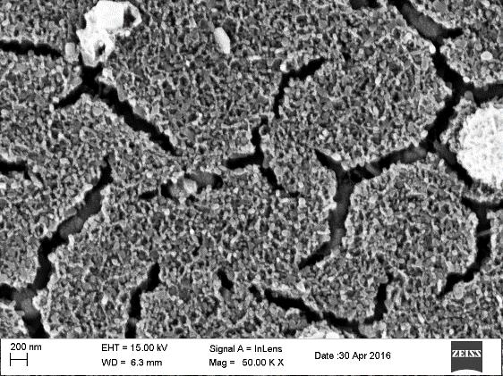
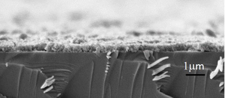
27 Analysis of the XRD pattern of the sulfurized samples indicates the formation of single phase kesterite Cu 2 ZnSnS 4 of tetragonal structure, as confirmed from the JCPDS (Joint Committee on Powder Diffraction Standards) database with card number [JCPDS Card: ]. The peaks located at 2θ values of , and respectively corresponding to the reflection from the (112), (220) and (312) planes of CZTS are characteristics of the 'kesterite' structure. The Miller indices, the values of the inter-planar spacing (d) of the reported (JCPDS) and calculated (this work) ones, and the reported relative intensities (I/I 0 ) of the diffraction lines are given in Table 3.1. It was found that the JCPDS values and the calculated inter-planar spacing values of this work are in good agreement with each other. Given the inter-planar spacing for a tetragonal system d = [((h 2 +k 2 )/a 2 ) + (l 2 /c 2 )] -1/2, the lattice constants of the crystals have been determined. The lattice constants 'a', 'b' and 'c' of the CZTS crystals are a = Å, b = Å. and c = Å. Table 3.1 X-ray thin film diffraction data for CZTS crystal (hkl) d hkl (Ǻ) (this work) d hkl (Ǻ) (JCPDS data) I/I 0 (%) (JCPDS data) Evaluation of surface and cross-sectional microstructure The surface and cross-sectional microstructure of the as-deposited and sulfurized samples were examined by FESEM as mentioned in chapter 2. The SEM micrographs corresponding to the as-deposited sample is shown in Figure 3.2. At low magnification, the film appears to be continuous and fully covers the substrate. Some occasional particulates (lighter contrast in the micrographs) are also visible. However, as the magnification was increased, a uniform mesh-like surface structure was observed. The particulate aggregates on the surface are also of same microstructure. The cross-sectional image shows the thickness to be about 210 nm. 20


28 Figure 3.2: Typical surface and cross-sectional FESEM images of the as-deposited films. However, as the samples were sulfurized, the microstructure of the samples were drastically changed. The surface and cross-sectional images of the films sulfurized at 400 and 450 ºC are shown in Figure 3.3 and 3.4 respectively. 21


29 Figure 3.3: Typical surface and cross-sectional FESEM images of the film sulfurized at 400 ºC. 22


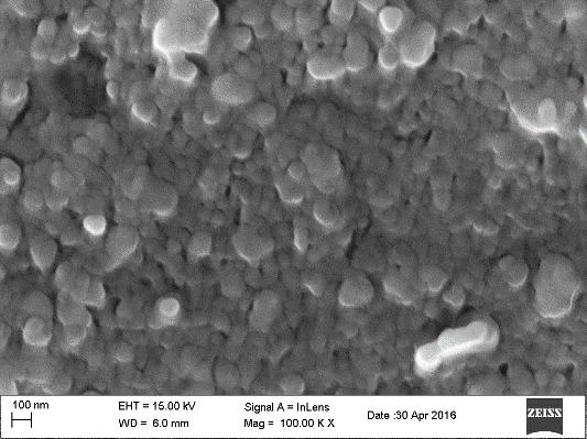
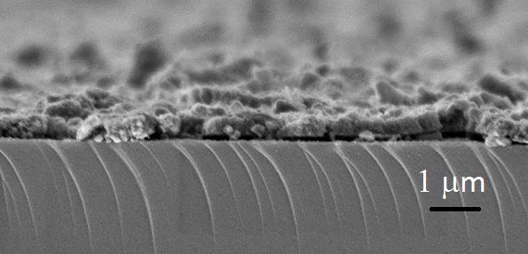
30 Figure 3.4: Typical surface and cross-sectional FESEM images of the film sulfurized at 450 ºC. 23
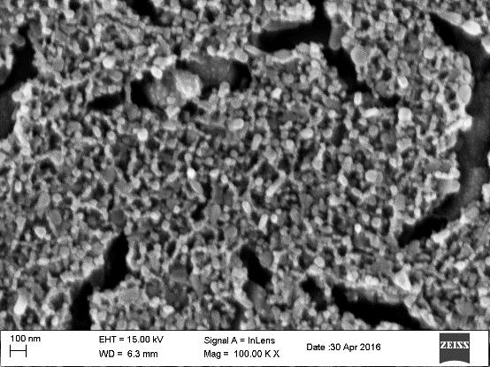
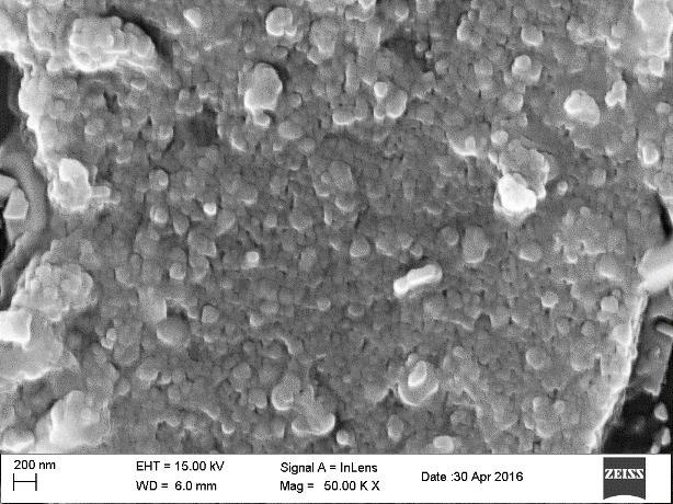
31 Transmittance (%) The sample sulfurized at 400 ºC still showed the mesh-like structure (as observed in the as-deposited sample), albeit improved compactness. At higher magnification, crystallization of the sample in the form of nearly-spherical particles were observed. The cross-sectional image showed that the thickness of the sample doubled to about 490 nm. However, there were many cracks in the films. Some of the cracks were isolated ones while many formed a continuous network in the films. As the sulfurization temperature was increased to 450 ºC, the mesh-like microstructure completely disappeared. The film was fully crystallized, as evident from higher magnification SEM micrographs. Locally, the film appeared to be well-crystallized. However, the film was completely discontinuous, and as the cross-sectional image shows, had been detached from the substrate at some places. 3.3 Optical studies Optical properties of the as-deposited and sulfurized CZTS thin films were studied from the UV-visible transmittance curves. Figures 3.5 shows typical transmittance curves of the films grown on the glass substrates as-deposited 450 C 400 C Wavelength (nm) Figure 3.5 Optical transmittance curves of the as-deposited and sulfurized CZTS films. 24
32 The as-deposited film showed visible transmittance of around 80 % in the wavelength range of nm. The high transmittance could be due to the porous mesh-like microstructure as revealed from the SEM micrographs (Figure 3.2) that allowed much of the incident photons to pass through the film. Since the XRD measurement did not reveal formation of any crystalline phase, analysis of the spectrum to estimate the bandgap appears unwise. The film synthesized at 400 ºC, showed considerably lower transmittance, which is similar to the reports available in literature. However, the crystallinity of this film was poor as evidenced from low intensity Bragg peaks in the XRD pattern as well as from SEM micrographs. The film sulfurized at 450 ºC also showed a similar trend. Surprisingly, the sulfurized films showed significant transmittance in the small wavelength region, where it was expected to be nearly zero since the band gap of the CZTS is about 1.5 ev. However, no conclusion could be drawn with the limited data of XRD, SEM and the UV-visible transmittance. 25
33 CHAPTER 4 SUMMARY AND FUTURE SCOPE The aim of this thesis was to fabricate and characterize Cu 2 ZnSnS 4 (CZTS) thin films. As there are many methods to prepare the films, we used a cost-competitive method to prepare the films. Chemical bath deposition (CBD) technique is used for this purpose as it is easy to carry out, setup is inexpensive and large area deposition is possible. We have used copper chloride, zinc chloride, tin chloride and thioacetamine (TAA) as ion sources and MEA as stabilizing agent. Ethanol was used as the solvent. All films were deposited on soda lime glass (SLG) substrates for required temperature for definite time period. It was intended to prepare the films at relatively low temperature from the industrial point of view to reduce the cost. Different films are prepared using different annealing temperatures to obtain crystalline CZTS absorber layer. For characterization purpose various techniques such as XRD, FE-SEM and UV-visible spectroscopy are used. From the XRD analysis, it is seen that on increasing annealing temperature, the polycrystallinity was improved. The results obtained at C are in good agreement with the standard results. The FE-SEM images showed that the as-deposited films had a mesh-like surface microstructure. However, at C, the mesh-like structure disappeared with the appearance of well-defined crystallites. From optical analysis, transmittance of the films was observed to be 80 % for as-deposited film in the wavelength range of nm. The present work demonstrates that although coating from a single dip followed by sulfurization at 450 C yields polycrystalline CZTS films, the films were discontinuous and had sub-micrometer particle size. Hence, further processing in the form of multiple coating is required for developing microstructure suitable for photovoltaic applications. The future scope of this work should include the optimization of process parameter including number of dip, duration of each dip, and post-deposition heat treatment. 26
34 References [1]. Peter Wurfel. Physics of Solar Cells: From Principles to New Concepts. Weinheim: Wiley, [2]. M. I. Khan, A. Kumar, A. Sharma and P. V. Singh. 2013, JECET, Vol. 2, p. 46. [3]. G. D. Rai, Non-Conventional energy sources. New Delhi: Khanna, [4]. R. F. Service. 2005, Science, Vol. 309, p [5]. Report of the Basic Energy Sciences Workshop on Solar Energy Utilization, US-DOE, April [6]. R. Eisenberg and D. G. Nocera. 2006, Inorg. Chem, Vol. 45, p [7]. A. R. Jha.Solar Cell Technology and Applications. Boca Raton: Auerbach, [8]. M. A. Green. 2007, J Mater Sci: Mater Electron, Vol. 18, p. 15. [9]. Lewis Fraas and Larry Partain, Solar cells and their applications. New Jersey: Wiley, [10]. J. B. Li, V. Chawla and B. M. Clemens. 2012, Adv Mater, Vol. 24, p [11]. B. R. Pamplin. 1960, Nature, Vol. 188, p [12]. P. Jackson, D. Hariskos, R. Wuerz, W. Wischmann, M. Powalla, Physica Status Solidi (Rapid Research Letters) 8, 219 (2014). [13]. [14]. [15]. [16]. H. Katagiri, K. Jimbo, W. S. Maw, K. Oishi, M. Yamazaki, H. Araki, and A. Takeuchi, Thin Solid Films, 517, 2455 (2009). [17]. D. B. Mitzi, O. Gunawan, T. K. Todorov, K. Wang, and S. Guha, Sol. Energy Mat. Sol. Cells, 95, 1421 (2011). [18]. H. Katagiri, K. Jimbo, S. Yamada, T. Kamimura, W. S. Maw, T. Fukano, T. Ito, and T. Motohiro, Appl. Phys. Express, 1, /1 (2008). [19]. W. Wang, M. T. Winkler, O. Gunawan, T. Gokmen, T.K. Todorov, Y. Zhu, and D. B. Mitzi, Adv. Energy Mater., 4, (2014). [20]. L. A. Wahab, M. B. El-Den, A. A. Farrag, S. A. Fayek and K. H. Marzouk. 2009, J. Phys. Chem. Solids, Vol. 70, p. 604 [21]. J. Zhang, L. Shao, Y. Fu and E. Xie. 2006, Rare metals, Vol. 25, p
35 [22]. S. R. Hall, J. T. Szymanski and J. M. Stewart. The Canadian Mineralogist, 16(2), , [23]. S. Schorr. 2007, Thin Solid Films, Vol. 515, p [24]. T. Maeda, S. Nakamura and T. Wada. 2009, In: Mater. Res. Soc. Symp. Proc., p [25]. S. R. Hall, J. T. Szymanski and J. M. Stewart. 1978, In: Canadian Mineralogist, Vol. 16, p [26]. D. R. Lide.Handbook of Chemistry and Physics. 79th. s.l. : CRC press, [27]. T. Washio, H. Nozaki, T. Fukano, T. Motohiro, K. Jimbo and H. katagiri. 2011, J. Appl. Phys., Vol. 110, p [28]. S. Chen, J. Yang, X. G. Gong, A. Walsh and S. Wei. 2010, Phys. Rev. B, Vol. 81, p (1). [29]. J. Zhang and L. Shao. 2009, Sci. China Ser. E:Tech. Sci., Vol. 52, p. 269 [30]. Y. B. Kishore Kumar, P. uday Bhaskar, G. Suresh babu and V. Sundara raja. 2010, Phys. Status Solidi A, Vol. 207, p [31]. N. Nakayama and K. Ito. 1996, Appl. Surf. Sci., Vol. 92, p [32]. T. Tanaka, T. Nagatomo, D. kawasaki, M. Nishio, Q. Guo, A. Wakahara, A. Yoshida and H. Ogawa. 2005, J. Phys. Chem. Solids, Vol. 66, p [33]. K. Moriya, K. Tanaka and H. Uchiki. 2008, Jpn. J. Appl. Phys., Vol. 47, p [34]. H. Katagiri, N. Sasaguchi, S. Hando, S. Hoshino, J. Ohashi and T. Yokota. 1997, Sol. Energy Mater. Sol. Cells, Vol. 49, p [35]. T. K. Chaudhari and D. Tiwari. 2012, Sol. Energy Mater. Sol. Cells, Vol. 101, p. 46. [36]. P. A. Fernandes, P. M. P. Salome, A. F. da Cunha and B. Schubert. 2010, Thin Solid Films, Vol. 519, p [37]. V. G. Rajeshmon, C. Sudha Kartha, K. P. Vijayakumar, C. Sanjeeviraja, T. Abe and Y. Kashiwaba. 2011, Sol. Energy, Vol. 85, p [38]. K. Ito and T. Nakazawa. 1988, Jpn. J. Appl. Phys., Vol. 27, p [39]. F. Liu, Y. Li, K. Zhang, B. Wang, C. Yan, Y. Lai, Z. Zhang, J. Li and Y. Liu. 2010, Sol. Energy Mater. Sol. Cells, Vol. 94, p [40]. C. P. Chan, H. Lam and C. Surya. 2010, Sol. Energy Mater. Sol. Cells, Vol. 94, p [41]. W. Xinkun, L. Wei, C. Shuying, L. Yunfeng and J. Hongjie. 2012, J. Semicond., Vol. 33, p
36 [42]. S. Chen, X. G. Gong, A. Walsh and S. Wei. 2009, Appl. Phys. Lett., Vol. 94, p [43]. J. Seol, S. Lee, J. Lee, H. Nam and K. Kim. 2003, Sol. Energy mater. Sol. Cells, Vol. 75, p [44]. K. Moriya, J. Watabe, K. Tanaka and H. Uchiki. 2006, Phys. status solidi (c), Vol. 3, p [45]. K. Sekiguchi, K. Tanaka, K. Moriya and H. Uchiki. 2006, Phys. status solidi (c), Vol. 3, p [46]. T. Prabhakar and J. Nagaraju. s.l. : Proceedings of the IEEE 35 th Photovoltaic Specialist Conference,Hawaii, USA, p [47]. K. Tanaka, N. Moritake, M. Oonuki and H. Uchiki. 2008, Jpn. J. Appl. Phys., Vol. 47, p [48]. P. A. Fernandes, P. M. P. Salome and A. F. da Cunha. 2011, J. Alloys Compd., Vol. 509, p [49]. Y. Cui, S. Zuo, J. Jiang, S. Yuan and J. Chu. 2011, Sol. Energy Mater. Sol. Cells, Vol. 95, p [50]. J. P. Leitao, N. M. Santos, P. A. Fernandes, P. M. P. Salome, A. F. da Cunha, J. C. Gonzalez, G. M. Ribeiro and F. M. Matinaga. 2011, Phys. Rev. B, Vol. 84, p [51]. J. P. Leitao, N. M. Santos, P. A. Fernandes, P. M. P. Salome, A. F. da Cunha, J. C. Gonzalez and Fs. M. Matinaga. 2011, Thin Solid Films, Vol. 519, p [52]. K. Ito, T. Nakazawa, Jpn. J. Appl. Phys. 27, 2094 (1988). [53]. H. Katagiri, N. Sasaguchi, S. Hando, S. Hoshino, J. Ohashi, and T. Yokota, Sol. Energy Mater. Sol.Cells, 49, 407 (1997). [54]. T. M. Friedlmeier, N. Wieser, T. Walter, H. Dittrich, and H. W. Schock, p. 1242, Bedford, UK, [55]. H. Katagiri, et al., Tech. Dig. Photovoltaic Science and Engineering Conf.-11, Sapporo, (1999) p.647. [56]. H. Katagiri, et al., Proc. World Conf. on Photovoltaic Energy Conversion-3, Osaka, (2003) p [57]. K. Todorov, K. B. Reuter, and D. B. Mitzi, Advanced Materials, vol. 22, no. 20, pp. E156 E159, View at Publisher View at Google Scholar View at Scopus [58]. Q. Guo, H. W. Hillhouse and R. Agrawal, J. Am. Chem. Soc., 131, (2009). 29
Applications of Successive Ionic Layer Adsorption and Reaction (SILAR) Technique for CZTS Thin Film Solar Cells
 Technique for CZTS Thin Film Solar Cells") NANO VISION An International Open Free Access, Peer Reviewed Research Journal www.nano-journal.org ISSN 2231-2579 (Print) ISSN 2319-7633 (Online) Abbr: Nano Vision. 2013, Vol.3(3): Pg.235-239 Applications
NANO VISION An International Open Free Access, Peer Reviewed Research Journal www.nano-journal.org ISSN 2231-2579 (Print) ISSN 2319-7633 (Online) Abbr: Nano Vision. 2013, Vol.3(3): Pg.235-239 Applications
Growth and Characterization of Cu 2 znsns 4 Thin Film by RF-Magnetron Sputtering
 Growth and Characterization of Cu 2 znsns 4 Thin Film by RF-Magnetron Sputtering V. Parthibaraj, K. Tamilarasan, K. S. Pugazhvadivu, C. Rangasami Department of Physics, Kongu Engineering College, Perundurai,
The next thin-film PV technology we will discuss today is based on CIGS.
 ET3034TUx - 5.3 - CIGS PV Technology The next thin-film PV technology we will discuss today is based on CIGS. CIGS stands for copper indium gallium selenide sulfide. The typical CIGS alloys are heterogeneous
CHAPTER 4. SYNTHESIS OF ALUMINIUM SELENIDE (Al 2 Se 3 ) NANO PARTICLES, DEPOSITION AND CHARACTERIZATION
 NANO PARTICLES, DEPOSITION AND CHARACTERIZATION") 40 CHAPTER 4 SYNTHESIS OF ALUMINIUM SELENIDE (Al 2 Se 3 ) NANO PARTICLES, DEPOSITION AND CHARACTERIZATION 4.1 INTRODUCTION Aluminium selenide is the chemical compound Al 2 Se 3 and has been used as a precursor
40 CHAPTER 4 SYNTHESIS OF ALUMINIUM SELENIDE (Al 2 Se 3 ) NANO PARTICLES, DEPOSITION AND CHARACTERIZATION 4.1 INTRODUCTION Aluminium selenide is the chemical compound Al 2 Se 3 and has been used as a precursor
DEVICE BEHAVIOR OF CZTSE/SI NANOWIRE HETEROJUNCTION
 PHOTOVOLTAIC TECHNICAL CONFERENCE - FROM ADVANCED MATERIALS AND PROCESSES TO INNOVATIVE APPLICATIONS 2017- DEVICE BEHAVIOR OF CZTSE/SI NANOWIRE HETEROJUNCTION G. Surucu 1,2,3, Ö. Bayraklı 2,3,4, H. H.
Synthesis and Characterization of Zinc Iron Sulphide (ZnFeS) Of Varying Zinc Ion Concentration
 Of Varying Zinc Ion Concentration") International Journal of Science and Technology Volume 5 No. 5, May, 2016 Synthesis and Characterization of Zinc Iron Sulphide (ZnFeS) Of Varying Zinc Ion Concentration I. B. Obasi 1 and J. C. Osuwa 2
International Journal of Science and Technology Volume 5 No. 5, May, 2016 Synthesis and Characterization of Zinc Iron Sulphide (ZnFeS) Of Varying Zinc Ion Concentration I. B. Obasi 1 and J. C. Osuwa 2
13.4 Chalcogenide solar cells Chalcopyrite solar cells
 13. Thin-Film Solar Cells 201 Figure 13.19: The crystal structure of copper indium diselenide, a typical chalcopyrite. The colors indicate copper (red), selenium (yellow) and indium (blue). For copper
Investigating the effect of Sodium and Potassium on the formation of Copper Zinc. Tin Sulfide Films. Cody Wrasman
 Investigating the effect of Sodium and Potassium on the formation of Copper Zinc Tin Sulfide Films Cody Wrasman INTRODUCTION As of 2008, global energy consumption reached 15 TW and is expected to double
Polycrystalline and microcrystalline silicon
 6 Polycrystalline and microcrystalline silicon In this chapter, the material properties of hot-wire deposited microcrystalline silicon are presented. Compared to polycrystalline silicon, microcrystalline
Photovoltaic Study of CZTS Thin Films Grown by Vacuum Evaporation and Chemical Bath Deposition Methods
 Nano Vision, Vol. 5(7-9), 169-176, July-September 2015 (An International Research Journal of Nano Science & Technology), www.nano-journal.org ISSN 2231-2579 (Print) ISSN 2319-7633 (Online) Photovoltaic
Growth Of TiO 2 Films By RF Magnetron Sputtering Studies On The Structural And Optical Properties
 Journal of Multidisciplinary Engineering Science and Technology (JMEST) Growth Of TiO 2 Films By RF Magnetron Sputtering Studies On The Structural And Optical Properties Ahmed K. Abbas 1, Mohammed K. Khalaf
Influence of In/Sn ratio on nanocrystalline indium tin oxide thin films by spray pyrolysis method
 Available online at www.scholarsresearchlibrary.com Scholars Research Library Archives of Physics Research, 2011, 2 (1): 19-25 (http://scholarsresearchlibrary.com/archive.html) ISSN 0976-0970 CODEN (USA):
Deposited by Sputtering of Sn and SnO 2
 Journal of the Korean Ceramic Society Vol. 49, No. 5, pp. 448~453, 2012. http://dx.doi.org/10.4191/kcers.2012.49.5.448 Comparative Study of Nitrogen Incorporated SnO 2 Deposited by Sputtering of Sn and
QUANTUM SIZE EFFECT IN CHEMOSYNTHESIZED NANOSTRUCTURED CdS THIN FILMS
 Digest Journal of Nanomaterials and Biostructures Vol. 5, No 4, October-December 2010, p. 805-810 QUANTUM SIZE EFFECT IN CHEMOSYNTHESIZED NANOSTRUCTURED CdS THIN FILMS S. A. VANALAKAR, S. S. MALI, M. P.
Effect Thickness and Temperature Annealing on Structural and Optical Proportion of CuInTe 2 Thin Film
 AASCIT Journal of Materials 2016; 2(1): 1-5 Published online February 24 2016 (http://www.aascit.org/journal/materials) Effect Thickness and Temperature Annealing on Structural and Optical Proportion of
Basics of Solar Photovoltaics. Photovoltaics (PV) Lecture-21
 Lecture-21") Lecture-21 Basics of Solar Photovoltaics Photovoltaics (PV) Photovoltaics (PV) comprise the technology to convert sunlight directly into electricity. The term photo means light and voltaic, electricity.
Lecture-21 Basics of Solar Photovoltaics Photovoltaics (PV) Photovoltaics (PV) comprise the technology to convert sunlight directly into electricity. The term photo means light and voltaic, electricity.
Cu(In,Ga)Se 2 FILM FORMATION FROM SELENIZATION OF MIXED METAL/METAL-SELENIDE PRECURSORS
Se 2 FILM FORMATION FROM SELENIZATION OF MIXED METAL/METAL-SELENIDE PRECURSORS") Cu(In,Ga)Se 2 FILM FORMATION FROM SELENIZATION OF MIX METAL/METAL-SELENIDE PRECURSORS Rui Kamada, William N. Shafarman, and Robert W. Birkmire Institute of Energy Conversion University of Delaware, Newark,
Cu(In,Ga)Se 2 FILM FORMATION FROM SELENIZATION OF MIX METAL/METAL-SELENIDE PRECURSORS Rui Kamada, William N. Shafarman, and Robert W. Birkmire Institute of Energy Conversion University of Delaware, Newark,
Deposition of Cu 2 ZnSnS 4 (CZTS) prepared by a solution route for solar cells applications
 prepared by a solution route for solar cells applications") Deposition of Cu ZnSnS 4 (CZTS) prepared by a solution route for solar cells applications J. H. Nkuissi Tchognia 1, *, Y. Arba 1, B. Hartiti 1, K. Dakhsi 1, J.M. Ndjaka, A. Ridah 1, P. Thevenin 3 1 MAC
Deposition of Cu ZnSnS 4 (CZTS) prepared by a solution route for solar cells applications J. H. Nkuissi Tchognia 1, *, Y. Arba 1, B. Hartiti 1, K. Dakhsi 1, J.M. Ndjaka, A. Ridah 1, P. Thevenin 3 1 MAC
An advantage of thin-film silicon solar cells is that they can be deposited on glass substrates and flexible substrates.
 ET3034TUx - 5.2.1 - Thin film silicon PV technology 1 Last week we have discussed the dominant PV technology in the current market, the PV technology based on c-si wafers. Now we will discuss a different
Effect of Volume Spray Rate on Highly Conducting Spray Deposited Fluorine Doped SnO2 Thin Films
 Effect of Volume Spray Rate on Highly Conducting Spray Deposited Fluorine Doped SnO2 Thin Films Dr.R.N. ARLE 1, B.L.KHATIK 2 1 Department of Physics, Jijamata College of Science and Arts, Bhende Bk.India
Synthesis and Characterization of Copper-Zinc-Tin-Sulfide (CZTS) Thin Film Absorber Layer for Solar Cell Application
 Thin Film Absorber Layer for Solar Cell Application") Journal of Materials Science and Engineering A 8 (9-10) (2018) 198-203 doi: 10.17265/2161-6213/2018.9-10.004 D DAVID PUBLISHING Synsis and Characterization of Copper-Zinc-Tin-Sulfide (CZTS) Thin Film Absorber
Journal of Materials Science and Engineering A 8 (9-10) (2018) 198-203 doi: 10.17265/2161-6213/2018.9-10.004 D DAVID PUBLISHING Synsis and Characterization of Copper-Zinc-Tin-Sulfide (CZTS) Thin Film Absorber
Effect of CZTS Parameters on Photovoltaic Solar Cell from Numerical Simulation
 Journal of Energy and Power Engineering 13 (2019) 32-36 doi: 10.17265/1934-8975/2019.01.003 D DAVID PUBLISHING Effect of CZTS Parameters on Photovoltaic Solar Cell from Numerical Simulation Abdellah Benami
This version was downloaded from Northumbria Research Link:
 Citation: Zoppi, Guillaume, Forbes, Ian, Miles, Robert, Dale, Phillip, Scragg, Jonathan and Peter, Laurence (9) Quaternary CuZnSnSe4 thin films for solar cells applications. In: 5th Photovoltaic Science
STRUCTURAL AND OPTOELECTRONIC PROPERTIES OF PYRALYTICALLY SPRAYED CdZnS THIN FILMS
 Chalcogenide Letters Vol. 9, No. 12, December 2012, p. 495-500 STRUCTURAL AND OPTOELECTRONIC PROPERTIES OF PYRALYTICALLY SPRAYED CdZnS THIN FILMS S. RAJATHI *, N. SANKARASUBRAMANIAN *, K. RAMANATHAN, M.
Optical parameter determination of ZrO 2 thin films prepared by sol gel dip coating
 International Journal of ChemTech Research CODEN (USA): IJCRGG ISSN : 0974-490 Vol.6, No.13, pp 534-5346, November 014 MESCon 014 [4th -5 th September 014] National Conference on Material for Energy Storage
Texture inheritance in thin film growth of Cu 2 ZnSnS 4
 Texture inheritance in thin film growth of Cu 2 ZnSnS 4 A. Weber *, S. Schmidt, D. Abou-Ras, P. Schubert-Bischoff, I. Denks, R. Mainz, H.W. Schock Helmholtz-Zentrum Berlin für Materialien und Energie,
OPTIMIZATION OF ZINC SULFIDE (ZnS) ELECTRON AFFINITY IN COPPER INDIUM SULFIDE (CIS) BASED PHOTOVOLTAIC CELL
 ELECTRON AFFINITY IN COPPER INDIUM SULFIDE (CIS) BASED PHOTOVOLTAIC CELL") Chalcogenide Letters Vol. 10, No. 6, June 2013, p. 189-195 OPTIMIZATION OF ZINC SULFIDE (ZnS) ELECTRON AFFINITY IN COPPER INDIUM SULFIDE (CIS) BASED PHOTOVOLTAIC CELL HADIBAH RAMLI a*, SHARUL KAMAL ABDUL
Chalcogenide Letters Vol. 10, No. 6, June 2013, p. 189-195 OPTIMIZATION OF ZINC SULFIDE (ZnS) ELECTRON AFFINITY IN COPPER INDIUM SULFIDE (CIS) BASED PHOTOVOLTAIC CELL HADIBAH RAMLI a*, SHARUL KAMAL ABDUL
Deposition and Characterization of Cu2ZnSnS4 Thin Films for Solar Cell Applications
 Deposition and Characterization of Cu2ZnSnS4 Thin Films for Solar Cell Applications Nabeel A. Bakr*, Sabah A. Salman, Sabreen A. Hameed Department of Physics, College of Science, University of Diyala,
Production of Homogeneous Cu 2 ZnSnS 4 by Splat Solidification in Microgravity
 (S72 S77) 8th Japan-China-Korea Workshop on Microgravity Sciences for Asian Microgravity Pre-Symposium Production of Homogeneous Cu 2 ZnSnS 4 by Splat Solidification in Microgravity Tatsuya NAKAZAWA 1,
Ceramic Processing Research
 Journal of Ceramic Processing Research. Vol. 10, No. 4, pp. 536~540 (009) J O U R N A L O F Ceramic Processing Research Electrical and optical properties of MgO films deposited on soda lime glass by a
PHOTO-ELECTROCHEMICAL PROPERTIES OF FLASH EVAPORATED CADMIUM SULPHIDE FILMS
 Chalcogenide Letters Vol. 5, No. 9, September 2008, p. 195-199 PHOTO-ELECTROCHEMICAL PROPERTIES OF FLASH EVAPORATED CADMIUM SULPHIDE FILMS K. R. Murali *, C. Kannan a, P. K. Subramanian b Electrochemical
Structural and optical characterization of reactive evaporated tin diselenide thin films
 IOP Conference Series: Materials Science and Engineering OPEN ACCESS Structural and optical characterization of reactive evaporated tin diselenide thin films Recent citations - Studies on Physical Properties
Structural and Electrical Properties of CIAGS Thin Films
 Structural and Electrical Properties of CIAGS Thin Films *Saira Riaz 1), Anam Azam 2), Usman Khan 2) and Shahzad Naseem 1) 1), 2) Centre of Excellence in Solid State Physics, University of the Punjab,
The growth of patterned ceramic thin films from polymer precursor solutions Göbel, Ole
 University of Groningen The growth of patterned ceramic thin films from polymer precursor solutions Göbel, Ole IMPORTANT NOTE: You are advised to consult the publisher's version (publisher's PDF) if you
for New Energy Materials and Devices; Beijing National Laboratory for Condense Matter Physics,
 Electronic Supplementary Information Highly efficient core shell CuInS 2 /Mn doped CdS quantum dots sensitized solar cells Jianheng Luo, a Huiyun Wei, a Qingli Huang, a Xing Hu, a Haofei Zhao, b Richeng
KGC SCIENTIFIC TYPES OF SOLAR CELL
 KGC SCIENTIFIC www.kgcscientific.com TYPES OF SOLAR CELL How Photovoltaic Cell Work When sunshine that contain photon strike the panel, semiconductor material will ionized Causing electron to break free
Synthesis and Characterization of Cadmium Sulfide (CdS) Quantum Dots (QDS) for Quantum Dot Sensitized Solar Cell Applications
 Quantum Dots (QDS) for Quantum Dot Sensitized Solar Cell Applications") Nano Vision, Vol. 5(7-9), 237-241, July-September 2015 (An International Research Journal of Nano Science & Technology), www.nano-journal.org ISSN 2231-2579 (Print) ISSN 2319-7633 (Online) Synthesis and
Nano Vision, Vol. 5(7-9), 237-241, July-September 2015 (An International Research Journal of Nano Science & Technology), www.nano-journal.org ISSN 2231-2579 (Print) ISSN 2319-7633 (Online) Synthesis and
GROWTH AND CHARACTERIZATION OF NANOSTRUCTURED CdS THIN FILMS BY CHEMICAL BATH DEPOSITION TECHNIQUE
 Chalcogenide Letters Vol. 6, No. 8, September 29, p. 415 419 GROWTH AND CHARACTERIZATION OF NANOSTRUCTURED CdS THIN FILMS BY CHEMICAL BATH DEPOSITION TECHNIQUE V. B. SANAP *, B. H. PAWAR, * MSS s College
Synthesis and Characterization of DC Magnetron Sputtered ZnO Thin Films Under High Working Pressures
 Accepted Manuscript Synthesis and Characterization of DC Magnetron Sputtered ZnO Thin Films Under High Working Pressures M. Hezam, N. Tabet, A. Mekki PII: S0040-6090(10)00417-7 DOI: doi: 10.1016/j.tsf.2010.03.091
GROWTH, STRUCTURE AND OPTICAL CHARACTERIZATION OF CuGaS 2 THIN FILMS OBTAINED BY SPRAY PYROLYSIS
 Chalcogenide Letters Vol. 12, No. 3, March 2015, p. 111-116 GROWTH, STRUCTURE AND OPTICAL CHARACTERIZATION OF CuGaS 2 THIN FILMS OBTAINED BY SPRAY PYROLYSIS S. LIU *, L. NIE, R. YUAN School of Chemistry
High Efficiency Heterojunction Cadmium Sulphide (CdS) Thin Film Solar Cells by Thermal Evaporation Technique
 Thin Film Solar Cells by Thermal Evaporation Technique") NANO VISION An International Open Free Access, Peer Reviewed Research Journal www.nano-journal.org ISSN 2231-2579 (Print) ISSN 2319-7633 (Online) Abbr: Nano Vision. 2013, Vol.3(3): Pg.179-183 High Efficiency
NANO VISION An International Open Free Access, Peer Reviewed Research Journal www.nano-journal.org ISSN 2231-2579 (Print) ISSN 2319-7633 (Online) Abbr: Nano Vision. 2013, Vol.3(3): Pg.179-183 High Efficiency
SOLAR ENERGY. Approximately 120,000 TW of solar energy strikes the earth s surface, capturing only a fraction could supply all of our energy needs.
 SOLAR ENERGY Approximately 120,000 TW of solar energy strikes the earth s surface, capturing only a fraction could supply all of our energy needs. What is Photovoltaics? Photovoltaics is a high-technology
Structure and optical properties of M/ZnO (M=Au, Cu, Pt) nanocomposites
 nanocomposites") Solar Energy Materials & Solar Cells 8 () 339 38 Structure and optical properties of M/ (M=Au, Cu, Pt) nanocomposites U. Pal a,b, *, J. Garc!ıa-Serrano a, G. Casarrubias-Segura a, N. Koshizaki c, T. Sasaki
Solar Energy Materials & Solar Cells 8 () 339 38 Structure and optical properties of M/ (M=Au, Cu, Pt) nanocomposites U. Pal a,b, *, J. Garc!ıa-Serrano a, G. Casarrubias-Segura a, N. Koshizaki c, T. Sasaki
Growth and Characterization of Cd 1-x Zn x Te Films
 Universities Research Journal 2011, Vol. 4, No. 4 Growth and Characterization of Cd 1-x Zn x Te Films Nway Han Myat Thin 1 and Pho Kaung 2 Abstract The II-VI polycrystalline semiconducting materials have
This version was downloaded from Northumbria Research Link:
 Citation: Maiello, Pietro, Zoppi, Guillaume, Miles, Robert, Pearsall, Nicola and Forbes, Ian (2011) Investigations of ternary Cu3SbS3 thin films as absorber in photovoltaic devices. In: The 7th Photovoltaic
DIELECTRIC AND IMPEDANCE STUDY OF OPTIMIZED CADMIUM SULPHIDE THIN FILM
 Chalcogenide Letters Vol. 1, No. 1, January 213, p. 1-1 DIELECTRIC AND IMPEDANCE STUDY OF OPTIMIZED CADMIUM SULPHIDE THIN FILM K. S. OJHA a*, R. L. SRIVASTAVA b a Institute of Engineering & Technology,
Structural and Optical Properties of Aluminium Antimonide Thin Films Deposited By Thermal Evaporation Method
 Available online at www.scholarsresearchlibrary.com Scholars Research Library Archives of Physics Research, 2011, 2 (1): 146-153 (http://scholarsresearchlibrary.com/archive.html) ISSN 0976-0970 CODEN (USA):
ZnO-based Transparent Conductive Oxide Thin Films
 IEEE EDS Mini-colloquium WIMNACT 32 ZnO-based Transparent Conductive Oxide Thin Films Weijie SONG Ningbo Institute of Material Technology and Engineering, Chinese Academy of Sciences, Ningbo, P. R. China
Synthesis, Characterization and Optical Properties of ZnS Thin Films
 Synthesis, Characterization and Optical Properties of ZnS Thin Films H. R. Kulkarni KJ College of Engineering and Management Research, Pune, India Abstract: ZnS thin films were prepared by pulsed electrodeposition
Synthesis, Structural, Optical and Electrical Properties of Cadmium sulphide Thin Films by Chemical Bath Deposition Method
 International Journal of ChemTech Research CODEN (USA): IJCRGG ISSN : 0974-4290 Vol.6, No.7, pp 3748-3752, Sept-Oct 2014 Synthesis, Structural, Optical and Electrical Properties of Cadmium sulphide Thin
STUDY OF CHEMICAL BATH DEPOSITED NANOCRYSTALLINE CdZnS THIN FILMS
 Journal of Optoelectronics and Biomedical Materials Vol. 3 Issue 2, April-June 2011 p. 39-43 STUDY OF CHEMICAL BATH DEPOSITED NANOCRYSTALLINE CdZnS THIN FILMS V. B. SANAP *, B. H. PAWAR *Yeshwantrao Chavan
The Effect of Annealing Heat Treatment on Structural and Optical Properties of Ce-doped ZnO Thin Films
 4th International Conference on Computer, Mechatronics, Control and Electronic Engineering (ICCMCEE 2015) The Effect of Annealing Heat Treatment on Structural and Optical Properties of Ce-doped Thin Films
Nanoparticle Solar Cells
 Nanoparticle Solar Cells ECG653 Project Report submitted by Sandeep Sangaraju (sangaraj@unlv.nevada.edu), Fall 2008 1. Introduction: Solar cells are the most promising product in future. These can be of
ELECTRICAL PROPERTIES OF CDS THIN FILMS SPIN COATED ON CONDUCTIVE GLASS SUBSTRATES
 UDC: 538.9 Condensed matter Physics, Solid state Physics, Experimental Condensed matter Physics ELECTRICAL PROPERTIES OF CDS THIN FILMS SPIN COATED ON CONDUCTIVE GLASS SUBSTRATES P. Samarasekara and P.A.S.
Fabrication of CdTe thin films by close space sublimation
 Loughborough University Institutional Repository Fabrication of CdTe thin films by close space sublimation This item was submitted to Loughborough University's Institutional Repository by the/an author.
Mn DOPED SnO2 Semiconducting Magnetic Thin Films Prepared by Spray Pyrolysis Method
 International Journal of Scientific & Engineering Research Volume 2, Issue 4, April-2011 1 Mn DOPED SnO2 Semiconducting Magnetic Thin Films Prepared by Spray Pyrolysis Method K.Vadivel, V.Arivazhagan,
Structural, Optical and Surface Properties of CdTe Thin Films on CdS/FTO Glass Substrates
 American Journal of Materials Science and Application 2015; 3(6): 76-80 Published online November 2, 2015 (http://www.openscienceonline.com/journal/ajmsa) Structural, Optical and Surface Properties of
Accepted Manuscript. Cu 2 ZnSnS 4 thin films by sulfurization in melted sulfur. S.A. Bashkirov, U.S. Hekkel, M.S. Tivanov, A.M.
 Accepted Manuscript Cu 2 ZnSnS 4 thin films by sulfurization in melted sulfur S.A. Bashkirov, U.S. Hekkel, M.S. Tivanov, A.M. Saad PII: S0167-577X(18)30391-4 DOI: https://doi.org/10.1016/j.matlet.2018.03.035
CHAPTER 5. DEPOSITION AND CHARACTERIZATION OF ZINC STANNATE (Zn 2 SnO 4 ) THIN FILMS
 THIN FILMS") 106 CHAPTER 5 DEPOSITION AND CHARACTERIZATION OF ZINC STANNATE (Zn 2 SnO 4 ) THIN FILMS 5.1 INTRODUCTION Post-transition-metal oxides and their alloys have unique physical properties. Despite their large
106 CHAPTER 5 DEPOSITION AND CHARACTERIZATION OF ZINC STANNATE (Zn 2 SnO 4 ) THIN FILMS 5.1 INTRODUCTION Post-transition-metal oxides and their alloys have unique physical properties. Despite their large
CHAPTER 3. Experimental Results of Magnesium oxide (MgO) Thin Films
 Thin Films") CHAPTER 3 Experimental Results of Magnesium oxide (MgO) Thin Films Chapter: III ---------------------------------------------------------------- Experimental Results of Magnesium oxide (MgO) Thin Films
CHAPTER 3 Experimental Results of Magnesium oxide (MgO) Thin Films Chapter: III ---------------------------------------------------------------- Experimental Results of Magnesium oxide (MgO) Thin Films
Influence of Annealing Temperature on the Properties of ITO Films Prepared by Electron Beam Evaporation and Ion-Assisted Deposition
 Kasetsart J. (Nat. Sci.) 42 : 362-366 (2008) Influence of Annealing Temperature on the Properties of ITO Films Prepared by Electron Beam Evaporation and Ion-Assisted Deposition Artorn Pokaipisit 1 *, Mati
Numerical Simulation of Cu 2 ZnSnS 4 Based Solar Cells with In 2 S 3 Buffer Layers by SCAPS-1D
 Journal of Applied Science and Engineering, Vol. 17, No. 4, pp. 383 390 (2014) DOI: 10.6180/jase.2014.17.4.05 Numerical Simulation of Cu 2 ZnSnS 4 Based Solar Cells with In 2 S 3 Buffer Layers by SCAPS-1D
Comparative studies on XRD and band gap of thin films of gel grown, doped and undoped PbI 2, and pure powder of PbI 2
 Available online at www.scholarsresearchlibrary.com Scholars Research Library Archives of Applied Science Research, 11, 3 (3):65-71 (http://scholarsresearchlibrary.com/archive.html) ISSN 975-58X CODEN
International Journal of Engineering Research-Online A Peer Reviewed International Journal
 N C L A 2016 ISSN: 2321-7758 STUDY OF PHOTOVOLTAIC CHARACTERIZATION OF SPRAY DEPOSITED CdTe THIN FILMS D.M.Sapkal S.I.C.E.S. Degree college of Arts, Commerce & Science, Ambernath(west) ABSTRACT CdTe thin
Supporting Information. Solution-Processed 2D PbS Nanoplates with Residual Cu 2 S. Exhibiting Low Resistivity and High Infrared Responsivity
 Supporting Information Solution-Processed 2D PbS Nanoplates with Residual Cu 2 S Exhibiting Low Resistivity and High Infrared Responsivity Wen-Ya Wu, Sabyasachi Chakrabortty, Asim Guchhait, Gloria Yan
Synthesis and Characterization of Cadmium Sulfide Nanoparticles
 Synthesis and Characterization of Cadmium Sulfide Nanoparticles R.Hepzi Pramila Devamani 1*, R.Kiruthika, P.Mahadevi and S.Sagithapriya 2 1 1. Assistant Professor, Department of Physics, V.V.Vanniaperumal
ANNEALING EFFECT OF CUTE THIN FILMS
 (An International Peer Reviewed Journal), www.ijaconline.com, ISSN 973-2861 Volume XI, Issue I, Jan- October 218 ANNEALING EFFECT OF CUTE THIN FILMS A. Selvaraj & G. Kanchana Assistant Professor, Department
Growth of CZTS thin films by sulfurization of sputtered singlelayered Cu Zn Sn metallic precursors from an alloy target
 J Mater Sci: Mater Electron (2013) 24:4958 4963 DOI 10.1007/s10854-013-1507-5 Growth of CZTS thin films by sulfurization of sputtered singlelayered Cu Zn Sn metallic precursors from an alloy target Shanshan
Preparation of CuAlO 2 Thin Films by Sol-Gel Method Using Nitrate Solution Dip-Coating
 Preparation of CuAlO 2 Thin Films by Sol-Gel Method Using Nitrate Solution Dip-Coating Takashi Ehara 1,2,a* and Takayoshi Nakanishi 1 1 Department of Human Culture, Faculty of Human Studies, Ishinomaki
Research Article Optical and Electrical Properties of Ag-Doped In 2 S 3 Thin Films Prepared by Thermal Evaporation
 Advances in Materials Science and Engineering, Article ID 37861, 4 pages http://dx.doi.org/1.1155/214/37861 Research Article Optical and Electrical Properties of Ag-Doped In 2 S 3 Thin Films Prepared by
Solid-Phase Synthesis of Mg2Si Thin Film on Sapphire substrate
 Proc. Asia-Pacific Conf. on Semiconducting Silicides and Related Materials 2016 JJAP Conf. Proc. 5, https://doi.org/10.7567/jjapcp.5.011302 Solid-Phase Synthesis of Mg2Si Thin Film on Sapphire substrate
INVESTIGATION OF ALKALI ELEMENTAL DOPING EFFECTS ON SOLUTION PROCESSED Cu2ZnSn(S,Se)4 THIN FILMS FOR PHOTOVOLTAICS
4 THIN FILMS FOR PHOTOVOLTAICS") INVESTIGATION OF ALKALI ELEMENTAL DOPING EFFECTS ON SOLUTION PROCESSED Cu2ZnSn(S,Se)4 THIN FILMS FOR PHOTOVOLTAICS LI WENJIE SCHOOL OF MATERIALS SCIENCE AND ENGINEERING 2016 Investigation of Alkali Elemental
INVESTIGATION OF ALKALI ELEMENTAL DOPING EFFECTS ON SOLUTION PROCESSED Cu2ZnSn(S,Se)4 THIN FILMS FOR PHOTOVOLTAICS LI WENJIE SCHOOL OF MATERIALS SCIENCE AND ENGINEERING 2016 Investigation of Alkali Elemental
Rational defect passivation of Cu 2 ZnSn(S,Se) 4 photovoltaics with solution-processed Cu 2 ZnSnS 4 :Na nanocrystals
 4 photovoltaics with solution-processed Cu 2 ZnSnS 4 :Na nanocrystals") Supporting Information for Rational defect passivation of Cu 2 ZnSn(S,Se) 4 photovoltaics with solution-processed Cu 2 ZnSnS 4 :Na nanocrystals Huanping Zhou 1,2+, Tze-Bin Song 1,2+, Wan-Ching Hsu 1,2,
Supporting Information for Rational defect passivation of Cu 2 ZnSn(S,Se) 4 photovoltaics with solution-processed Cu 2 ZnSnS 4 :Na nanocrystals Huanping Zhou 1,2+, Tze-Bin Song 1,2+, Wan-Ching Hsu 1,2,
Influence of Thermal Annealing on the Structural and Optical Properties of Lead Oxide Thin Films Prepared by Chemical Bath Deposition Technique
 Influence of Thermal Annealing on the Structural and Optical Properties of Lead Oxide Thin Films Prepared by Chemical Bath Deposition Technique D.D.O. Eya, Ph.D. Department of Physics, Federal University
Effect of Doping Concentration on the Structural Properties of Zn: SnO 2
 IOSR Journal of Applied Physics (IOSR-JAP) e-issn: 2278-4861.Volume 7, Issue 3 Ver. II (May. - Jun. 2015), PP 45-49 www.iosrjournals.org Effect of Doping Concentration on the Structural Properties of Zn:
Recrystallization in CdTe/CdS
 Thin Solid Films 361±362 (2000) 420±425 www.elsevier.com/locate/tsf Recrystallization in CdTe/CdS A. Romeo, D.L. BaÈtzner, H. Zogg, A.N. Tiwari* Thin Film Physics Group, Institute of Quantum Electronics,
EFFECT OF DEPOSITION TIME ON CHEMICAL BATH DEPOSITION PROCESS AND THICKNESS OF BaSe THIN FILMS.
 Journal of Optoelectronics and Biomedical Materials Vol. 3 Issue 4, October-December 2011 p. 81-85 EFFECT OF DEPOSITION TIME ON CHEMICAL BATH DEPOSITION PROCESS AND THICKNESS OF BaSe THIN FILMS. N.A. OKEREKE
Contents. Abbreviations and Symbols... 1 Introduction... 1
 Contents Abbreviations and Symbols... XIII 1 Introduction... 1 2 Experimental Techniques... 5 2.1 Positron Sources... 7 2.2 Positron Lifetime Spectroscopy... 9 2.2.1 Basics of the Measurement... 10 2.2.2
INVESTIGATION ON STRUCTURAL, OPTICAL, MORPHOLOGICAL AND ELECTRICAL PROPERTIES OF LEAD SULPHIDE (PbS) THIN FILMS
 THIN FILMS") Journal of Ovonic Research Vol. 11, No. 3, May - June 015, p. 13-130 INVESTIGATION ON STRUCTURAL, OPTICAL, MORPHOLOGICAL AND ELECTRICAL PROPERTIES OF LEAD SULPHIDE (PbS) THIN FILMS S.THIRUMAVALAVAN a*,
Journal of Ovonic Research Vol. 11, No. 3, May - June 015, p. 13-130 INVESTIGATION ON STRUCTURAL, OPTICAL, MORPHOLOGICAL AND ELECTRICAL PROPERTIES OF LEAD SULPHIDE (PbS) THIN FILMS S.THIRUMAVALAVAN a*,
Crystalline Silicon Solar Cells
 12 Crystalline Silicon Solar Cells As we already discussed in Chapter 6, most semiconductor materials have a crystalline lattice structure. As a starting point for our discussion on crystalline silicon
Silver Diffusion Bonding and Layer Transfer of Lithium Niobate to Silicon
 Chapter 5 Silver Diffusion Bonding and Layer Transfer of Lithium Niobate to Silicon 5.1 Introduction In this chapter, we discuss a method of metallic bonding between two deposited silver layers. A diffusion
Optical, microstructural and electrical studies on sol gel derived TiO 2 thin films
 Indian Journal of Pure & Applied Physics Vol. 55, January 2017, pp. 81-85 Optical, microstructural and electrical studies on sol gel derived TiO 2 thin films M Bilal Tahir*, S Hajra, M Rizwan & M Rafique
Cu-Zn-Sn-S Thin Films from Electrodeposited Metallic Precursor Layers
 The Open Surface Science Journal, 212, 4, 19-24 19 Open Access Cu-Zn-Sn-S Thin Films from Electrodeposited Metallic Precursor Layers Raghu N. Bhattacharya * and J.Y. Kim National Renewable Energy Laboratory,
Effect of copper doping on the some physical properties of Nio thin films prepared by chemical spray pyrolysis
 Effect of copper doping on the some physical properties of Nio thin films prepared by chemical spray pyrolysis 1. Dr. Anwar H. Ali, 2. Raania R. Kadhim 1. Department of Physics College of science, Al-
Development of Cu 2 ZnSnS 4 absorber layer for thin film solar cell using chemical bath deposition technique
 FINAL REPORT OF THE MINOR PROJECT (MRP(S)/13-14/KLMG015/UGC-SWRO) Development of Cu 2 ZnSnS 4 absorber layer for thin film solar cell using chemical bath deposition technique Submitted by Dr. Rajeshmon
Fabrication of Cu 2 ZnSnSe 4 Thin-film Solar Cells by a Two-stage Process
 University of South Florida Scholar Commons Graduate Theses and Dissertations Graduate School 4-6-2016 Fabrication of Cu 2 ZnSnSe 4 Thin-film Solar Cells by a Two-stage Process Yejiao Wang Follow this
The Influence of Solvent Coordination on Hybrid. Organic-Inorganic Perovskite Formation. (Supporting Information)
") The Influence of Solvent Coordination on Hybrid Organic-Inorganic Perovskite Formation (Supporting Information) J. Clay Hamill, Jr., Jeffrey Schwartz, and Yueh-Lin Loo, * Department of Chemical and Biological
The Influence of Solvent Coordination on Hybrid Organic-Inorganic Perovskite Formation (Supporting Information) J. Clay Hamill, Jr., Jeffrey Schwartz, and Yueh-Lin Loo, * Department of Chemical and Biological
Advanced Analytical Chemistry Lecture 9. Chem 4631
 Advanced Analytical Chemistry Lecture 9 Chem 4631 Solar Cell Research Solar Cell Research Solar Cell Research Solar Cell Research Thin film technologies Candidates for thin-film solar cells: Crystalline
Amorphous Materials Exam II 180 min Exam
 MIT3_071F14_ExamISolutio Name: Amorphous Materials Exam II 180 min Exam Problem 1 (30 Points) Problem 2 (24 Points) Problem 3 (28 Points) Problem 4 (28 Points) Total (110 Points) 1 Problem 1 Please briefly
ANALYSIS ON ENERGY BANDGAP OF ZINC SULPHIDE (ZnS) THIN FILMS GROWN BY SOLUTION GROWTH TECHNIQUE
 THIN FILMS GROWN BY SOLUTION GROWTH TECHNIQUE") Chalcogenide Letters Vol. 14, No. 8, August 2017, p. 357-363 ANALYSIS ON ENERGY BANDGAP OF ZINC SULPHIDE (ZnS) THIN FILMS GROWN BY SOLUTION GROWTH TECHNIQUE P. E. AGBO a.b, P. A. NWOFE b*, L. O. ODO b,c
Chalcogenide Letters Vol. 14, No. 8, August 2017, p. 357-363 ANALYSIS ON ENERGY BANDGAP OF ZINC SULPHIDE (ZnS) THIN FILMS GROWN BY SOLUTION GROWTH TECHNIQUE P. E. AGBO a.b, P. A. NWOFE b*, L. O. ODO b,c
Size dependent optical characteristics of chemically deposited nanostructured ZnS thin films
 Bull. Mater. Sci., Vol. 30, No. 2, April 2007, pp. 147 151. Indian Academy of Sciences. Size dependent optical characteristics of chemically deposited nanostructured ZnS thin films A U UBALE*, V S SANGAWAR
Effect of deposition parameters on Structural and Optical Properties of ZnS Thin Films
 IOP Conference Series: Materials Science and Engineering PAPER OPEN ACCESS Effect of deposition parameters on Structural and Optical Properties of ZnS Thin Films To cite this article: K Priya et al 2018
BAND GAP SHIFT AND OPTICAL CHARACTERIZATION OF PVA-CAPPED PbO THIN FILMS: EFFECT OF THERMAL ANNEALING
 Chalcogenide Letters Vol. 8, No. 3, March 211, p.163 17 BAND GAP SHIFT AND OPTICAL CHARACTERIZATION OF PVA-CAPPED PbO THIN FILMS: EFFECT OF THERMAL ANNEALING P.U. ASOGWA * Department of Physics and Astronomy,
Studies on Structural and Optical Properties of Iron doped Cds Nanoparticles ABSTRACT
 Studies on Structural and Optical Properties of Iron doped Cds Nanoparticles Atheek P., Vidhya M. and Balasundaram O. N Department of Physics, PSG College of Arts & Science, Coimbatore, Tamil Nadu, India
Optimization of Water based Optical Filter for Concentrated Crystalline Si PV/T System - A Theoretical Approach
 Research Article International Journal of Current Engineering and Technology E-ISSN 2277 46, P-ISSN 2347-56 24 INPRESSCO, All Rights Reserved Available at http://inpressco.com/category/ijcet Optimization
STRUCTURAL AND ELECTRICAL PROPERTIES OF Sb 2 O 3 THIN FILMS
 STRUCTURAL AND ELECTRICAL PROPERTIES OF Sb 2 O 3 THIN FILMS NICOLAE ÞIGÃU Faculty of Sciences, Dunãrea de Jos University of Galaþi, 47 Domneascã Street, 800201, Romania e-mail: ntigau@ugal.ro Received
Band offset engineering in ZnSnN 2 -based heterojunction for low-cost solar cells
 Band offset engineering in ZnSnN 2 -based heterojunction for low-cost solar cells Kashif Javaid 1,2,3, Weihua Wu 1, Jun Wang 4, Junfeng Fang 1, Hongliang Zhang 1, Junhua Gao 1, Fei Zhuge 1, Lingyan Liang*,1,5
Fabrication and Characterization of a Polypyrrole Coated Copper Nanowire Gas Sensor
 Fabrication and Characterization of a Polypyrrole Coated Copper Nanowire Gas Sensor A.B.Kashyout*, H. Shokry Hassan*, A. A. A. Nasser**, I. Morsy**, and H. Abuklill** *Advanced Technology and New Materials
SUPPLEMENTARY INFORMATION
 In the format provided by the authors and unedited. ARTICLE NUMBER: 16178 DOI: 10.1038/NENERGY.2016.178 Enhanced Stability and Efficiency in Hole-Transport Layer Free CsSnI3 Perovskite Photovoltaics Supplementary
Amorphous Silicon Solar Cells
 The Birnie Group solar class and website were created with much-appreciated support from the NSF CRCD Program under grants 0203504 and 0509886. Continuing Support from the McLaren Endowment is also greatly