Annealing Effects on the Properties of Copper Selenide Thin Films for Thermoelectric Applications
|
|
|
- Ruth Henderson
- 6 years ago
- Views:
Transcription
1 IOSR Journal of Applied Physics (IOSR-JAP) e-issn: Volume 4, Issue 5 (Sep. - Oct. 2013), PP Annealing Effects on the Properties of Copper Selenide Thin Films for Thermoelectric Applications Desapogu Rajesh*, R Rajesh Chandrakanth and C S Sunandana* School of Physics, University of Hyderabad, Hyderabad , A.P; INDIA Abstract: Recent results concerning structural and optical features of the thermal evaporated CuSe thin nanoparticulatefilms are presented. The preparative parameters were optimized to obtain good quality of thin films. Structure and properties of materials were characterized with XRD and optical spectroscopy and Field emission scanning electron microscopy (FESEM), Atomic force microscopy. CuSe pelletspossess an electrical resistivity (4 - point probe)of μωm at 300 K. The figure of merit is calculated as I. Introduction Highly efficient thermoelectric materials have attracted remendo us attention because of various technological applications such as power generation from waste heat and environmentally friendly refrigeration [1-3]. Coppers elenide has been studied with great interest during the past decades because of its potential applications in in thermo electric materials and various methods have been applied to prepare these important nano crystals, such as solve thermal method [4,5], γ -irradiation route [6], Microwave-assisted heating method [7]. However, only a few studies on the phase control of nano crystal line coppers elenide have been reported. For example, the effect of solvent and surfactant has been investigated in the formation of different phases of nano crystal line coppers elenide by Xie and co-workers using as on chemical approach [8]. Therefore, further study the phase control of nano crystal line coppers elenide with simple process would be interesting. Herein, we report a novel and convenient route to CuSe thin films by thermal evaporation. Further, we present results on annealing effects of CuSe thin films. II. Sample preparation The elemental form of Copper and Selenium were taken in powder form in the ratio 1:1 by weight. Then it was grinded in an agate motor for 1hr at room temperature to form copper selenide. The whole sample was divided into two parts. One part of the sample was used to make pellets using hydraulic press. Another part of the sample was used to make thin films on a glass substrate by thermal evaporation using molybdenum boat in vacuum. Then the as deposited thin films were cut into small pieces. These small pieces are annealed at C, C, 500 0C and 700 0C for 30 minutes. XRD were recorded for the CuSe powder, pellets, as deposited film and for the films annealed at different temperatures. The pellet was used to determine the resistivity of the sample by four probe method. Absorption spectra were recorded for all the thin film samples by UV-VIS spectroscopy. The surface property measurements were done using Field Emission Scanning Electron Microscopy (FESEM) and Atomic Force Microscopy (AFM). III. Results and Discussions 3.1. Structural studies XRD patterns of the CuSe films annealed at C and C along with that of an as - deposited film are shown in fig 1. As deposited CuSe thin film shows the hexagonal structure with well-defined peak at corresponding to reflection from (115)plane (JCPDS ), as observed in fig 1a. The Copper Selenide thin films annealed at C for 30 minutes shows the hexagonal structure with well-defined peaks at , , , , , and corresponding to the (004), (310), (311), (304), (330) and (252) planes respectively (JCPDS ) are observed in fig 1b. The Bragg reflections increased in intensity after annealing at the C. A high intensity peak is observed at for thin film annealed at C from the plane (311). The full width at half maximum (FWHM) of the peak decreased drasticallyupon increases of annealing temperaturefrom C to C indicating that there is an increase in the crystalline nature of the Copper selenide films upon increasing annealing temperature. Whereas, no peaks were observed for thin films annealed at 500 and C. The crystallite sizes were calculated for the samples using Scherer s formula, D = 0.93 λ β cos (θ) and the lattice parameters (a and c) were calculated using the relation, 1 d 2 = 3 4 h 2 + k 2 hk a 2 + 3l2 (k + h)l 4c2 ac 65 Page
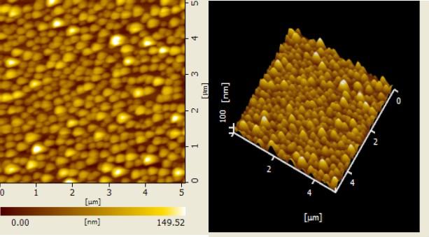
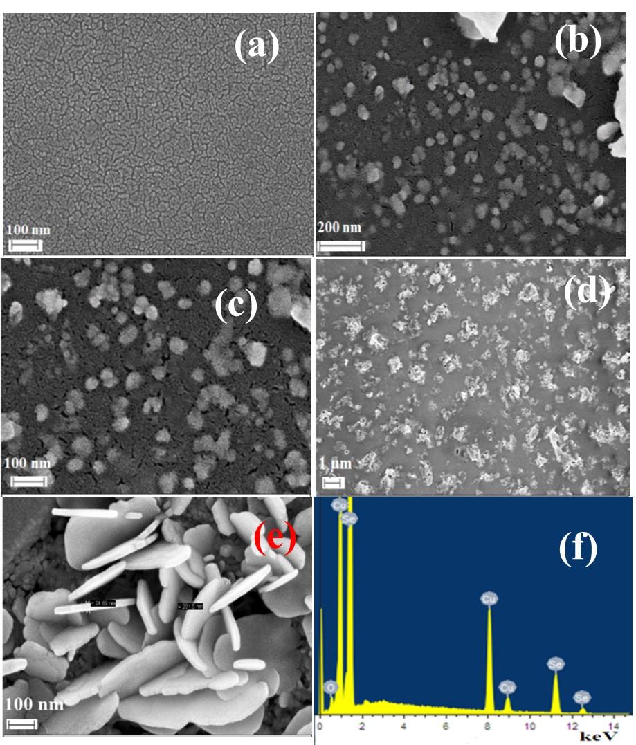
2 Whereh, k, l are the miller indices for corresponding planes. Crystallite sizes and lattice parameters at various temperatures are presented in the table 1. We observed that crystallite size is increasing with annealing temperature. Cu, Se powders were taken in Cu: Se (1:1) ratio and thoroughly grinded for 30 min by mechano-chemical method. We tested it with the formation of CuSe(figure 3.2.) by comparing the peaks with the standard data (JCPDS ) and found to be in hexagonal phase. Also, we made a pellet for resistivity measurement, which is also showing the CuSe formation shown in the fig Optical properties The absorption spectra of copper selenide thin films of as-deposited and annealed at various temperatures (200 0 C, C, C and C) were shown in the fig 4. We observed that there is a decrease in the intensity of absorption spectra of annealed films. The absorption spectra are temperature independent, confirming that CuSe thin films show direct transition. A blue shift of absorption spectrum is observed with increase in annealing temperature, indicating that band gap increase with annealing temperature. The thickness and band gaps of as-deposited and annealed CuSe thin films are presented in the table 2. Variation of thickness and band gap of as-deposited and annealed CuSe thin films with temperature is shown in fig 5. The thickness of the CuSe thin films is decreasing with temperature whereas band gap increases with annealing temperature, confirming the blue shift of absorption spectra shown in fig4. Because of the crystallinity and higher transparency, the Copper selenide films are suitable for optical analysis from which the absorption coefficient and energy band gap may be determined. In the fundamental absorption region the optical absorption coefficient, α was evaluated using the relation, α = (lna -1 )/t, where t is the film thickness and A is the absorbance. The best linear relationship is obtained by plotting α 1/2 against hν, based on the below equation, αhν = A (hν Eg) n/2 Where, α is absorption coefficient, A is constant (independent of ν) and n is the exponent that depends on the quantum selection rules for the particular material. The photon energy (hν) for x-axis can be calculated using below equqtion, E = hν = hc/λ Where, h is Planck s constant (6.626x10⁻³⁴ Js), c is speed of light (3x10 8 m/s) and λ is the wavelength of the light used.with increase in the annealing temperature, the thickness of the film was decreasing. However, the corresponding band gap was increasing with temperature. The same was presented in the fig Surface analysis The morphology of the films was substantially affected by the annealing temperature. The as-deposited film, without annealing, has a rough surface and irregular grain size as observed in fig6a. When the films were annealed at 200 C for 30 minutes, the morphology was not changed much but showed better uniformity in grain size (fig 6 b). The annealed film at 300 C shows a continuous and homogeneous granular surface as observed in fig6c. The morphology showed dense spherical structures and no visible defects indicate that the films are completely covered with particles. And figures 6 d, 6 e and 6 f are clearly shows the particle size was increased with annealing temperature. The grain sizes and RMS roughness of as such and annealed films were shown in the table 3. The random distribution of grains, in projection and size, only suggests a random nucleation mechanism and random orientation of grains show that the grain growth is isotropic. The dependence of grain size, RMS roughness on temperature is demonstrated in the figure 7. The grain size increased more rapidly with the annealing temperature and the grain growth rate increases more rapidly at higher annealing temperature. This kinetics of grain growth trend was influenced by the grain size which is in agreement with Huda and Ralph [1]. 3.4 FESEM Figure 8a shows FESEM image of as deposited CuSe film deposited on borosilicate glass substrate and annealed at 200 C, 500 C for 30 minutes. It can be clearly seen that the copper selenide surface is smooth and high dense with uniform cracks. The crystal grains of the copper selenide film are uniformly distributed on the surface and grain size is about nm, indicating that the copper selenide film has a well-defined surface morphology. The figures, 8 b and 8c show the morphology and the fully spherical nanoparticles with well separation in Copper selenide films annealed at 200 C and 500 C for 30 minutes. In XRD, optical results clearly agree with this morphological changes. In case of Figure 8 d the partially cover with flakes type morphology with high porosity happen in the films due to the annealing effect at 500 C. But in case of pellet form, a beautiful disk type micro structure has seen in figure 8e. The Electron dispersive scattering (EDS) spectrum in figure 8f clearly shows the elemental analysis of CuSe formation with high purity with 1:1 stoichiometry ratio. 66 Page
3 3.5 Resistivity and Figure of Merit (ZT) The temperature dependence of resistivity is shown in figure 3.9. The resistivity of copper selenide increases with temperature and at room temperature (300K), resistivity is measured as μωm. Due to various reasons, we could not measure Seebeck coefficient and thermal conductivity of the sample. However, to get a feel we have taken the above said values from literature[9] to calculate figure of merit of the sample. At room temperature (300K), the Seebeck coefficient and thermal conductivity values are taken as 75 μv//k and 0.4 Wm -1 K -1 respectively. Hence, figure of merit is calculated as 1.34 at 300 K. Also, the emphasis has to be made in preparing nano particles, which greatly reduces the thermal conductivity, thereby increasing the figure of merit. The Cu x Se 1-x stoichiometry ratios for improved figure of merit is under investigation. IV. Conclusions XRD and AFM studies show that the crystallite size of Copper Selenide increases with temperature and spectroscopic studies tell that the band gap increases with the annealing temperature. The high band gap materials are employed in high temperature applications. The figure of merit for the sample is calculated as 1.34 at 300 K, which is high compared to other thermoelectric materials. Acknowledgement: DR & RRC thanks to School of Physics - University of Hyderabad for providing goodexperimental facilities. DR specially thanks to UGC-BSR for financial support. References: [1] M. S. Dresselhaus, G. Chen, M. Y. Tang, R. G.Yang, H. Lee, D. Z. Wang, Z. Ren, J. P. Fleurial, P. Gogna,Adv.Mater.2007,19, 1043; [2] F. J. DiSalvo, Science1999, 285, 703; [3] J. R. Sootsman, D. Y. Chung, M. G. Kanatzidis,Angew. Chem.2009, 121, 8768; Angew. Chem. Int. Ed.2009, 48, 8616 [4] W.X. Zhang, X.M. Zhang, L. Zhang, J.X. Wu, Z.H. Hui,Y.W. Cheng,J.W. Liu, Y. Xie, and Y.T. Qian, Inorg.Chem. 39 (2000)1838. [5] W. Z. Wang, P. Yan,F.Y. Liu, Y. Xie, Y. Geng and Y.T. Qian, J. Mater.Chem. 8 (1998)2321. [6] Z.P. Qiao, Y. Xie, J.G. Xu, X.M. Liu, Y.J. Zhu and Y.T. Qian, Can.J.Chem. 78 (2000)1143. [7] J.J. Zhu, O.Palchik, S.G. Chen and A. Gedanken, J. Phys.Chem. B 104 (2000)7344. [8] Hong-Liang Li et al., J. Mat. Che. 12 (2002) [9]. B. Yu, et al., Thermoelectric properties of copper selenide with ordered selenium layer and disordered copper layer, Nano Energy, Figure Captions Fig. 1. X- raydiffractogram of as-deposited and annealed at C & C of copper selenide thin films. Fig. 2. X- raydiffractogram of Copper selenide powder Fig. 3. X- raydiffractogram of Copper selenide pellet. Fig. 4. Absorption spectra of as deposited and annealed at C, C, C & C copper selenide thin films. Fig. 5. Variation of thickness and band gap of as-deposited and annealed CuSe thin films with temperature. Fig. 6. AFM micrographs of copper selenide (a) as deposited film, and thin films annealed at (b) C and (c) C (d) C (e) C (f) 3-dimensional view of fig 6 e. Fig. 7. Variation of crystallite size and RMS roughness of surface of CuSe films with temperature. Fig. 8. FESEM micrographs of (a) as-deposited film, annealed at (b) C and (c) C (d) C copper selenide thin films (e) pellet and (f) EDS spectrum of the compound. Fig. 9.Temperature dependence of resistivity. Table Table 1. Microstructural parameters associated with the respective samples. Table 2. Thickness and band gaps of as-deposited and annealed Copper selenide thin films. Table 3. Crystallite size and RMS roughness of as-deposited and annealed films. 67 Page

4 Figures 68 Page
 (f 69")
5 Figure 6 (e) (f 69 Page
6 70 Page
7 Figure 8 List of Tables Crystallite Size Lattice parameters (nm) SAMPLE\ MEASUREMENT (nm) Powder a = 1.420, c = Pellet a = 1.414, c = As-deposited Thin Film Annealed at C Annealed at C a = 1.415, c = Table 1 Annealing Temperature ( 0 C) Thickness (nm) Band Gap (ev) As deposited film Table 2 SAMPLE \ MEASUREMENT Crystallite size (nanometres) RMS roughness (nanometres) As-deposited film Annealed at C Annealed at C Annealed at C Annealed at C Table 3 71 Page
Applications of Successive Ionic Layer Adsorption and Reaction (SILAR) Technique for CZTS Thin Film Solar Cells
 Technique for CZTS Thin Film Solar Cells") NANO VISION An International Open Free Access, Peer Reviewed Research Journal www.nano-journal.org ISSN 2231-2579 (Print) ISSN 2319-7633 (Online) Abbr: Nano Vision. 2013, Vol.3(3): Pg.235-239 Applications
NANO VISION An International Open Free Access, Peer Reviewed Research Journal www.nano-journal.org ISSN 2231-2579 (Print) ISSN 2319-7633 (Online) Abbr: Nano Vision. 2013, Vol.3(3): Pg.235-239 Applications
Growth Of TiO 2 Films By RF Magnetron Sputtering Studies On The Structural And Optical Properties
 Journal of Multidisciplinary Engineering Science and Technology (JMEST) Growth Of TiO 2 Films By RF Magnetron Sputtering Studies On The Structural And Optical Properties Ahmed K. Abbas 1, Mohammed K. Khalaf
Structural, Optical and Surface Properties of CdTe Thin Films on CdS/FTO Glass Substrates
 American Journal of Materials Science and Application 2015; 3(6): 76-80 Published online November 2, 2015 (http://www.openscienceonline.com/journal/ajmsa) Structural, Optical and Surface Properties of
Structural and Optical Properties of Aluminium Antimonide Thin Films Deposited By Thermal Evaporation Method
 Available online at www.scholarsresearchlibrary.com Scholars Research Library Archives of Physics Research, 2011, 2 (1): 146-153 (http://scholarsresearchlibrary.com/archive.html) ISSN 0976-0970 CODEN (USA):
INFLUENCE OF TiO2 THIN FILM ANNEALING TEMPERATURE ON ELECTRICAL PROPERTIES SYNTHESIZED BY CVD TECHNIQUE
 INFLUENCE OF TiO2 THIN FILM ANNEALING TEMPERATURE ON ELECTRICAL PROPERTIES SYNTHESIZED BY CVD TECHNIQUE F. N. Mohamed, M. S. A. Rahim, N. Nayan, M. K. Ahmad, M. Z. Sahdan and J. Lias Faculty of Electrical
Structural and optical characterization of reactive evaporated tin diselenide thin films
 IOP Conference Series: Materials Science and Engineering OPEN ACCESS Structural and optical characterization of reactive evaporated tin diselenide thin films Recent citations - Studies on Physical Properties
SYNTHESIS, CHARACTERIZATION AND PHOTOCATALYTIC ACTIVITY OF MgO NANOPARTICLES
 SYNTHESIS, CHARACTERIZATION AND PHOTOCATALYTIC ACTIVITY OF MgO NANOPARTICLES Bhagya J 1,2, Dedhila Devadathan 1, Baiju V 1, Biju R 1, Raveendran R 1 1 Nanoscience Research Laboratory, Department of Physics,
EFFECT OF AIR ANNEALING ON CuSbS 2 THIN FILM GROWN BY VACUUM THERMAL EVAPORATION
 Chalcogenide Letters Vol. 8, No. 4, April 2011, p. 255-262 EFFECT OF AIR ANNEALING ON CuSbS 2 THIN FILM GROWN BY VACUUM THERMAL EVAPORATION A. RABHI *, M. KANZARI Laboratoire de Photovoltaïque et Matériaux
EFFECT OF DEPOSITION TIME ON CHEMICAL BATH DEPOSITION PROCESS AND THICKNESS OF BaSe THIN FILMS.
 Journal of Optoelectronics and Biomedical Materials Vol. 3 Issue 4, October-December 2011 p. 81-85 EFFECT OF DEPOSITION TIME ON CHEMICAL BATH DEPOSITION PROCESS AND THICKNESS OF BaSe THIN FILMS. N.A. OKEREKE
Structural and Optical Properties of MnO 2 : Pb Nanocrystalline Thin Films Deposited By Chemical Spray Pyrolysis
 IOSR Journal of Engineering (IOSRJEN) e-issn: 2250-3021, p-issn: 2278-8719 Vol. 3, Issue 4 (April. 2013), V4 PP 52-57 Structural and Optical Properties of MnO 2 : Pb Nanocrystalline Thin Films Deposited
Visual and Surface Properties of CdTe Thin Films on CdS/FTO Glass Substrates
 International Journal of Electrical and Computer Engineering (IJECE) Vol. 6, No. 2, April 2016, pp. 468~473 ISSN: 2088-8708, DOI: 10.11591/ijece.v6i2.9064 468 Visual and Surface Properties of CdTe Thin
High Resolution X-ray Diffraction
 High Resolution X-ray Diffraction Nina Heinig with data from Dr. Zhihao Donovan Chen, Panalytical and slides from Colorado State University Outline Watlab s new tool: Panalytical MRD system Techniques:
for New Energy Materials and Devices; Beijing National Laboratory for Condense Matter Physics,
 Electronic Supplementary Information Highly efficient core shell CuInS 2 /Mn doped CdS quantum dots sensitized solar cells Jianheng Luo, a Huiyun Wei, a Qingli Huang, a Xing Hu, a Haofei Zhao, b Richeng
Thermal Annealing Effects on the Thermoelectric and Optical Properties of SiO 2 /SiO 2 +Au Multilayer Thin Films
 American Journal of Materials Science 2015, 5(3A): 31-35 DOI: 10.5923/s.materials.201502.05 Thermal Annealing Effects on the Thermoelectric and Optical Properties of SiO 2 /SiO 2 +Au Multilayer Thin Films
Structural and optical properties of electron beam evaporated CdSe thin films
 Bull. Mater. Sci., Vol. 30, No. 6, December 2007, pp. 547 551. Indian Academy of Sciences. Structural and optical properties of electron beam evaporated CdSe thin films N J SUTHAN KISSINGER*, M JAYACHANDRAN
X ray diffraction in materials science
 X ray diffraction in materials science Goals: Use XRD spectra to determine the orientation of single crystals and preferred orientations in a thin film. Understand how grain size and strain affect the
Ultrathin Nanosheets of Feroxyhyte: A New Two-dimensional. Hefei National Laboratory for Physical Sciences at Microscale,
 Electronic Supplementary Material (ESI) for Chemical Science. This journal is The Royal Society of Chemistry 2014 Electronic Supplementary Information for Ultrathin Nanosheets of Feroxyhyte: A New Two-dimensional
Structural and optical properties of CuO thin films prepared via R.F.magnetron sputtering
 Structural and optical properties of CuO thin films prepared via R.F.magnetron sputtering Riyam A. Hammoodi 1, Assist. Prof.Dr.Ahmed K. Abbas 1 and Prof. Dr.Abdulhussein K.Elttayef 2 1 University of Wasit,
Mn DOPED SnO2 Semiconducting Magnetic Thin Films Prepared by Spray Pyrolysis Method
 International Journal of Scientific & Engineering Research Volume 2, Issue 4, April-2011 1 Mn DOPED SnO2 Semiconducting Magnetic Thin Films Prepared by Spray Pyrolysis Method K.Vadivel, V.Arivazhagan,
Structure and optical properties of M/ZnO (M=Au, Cu, Pt) nanocomposites
 nanocomposites") Solar Energy Materials & Solar Cells 8 () 339 38 Structure and optical properties of M/ (M=Au, Cu, Pt) nanocomposites U. Pal a,b, *, J. Garc!ıa-Serrano a, G. Casarrubias-Segura a, N. Koshizaki c, T. Sasaki
Solar Energy Materials & Solar Cells 8 () 339 38 Structure and optical properties of M/ (M=Au, Cu, Pt) nanocomposites U. Pal a,b, *, J. Garc!ıa-Serrano a, G. Casarrubias-Segura a, N. Koshizaki c, T. Sasaki
Supplementary Information
 Supplementary Information Formation of oxygen vacancies and Ti 3+ state in TiO 2 thin film and enhanced optical properties by air plasma treatment Bandna Bharti a, Santosh Kumar b, Heung-No Lee c and Rajesh
Supporting Information
 Supporting Information Controlled Vapor Phase Growth of Single Crystalline, Two-Dimensional GaSe Crystals with High Photoresponse Xufan Li, Ming-Wei Lin, Alexander A. Puretzky, Juan C. Idrobo, Cheng Ma,
Preparation and characterization of nanostructured thermoelectric materials
 QuickTime et un décompresseur TIFF (non compressé) sont requis pour visionner cette image. Preparation and characterization of nanostructured thermoelectric materials Laboratoire de Physique des Matériaux,
INFLUENCE OF THE [Cu]/[In] RATIO ON THE PROPERTIES OF CuInSe 2 THIN FILMS
![INFLUENCE OF THE [Cu]/[In] RATIO ON THE PROPERTIES OF CuInSe 2 THIN FILMS](/thumbs/72/67551213.jpg "INFLUENCE OF THE [Cu]/[In] RATIO ON THE PROPERTIES OF CuInSe 2 THIN FILMS") Chalcogenide Letters Vol. 11, No. 11, November 2014, p. 605-610 INFLUENCE OF THE [Cu]/[In] RATIO ON THE PROPERTIES OF CuInSe 2 THIN FILMS FIANTI, KYOO HO KIM * School of Materials Science and Engineering,
Chalcogenide Letters Vol. 11, No. 11, November 2014, p. 605-610 INFLUENCE OF THE [Cu]/[In] RATIO ON THE PROPERTIES OF CuInSe 2 THIN FILMS FIANTI, KYOO HO KIM * School of Materials Science and Engineering,
Structural and Optical Properties of SnS Thin Films
 J. Nano. Adv. Mat., No., 43-49 (4) 43 Structural and Optical Properties of SnS Thin Films Bushra A. Hasan, * and Ikhlas H. Shallal Journal of Nanotechnology & Advanced Materials An International Journal
Preparation and structural characterization of thin-film CdTe/CdS heterojunctions
 JOURNAL OF OPTOELECTRONICS AND ADVANCED MATERIALS Vol. 8, No., June 006, p. 96-940 Preparation and structural characterization of thin-film CdTe/ heterojunctions I. SALAORU a, P. A. BUFFAT b, D. LAUB b,
International Journal of Engineering & Technology IJET-IJENS Vol:14 No:01 88
 International Journal of Engineering & Technology IJET-IJENS Vol:14 No:01 88 Effect of Temperature On Ba (1-x) Sr x Fe 11.4 Ti (0.3) Mn (0.3) O 19 (x = 0.3, 0.7) Against Crystallite Size Characterization
Iron oxide(iii) nanoparticles fabricated by electron beam irradiation method
 nanoparticles fabricated by electron beam irradiation method") Materials Science-Poland, Vol. 25, No. 4, 2007 Iron oxide(iii) nanoparticles fabricated by electron beam irradiation method B. ZHAO 1, Y. WANG 1, H. GUO 1, J. WANG 2, Y. HE 2, Z. JIAO 1*, M. WU 2 1 Institute
Materials Science-Poland, Vol. 25, No. 4, 2007 Iron oxide(iii) nanoparticles fabricated by electron beam irradiation method B. ZHAO 1, Y. WANG 1, H. GUO 1, J. WANG 2, Y. HE 2, Z. JIAO 1*, M. WU 2 1 Institute
Influence of Thermal Annealing on the Structural and Optical Properties of Lead Oxide Thin Films Prepared by Chemical Bath Deposition Technique
 Influence of Thermal Annealing on the Structural and Optical Properties of Lead Oxide Thin Films Prepared by Chemical Bath Deposition Technique D.D.O. Eya, Ph.D. Department of Physics, Federal University
This journal is The Royal Society of Chemistry S 1
 2013 S 1 Thermochemical analysis on the growth of NiAl 2 O 4 rods Sang Sub Kim, a Yong Jung Kwon, b Gunju Sun, a Hyoun Woo Kim,* b and Ping Wu* c a Department of Materials Science and Engineering, Inha
Cu(In,Ga)Se 2 FILM FORMATION FROM SELENIZATION OF MIXED METAL/METAL-SELENIDE PRECURSORS
Se 2 FILM FORMATION FROM SELENIZATION OF MIXED METAL/METAL-SELENIDE PRECURSORS") Cu(In,Ga)Se 2 FILM FORMATION FROM SELENIZATION OF MIX METAL/METAL-SELENIDE PRECURSORS Rui Kamada, William N. Shafarman, and Robert W. Birkmire Institute of Energy Conversion University of Delaware, Newark,
Cu(In,Ga)Se 2 FILM FORMATION FROM SELENIZATION OF MIX METAL/METAL-SELENIDE PRECURSORS Rui Kamada, William N. Shafarman, and Robert W. Birkmire Institute of Energy Conversion University of Delaware, Newark,
High Transmittance Ti doped ITO Transparent Conducting Layer Applying to UV-LED. Y. H. Lin and C. Y. Liu
 High Transmittance Ti doped ITO Transparent Conducting Layer Applying to UV-LED Y. H. Lin and C. Y. Liu Department of Chemical Engineering and Materials Engineering, National Central University, Jhongli,
Thin Film Characterizations Using XRD The Cases of VO2 and NbTiN
 Thin Film Characterizations Using XRD The Cases of VO2 and NbTiN A thesis submitted in partial fulfillment of the requirement for the degree of Bachelor of Arts / Science in Physics from The College of
Synthesis of Y 2 O 3 Nanoparticles by Modified Transient Morphology Method
 2011 International Conference on Chemistry and Chemical Process IPCBEE vol.10 (2011) (2011) IACSIT Press, Singapore Synthesis of Y 2 O 3 Nanoparticles by Modified Transient Morphology Method Zobadeh Momeni
Solid-state thermoelectric (TE) converters are recently
 converters are recently") Experimental Studies on Anisotropic Thermoelectric Properties and Structures of n-type Bi 2 Te 2.7 Se 0.3 Xiao Yan, Bed Poudel, Yi Ma, W. S. Liu, G. Joshi, Hui Wang, Yucheng Lan, Dezhi Wang, Gang Chen,*,
Experimental Studies on Anisotropic Thermoelectric Properties and Structures of n-type Bi 2 Te 2.7 Se 0.3 Xiao Yan, Bed Poudel, Yi Ma, W. S. Liu, G. Joshi, Hui Wang, Yucheng Lan, Dezhi Wang, Gang Chen,*,
Structural, optical and electrical properties of chemically deposited copper selenide films
 Bull. Mater. Sci., Vol. 32, No. 1, February 2009, pp. 37 42. Indian Academy of Sciences. Structural, optical and electrical properties of chemically deposited copper selenide films R H BARI, V GANESAN,
INVESTIGATION OF NANOCRYSTALS USING TEM MICROGRAPHS AND ELECTRON DIFFRACTION TECHNIQUE
 INVESTIGATION OF NANOCRYSTALS USING TEM MICROGRAPHS AND ELECTRON DIFFRACTION TECHNIQUE CAMELIA OPREA, VICTOR CIUPINA, GABRIEL PRODAN Department of Physics, Ovidius University, Constanþa, 900527, Romania
An Analysis of Structural and Optical Properties Undoped ZnS and Doped (with Mn, Ni) ZnS Nano Particles
 ZnS Nano Particles") Journal of Modern Physics, 213, 4, 122-126 http://dx.doi.org/1.4236/jmp.213.47137 Published Online July 213 (http://www.scirp.org/journal/jmp) An Analysis of Structural and Optical Properties Undoped ZnS
Journal of Modern Physics, 213, 4, 122-126 http://dx.doi.org/1.4236/jmp.213.47137 Published Online July 213 (http://www.scirp.org/journal/jmp) An Analysis of Structural and Optical Properties Undoped ZnS
Effects of Annealing Treatment on Optical Properties of Anatase TiO 2 Thin Films
 Effects of Annealing Treatment on Optical Properties of Anatase TiO Thin Films M. M. Hasan, A. S. M. A. Haseeb, R. Saidur, and H. H. Masjuki Abstract In this investigation, anatase TiO thin films were
Growth and Doping of SiC-Thin Films on Low-Stress, Amorphous Si 3 N 4 /Si Substrates for Robust Microelectromechanical Systems Applications
 Journal of ELECTRONIC MATERIALS, Vol. 31, No. 5, 2002 Special Issue Paper Growth and Doping of SiC-Thin Films on Low-Stress, Amorphous Si 3 N 4 /Si Substrates for Robust Microelectromechanical Systems
ZnO-based Transparent Conductive Oxide Thin Films
 IEEE EDS Mini-colloquium WIMNACT 32 ZnO-based Transparent Conductive Oxide Thin Films Weijie SONG Ningbo Institute of Material Technology and Engineering, Chinese Academy of Sciences, Ningbo, P. R. China
Supporting Online Material for
 www.sciencemag.org/cgi/content/full/science.1200448/dc1 Supporting Online Material for Increasing Solar Absorption for Photocatalysis with Black Hydrogenated Titanium Dioxide Nanocrystals This PDF file
Microstructural Evolution of Ti-Mo-Ni-C Powder by Mechanical Alloying
 Materials Transactions, Vol. 50, No. 1 (2009) pp. 117 to 122 #2009 The Japan Institute of Metals Microstructural Evolution of -Mo-Ni-C Powder by Mechanical Alloying Hiroyuki Hosokawa, Kiyotaka Kato, Koji
Deposition and Characterization of p-cu 2 O Thin Films
 SUST Journal of Science and Technology, Vol., No. 6, 1; P:1-7 Deposition and Characterization of p- O Thin Films (Submitted: July 18, 1; Accepted for Publication: November 9, 1) M. Rasadujjaman 1*, M.
"OPTICAL AND ELECTRICAL PROPERTIES OF ZnTe AND ZnTe:O THIN FILMS DEPOSITED BY CSVT TECHNIQUE"
 "OPTICAL AND ELECTRICAL PROPERTIES OF ZnTe AND ZnTe:O THIN FILMS DEPOSITED BY CSVT TECHNIQUE" M. A. González Trujillo 1, M.L. Albor Aguilera 2 D.A. Rodríguez Morán 3 M. Galván Arellano 4, A. Morales Acevedo
Available online at ScienceDirect. Materials Today: Proceedings 2 (2015 )
") Available online at www.sciencedirect.com ScienceDirect Materials Today: Proceedings 2 (2015 ) 5582 5586 International Conference on Solid State Physics 2013 (ICSSP 13) Thickness dependent optimization
Available online at www.sciencedirect.com ScienceDirect Materials Today: Proceedings 2 (2015 ) 5582 5586 International Conference on Solid State Physics 2013 (ICSSP 13) Thickness dependent optimization
Diffraction: Powder Method
 Diffraction: Powder Method Diffraction Methods Diffraction can occur whenever Bragg s law λ = d sin θ is satisfied. With monochromatic x-rays and arbitrary setting of a single crystal in a beam generally
It is instructive however for you to do a simple structure by hand. Rocksalt Structure. Quite common in nature. KCl, NaCl, MgO
 Today the structure determinations etc are all computer -assisted It is instructive however for you to do a simple structure by hand Rocksalt Structure Quite common in nature KCl, NaCl, MgO 9-1 Typical
LOT. Contents. Introduction to Thin Film Technology. Chair of Surface and Materials Technology
 Introduction to Thin Film Contents 1. Introduction and Application Examples (2h) 2. Preparation of Thin Films by PVD (Physical Vapor Deposition) (6h) 2.1 Vacuum Technique (1h) 2.1.1 Kinetics of Gases 2.1.2
IJRASET: All Rights are Reserved
 Physical Properties of Nanocrystalline Tin Oxide Thin Film by Chemical Spray Pyrolysis Method M. Karunakaran 1, S. Maheswari 2, K.Kasirajan 3, S. Dineshraj 4 1,3,4 Department of Physics, Alagappa Government
Mater. Res. Soc. Symp. Proc. Vol Materials Research Society
 Mater. Res. Soc. Symp. Proc. Vol. 940 2006 Materials Research Society 0940-P13-12 A Novel Fabrication Technique for Developing Metal Nanodroplet Arrays Christopher Edgar, Chad Johns, and M. Saif Islam
GROWTH, OPTICAL AND STRUCTURAL CHARACTERIZATION OF SEMI ORGANIC NON LINEAR OPTICAL THIOSEMICARBAZIDE BORATE (TSCB) SINGLE CRYSTALS
 SINGLE CRYSTALS") Indian Journal of Pure and Applied Physics (IJPAP) Vol.1.No.1 2013 pp 7-11 available at: www.goniv.com Paper Received :10-04-2013 Paper Published:26-04-2013 Paper Reviewed by: 1. Dr.S.Selvakumar 2. Hendry
Indian Journal of Pure and Applied Physics (IJPAP) Vol.1.No.1 2013 pp 7-11 available at: www.goniv.com Paper Received :10-04-2013 Paper Published:26-04-2013 Paper Reviewed by: 1. Dr.S.Selvakumar 2. Hendry
RightCopyright 2006 American Vacuum Soci
 Title Gallium nitride thin films deposite magnetron sputtering Author(s) Maruyama, T; Miyake, H Citation JOURNAL OF VACUUM SCIENCE & (2006), 24(4): 1096-1099 TECHNOL Issue Date 2006 URL http://hdl.handle.net/2433/43541
Journal of Chemical and Pharmaceutical Research, 2017, 9(1): Research Article
: Research Article") Available online www.jocpr.com Journal of Chemical and Pharmaceutical Research, 2017, 9(1):163-167 Research Article ISSN : 0975-7384 CODEN(USA) : JCPRC5 Synthesis and Characterization of Carbon Nano Spheres
Available online www.jocpr.com Journal of Chemical and Pharmaceutical Research, 2017, 9(1):163-167 Research Article ISSN : 0975-7384 CODEN(USA) : JCPRC5 Synthesis and Characterization of Carbon Nano Spheres
Enhanced Thermal Conductivity of Polyimide Films via a Hybrid of Micro- and Nano-Sized Boron Nitride
 The 2012 World Congress on Advances in Civil, Environmental, and Materials Research (ACEM 12) Seoul, Korea, August 26-30, 2012 Enhanced Thermal Conductivity of Polyimide Films via a Hybrid of Micro- and
Supplementary Figure 1 Scanning electron micrograph (SEM) of a groove-structured silicon substrate. The micropillars are ca. 10 μm wide, 20 μm high
 of a groove-structured silicon substrate. The micropillars are ca. 10 μm wide, 20 μm high") Supplementary Figure 1 Scanning electron micrograph (SEM) of a groove-structured silicon substrate. The micropillars are ca. 10 μm wide, 20 μm high and own the gap of 10 μm. Supplementary Figure 2 Strictly
Supplementary Figure 1 Scanning electron micrograph (SEM) of a groove-structured silicon substrate. The micropillars are ca. 10 μm wide, 20 μm high and own the gap of 10 μm. Supplementary Figure 2 Strictly
A NOVEL METHOD FOR THE IMPROVEMENT IN THERMOELECTRIC PROPERTY OF TIN OXIDE THIN FILMS AND ITS APPLICATION IN GAS SENSING
 INTERNATIONAL JOURNAL ON SMART SENSING AND INTELLIGENT SYSTEMS, VOL. 1, NO. 2, JUNE 2008 A NOVEL METHOD FOR THE IMPROVEMENT IN THERMOELECTRIC PROPERTY OF TIN OXIDE THIN FILMS AND ITS APPLICATION IN GAS
INFLUENCE OF THICKNESS VARIATION ON THE OPTICAL PROPERTIES OF ZnO THIN FILMS PREPARED BY THERMAL EVAPORATION METHOD
 Journal of Electron Devices, Vol. 0, 20, pp. 448-455 JED [ISSN: 682-3427 ] INFLUENCE OF THICKNESS VARIATION ON THE OPTICAL PROPERTIES OF ZnO THIN FILMS PREPARED BY THERMAL EVAPORATION METHOD Farzana Chowdhury
Characterization of Cadmium Tin Oxide Thin Films as a Window Layer for Solar Cell
 Characterization of Cadmium Tin Oxide Thin Films as a Window Layer for Solar Cell ABSTRACT Cadmium tin oxide thin (Cd 2SnO 4 ) films prepared by thermal evaporation technique at room temperature. The film
Deposition-Temperature Effects on AZO Thin Films Prepared by RF Magnetron Sputtering and Their Physical Properties
 Journal of the Korean Physical Society, Vol. 49, December 2006, pp. S584 S588 Deposition-Temperature Effects on AZO Thin Films Prepared by RF Magnetron Sputtering and Their Physical Properties Jeung Hun
Steric Effects on the. Transition in YH x
 Steric Effects on the Metallic-Mirror Mirror to Transparent-Insulator Transition in YH x Troy C. Messina Department of Physics University of Texas at Austin Final Defense 22 November 2002 Outline Introduction
Romanian Academy Institute of Physical Chemistry Ilie Murgulescu. PhD THESIS SUMMARY
 Romanian Academy Institute of Physical Chemistry Ilie Murgulescu PhD THESIS SUMMARY CORRELATIONS BETWEEN STRUCTURAL AND PHYSICO - CHEMICAL PROPERTIES OF THE SEMICONDUCTOR OXIDES WITH OPTIC, SENSORISTIC
Research Article Optical and Electrical Properties of Ag-Doped In 2 S 3 Thin Films Prepared by Thermal Evaporation
 Advances in Materials Science and Engineering, Article ID 37861, 4 pages http://dx.doi.org/1.1155/214/37861 Research Article Optical and Electrical Properties of Ag-Doped In 2 S 3 Thin Films Prepared by
Study of structural property of n-type indium antimonide thin films
 Indian Journal of Pure & Applied Physics Vol. 5, May 212, pp. 339-346 Study of structural property of n-type indium antimonide thin films S R Vishwakarma*, A K Verma, R S N Tripathi, S Das & Rahul Department
Silver Diffusion Bonding and Layer Transfer of Lithium Niobate to Silicon
 Chapter 5 Silver Diffusion Bonding and Layer Transfer of Lithium Niobate to Silicon 5.1 Introduction In this chapter, we discuss a method of metallic bonding between two deposited silver layers. A diffusion
Supporting Information
 Copyright WILEY-VCH Verlag GmbH & Co. KGaA, 69469 Weinheim, Germany, 2013. Supporting Information for Adv. Funct. Mater., DOI: 10.1002/adfm.201302405 Self-Assembly Mechanism of Spiky Magnetoplasmonic Supraparticles
The Effects of the Adding V2O5 on the Oxide Semiconductor Layer of a Dye-sensitized Solar Cell
 , pp.66-71 http://dx.doi.org/10.14257/astl.2016.140.14 The Effects of the Adding V2O5 on the Oxide Semiconductor Layer of a Dye-sensitized Solar Cell Don-Kyu Lee Electrical Engineering, Dong-Eui University,
Microstructures and Properties of Sintered Cu-MoS2/Cu Functional Gradient Materials Ai-Qin Wanga1,*, Ting-Ting Liangb1, Dou-Qin Mac1and Jing-Pei Xied2
 International Conference on Manufacturing Engineering and Intelligent Materials (ICMEIM 217) Microstructures and Properties of Sintered -MoS2/ Functional Gradient Materials Ai-Qin Wanga1,*, Ting-Ting Liangb1,
MICROWAVE DIELECTRIC PROPERTIES OF Ba 0.75 Sr 0.25 (Nd x Bi 1-x ) 2 Ti 4 O 12 SOLID SOLUTION
 2 Ti 4 O 12 SOLID SOLUTION") Original papers MICROWAVE DIELECTRIC PROPERTIES OF Ba 0.75 Sr 0.25 (Nd x Bi 1-x ) 2 Ti 4 O 12 SOLID SOLUTION Long Mingzhu, ZHuang WENDONG*, # Tang Bin, Yu Shengquan, Zhou Xiaohua, Zhang Shuren State Key
Original papers MICROWAVE DIELECTRIC PROPERTIES OF Ba 0.75 Sr 0.25 (Nd x Bi 1-x ) 2 Ti 4 O 12 SOLID SOLUTION Long Mingzhu, ZHuang WENDONG*, # Tang Bin, Yu Shengquan, Zhou Xiaohua, Zhang Shuren State Key
IN-SITU ANNEALING OF Cu(In,Ga)Se 2 FILMS GROWN BY ELEMENTAL CO- EVAPORATION
Se 2 FILMS GROWN BY ELEMENTAL CO- EVAPORATION") IN-SITU ANNEALING OF Cu(In,Ga)Se 2 FILMS GROWN BY ELEMENTAL CO- EVAPORATION James D. Wilson, Robert W. Birkmire, William N. Shafarman Institute of Energy Conversion, University of Delaware, Newark, DE
IN-SITU ANNEALING OF Cu(In,Ga)Se 2 FILMS GROWN BY ELEMENTAL CO- EVAPORATION James D. Wilson, Robert W. Birkmire, William N. Shafarman Institute of Energy Conversion, University of Delaware, Newark, DE
Keywords: MnZnFeTiO, XRD, SEM, EDX, Instrumental Broadening, Williamson-Hall Plot method.
 International Frontier Science Letters Online: 2014-10-01 ISSN: 2349-4484, Vol. 2, pp 40-51 doi:10.18052/www.scipress.com/ifsl.2.40 2014 SciPress Ltd., Switzerland XRD Studies on Titanium Substituted Manganese
The Effect of Deposition Rate on Electrical, Optical and Structural Properties of ITO Thin Films
 http://www.e-journals.net CODEN ECJHAO E- Chemistry Vol. 2, No. 3, pp 171-177, June 2005 The Effect of Deposition Rate on Electrical, Optical and Structural Properties of ITO Thin Films P.S.RAGHUPATHI,
Morfological and Structural Characteristics of II VI Semiconductor Thin Films (ZnTe, CdTe, ZnS)
") Morfological and Structural Characteristics of II VI Semiconductor Thin Films (ZnTe, CdTe, ZnS) D. Kurbatov, 1 V. Kosyak, 1, M. Kolesnyk, 1 A. Opanasyuk, 1 and S. Danilchenko 2 1 Sumy State University,
Morfological and Structural Characteristics of II VI Semiconductor Thin Films (ZnTe, CdTe, ZnS) D. Kurbatov, 1 V. Kosyak, 1, M. Kolesnyk, 1 A. Opanasyuk, 1 and S. Danilchenko 2 1 Sumy State University,
Condensed Matter II: Particle Size Broadening
 Condensed Matter II: Particle Size Broadening Benjamen P. Reed & Liam S. Howard IMAPS, Aberystwyth University March 19, 2014 Abstract Particles of 355µm silicon oxide(quartz)were subjected to a ball milling
Modified Scherrer Equation to Estimate More Accurately Nano-Crystallite Size Using XRD
 World Journal of Nano Science and Engineering, 2012, 2, 154-160 http://dx.doi.org/10.4236/wjnse.2012.23020 Published Online September 2012 (http://www.scirp.org/journal/wjnse) Modified Scherrer Equation
Experiment 2b X-Ray Diffraction* Optical Diffraction Experiments
 * Experiment 2b X-Ray Diffraction* Adapted from Teaching General Chemistry: A Materials Science Companion by A. B. Ellis et al.: ACS, Washington, DC (1993). Introduction Inorganic chemists, physicists,
X-RAY DIFFRACTION STUDIES ON LEAD PHTHALOCYANINE, ZINC PHTHALOCYANINE AND MAGNESIUM PHTHALOCYANINE THIN FILMS
 CHAPTER 5 X-RAY DIFFRACTION STUDIES ON LEAD PHTHALOCYANINE, ZINC PHTHALOCYANINE AND MAGNESIUM PHTHALOCYANINE THIN FILMS 5.1 Introduction The properties of phthalocyanine thin films are greatly influenced
EFFECT OF GROWTH TEMPERATURE ON THE CATALYST-FREE GROWTH OF LONG SILICON NANOWIRES USING RADIO FREQUENCY MAGNETRON SPUTTERING
 International Journal of Nanoscience Vol. 10, Nos. 1 & 2 (2011) 13 17 #.c World Scienti c Publishing Company DOI: 10.1142/S0219581X11007594 EFFECT OF GROWTH TEMPERATURE ON THE CATALYST-FREE GROWTH OF LONG
Volume 8, ISSN (Online), Published at:
, Published at:") IMPACT OF POWDERY OXIDE LAYER IN THE TITANIUM/RUTILE SYSTEM PREPARED BY OXIDATIVE CONSTRUCTING OF CERAMIC MATERIALS Sergey V. Shevtsov, Nikolay A. Alad ev, Konstantin A. Solntsev Baikov Institute of Metallurgy
IMPACT OF POWDERY OXIDE LAYER IN THE TITANIUM/RUTILE SYSTEM PREPARED BY OXIDATIVE CONSTRUCTING OF CERAMIC MATERIALS Sergey V. Shevtsov, Nikolay A. Alad ev, Konstantin A. Solntsev Baikov Institute of Metallurgy
Photonic Drying Pulsed Light as a low Temperature Sintering Process
 Photonic Drying Pulsed Light as a low Temperature Sintering Process Lou Panico Xenon Corporation W E S T E R N M I C H I G A N U N I V E R S I T Y PRESENTATION OVERVIEW What is Printed Electronics Materials
Supporting Information for Manuscript B516757D
 Supporting Information for Manuscript B516757D 1. UV-Vis absorption spectra Absorbance (a.u.) 0.4 0.2 5F 6F 7F 0.0 300 400 500 Wavelength (nm) Figure S1 UV-Vis spectra of, 5F, 6F and 7F in CHCl 3 solutions
OPTICAL PROPERTIES OF CdS/CuS & CuS/CdS HETEROJUNCTION THIN FILMS DEPOSITED BY CHEMICAL BATH DEPOSITION TECHNIQUE
 Journal of Ovonic Research Vol. 6, No. 3, June 21, p. 99 14 OPTICAL PROPERTIES OF / & / HETEROJUNCTION THIN FILMS DEPOSITED BY CHEMICAL BATH DEPOSITION TECHNIQUE F. I. EZEMA, D. D. HILE, S. C. EZUGWU *,
Anomaly of Film Porosity Dependence on Deposition Rate
 Anomaly of Film Porosity Dependence on Deposition Rate Stephen P. Stagon and Hanchen Huang* Department of Mechanical Engineering, University of Connecticut, Storrs, CT 06269 J. Kevin Baldwin and Amit Misra
Nanostructured Engineered Materials With High Magneto-optic Performance For Integrated Photonics Applications
 Edith Cowan University Research Online School of Engineering Publications 28 Nanostructured Engineered Materials With High Magneto-optic Performance For Integrated Photonics Applications Mikhail Vasiliev
A SOLVENT-FREE COMPOSITE SOLID ELECTROLYTES OF Li 2 CO 3 Al 2 O 3 SYSTEM PREPARED VIA WATER BASED SOL GEL METHOD
 18 TH INTERNATIONAL CONFERENCE ON COMPOSITE MATERIALS A SOLVENT-FREE COMPOSITE SOLID ELECTROLYTES OF Li 2 CO 3 Al 2 O 3 SYSTEM PREPARED VIA WATER BASED SOL GEL METHOD M. Sulaiman 1, *, A.A. Rahman 1, N.S.
Towards scalable fabrication of high efficiency polymer solar cells
 Towards scalable fabrication of high efficiency polymer solar cells Hui Joon Park 2*, Myung-Gyu Kang 1**, Se Hyun Ahn 3, Moon Kyu Kang 1, and L. Jay Guo 1,2,3 1 Department of Electrical Engineering and
Transparent Ceramic Yb 3+ :Lu2O3 Materials
 Contract no.: FA2386-10-1-4113 Final report for the project on: Transparent Ceramic Yb 3+ :Lu2O3 Materials Submission Date: Jan 19 th, 2012 Principal Investigator: Dr. Akio Ikesue World-Lab. Co., Ltd.
Performance at Wafer-Scale
 Supporting Information Self-Assembling VO 2 Nanonet with High Switching Performance at Wafer-Scale Jiasong Zhang, Haibo Jin*, Zhuo Chen, Maosheng Cao, Pengwan Chen, Yankun Dou, Yongjie Zhao, Jingbo Li*
Supporting Information
 Supporting Information Wiley-VCH 2007 69451 Weinheim, Germany Chemical Sharpening of Gold Nanorods: The Rod-to-Octahedron Transition Enrique Carbó-Argibay, Benito Rodríguez-González, Jessica Pacifico,
Normalized Absorption (a.u.) Energy (ev)
 Energy (ev)") Normalized Absorption (a.u.) PbS-Ag 4.4 mol% LCF Ag foil Ag 2 S 25500 25550 25600 Energy (ev) Supplementary Figure 1. Linear combination fit of 4.4% Ag-PbS with the weighted components and the residual
Normalized Absorption (a.u.) PbS-Ag 4.4 mol% LCF Ag foil Ag 2 S 25500 25550 25600 Energy (ev) Supplementary Figure 1. Linear combination fit of 4.4% Ag-PbS with the weighted components and the residual
The influence of physical and technological magnetron sputtering modes on the structure and optical properties of CdS and CdTe films
 PACS 81.05.Dz, 81.15.Cd The influence of physical and technological magnetron sputtering modes on the structure and optical properties of CdS and CdTe films G.S. Khrypunov, G.I. Kopach, M.M. Harchenko,
Cadmium Oxide Nano Particles by Sol-Gel and Vapour- Liquid-Solid Methods
 Nano Vision, Vol.1 (1), 47-53 (2011) Cadmium Oxide Nano Particles by Sol-Gel and Vapour- Liquid-Solid Methods S. SAKTHIVEL* and D. MANGALARAJ 1 *PG and Research Department of Physics, Rajah Serfoji Govt.
Supplementary Material (ESI) for Chemical Communications. Solid-state single-crystal-to-single-crystal transformation from a 2D
 for Chemical Communications. Solid-state single-crystal-to-single-crystal transformation from a 2D") Supplementary Material (ESI) for Chemical Communications Solid-state single-crystal-to-single-crystal transformation from a 2D layer to a 3D framework mediated by lattice iodine release Yuan-Chun He, a
Supplementary Material (ESI) for Chemical Communications Solid-state single-crystal-to-single-crystal transformation from a 2D layer to a 3D framework mediated by lattice iodine release Yuan-Chun He, a
The influence of the internal microstructure on the surface parameters of polycrystalline thin films
 The influence of the internal microstructure on the surface parameters of polycrystalline thin films C. Eisenmenger-Sittner and A. Bergauer Institut für Angewandte und Technische Physik, Technische Universität
Matrix-free synthesis of spin crossover micro-rods showing large hysteresis loop. centered at room temperature
 Electronic Supplementary Material (ESI) for ChemComm. This journal is The Royal Society of Chemistry 2015 Matrix-free synthesis of spin crossover micro-rods showing large hysteresis loop centered at room
Supplementary information. performance Li-ion battery
 Supplementary information The investigation of Ni(OH) 2 /Ni as anode for high performance Li-ion battery Shibing Ni a, Xiaohu Lv a, Tao Li a, Xuelin Yang a,and Lulu Zhang a College of Mechanical and Material
EFFECT OF MANGANESE SUBSTITUTION ON Co Ga AND Co Tl FERRITE NANOPARTICLES PREPARED BY HYDROTHERMAL ROUTE
 EFFECT OF MANGANESE SUBSTITUTION ON Co Ga AND Co Tl FERRITE NANOPARTICLES PREPARED BY HYDROTHERMAL ROUTE Gayathri.S 1, Kalainathan.S 2 1,2 Center for Crystal Growth, VIT University, Vellore - 14, Tamil
SUPPLEMENTARY INFORMATION
 In the format provided by the authors and unedited. ARTICLE NUMBER: 16178 DOI: 10.1038/NENERGY.2016.178 Enhanced Stability and Efficiency in Hole-Transport Layer Free CsSnI3 Perovskite Photovoltaics Supplementary
EFFECT AMBIENT OXIDATION ON STRUCTURAL AND OPTICAL PROPERTIES OF COPPER OXIDE THIN FILMS
 EFFECT AMBIENT OXIDATION ON STRUCTURAL AND OPTICAL PROPERTIES OF COPPER OXIDE THIN FILMS Bushra. K.H.al-Maiyaly, I.H.Khudayer 1, Ayser.J.Ibraheim 1 Associate Professor, Department of Physics, College of
Combinatorial RF Magnetron Sputtering for Rapid Materials Discovery: Methodology and Applications
 Combinatorial RF Magnetron Sputtering for Rapid Materials Discovery: Methodology and Applications Philip D. Rack,, Jason D. Fowlkes, and Yuepeng Deng Department of Materials Science and Engineering University