Investigaciones Científicas y Técnicas, Av. Bustillo 9500, 8400 San Carlos de Bariloche, Argentina.
|
|
|
- Scot Austin
- 5 years ago
- Views:
Transcription
1 1 Synthesis of nanocrystalline δ-mon by thermal annealing of amorphous thin films grown on (100) Si by reactive sputtering at room temperature N. Haberkorn, 1,2 S. Bengio, 1 H. Troiani, 1,2 S. Suárez, 1,2 P. D. Pérez, 1 M. Sirena, 1,2 J. Guimpel. 1,2 1 Centro Atómico Bariloche, Comision Nacional de Energía Atómica, Consejo Nacional de Investigaciones Científicas y Técnicas, Av. Bustillo 9500, 8400 San Carlos de Bariloche, Argentina. 2 Instituto Balseiro, Universidad Nacional de Cuyo, Comision Nacional de Energía Atómica, Av. Bustillo 9500, 8400 San Carlos de Bariloche, Argentina We report on the synthesis and characterization of nanocrystalline δ-mon by crystallization of amorphous thin films grown on (100) Si by reactive sputtering at room temperature. Films with chemical composition MoN were grown using a deposition pressure of 5mTorr with a reactive mixture of Ar/(Ar+N 2 )=0.5. The as-grown films display mostly amorphous structure. Nanocrystalline δ-mon phase is obtained after annealing at temperatures above 600 C. The superconducting critical temperature T c depends on film thickness. Thick films (170 nm) annealed at 700 C for 30 min display a T c = 11.2 K (close to the one reported for bulk specimens: 13 K), which is gradually suppressed to 7.2 K for 40 nm thick δ-mon films. Our results provide a simple method to synthesize superconducting nitride thin films on silicon wafers with T c above the ones observed for conventional superconductors such as Nb.
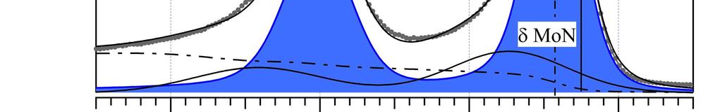
2 2 1. Introduction The synthesis of superconducting transition-metal nitrides is of technological relevance in the design of devices such as tunnel junctions [1] and electromagnetic radiation detectors [2,3]. The molybdenum nitrides present several superconducting crystalline phases: γ-mo 2 N (cubic) with T c ~ 5 K [4], β-mo 2 N (tetragonal) with superconducting critical temperature T c ~ 5 K [5] and δ-mon (hexagonal) with T c ~ 13 K [6,7]. Thin films of the different crystalline structures have been sintered through chemical and physical routes [8,9,10,11,12,13]. An outstanding feature for γ-mo 2 N and δ-mon is that sharp superconducting transitions have been observed for epitaxial and polycrystalline thin films [14,15,16]. Moreover, superconductivity has been observed for films with thicknesses of a few nanometers [14,15,17]. Recently, we have reported that the chemical concentration and T c for Mo-N thin films grown at room temperature by reactive sputtering can be modified by changing the Ar:N 2 ratio [18]. Films grown with N 2 /(Ar+N 2 ) < 0.4 mixtures are superconducting with nanocrystalline γ-mo 2 N phase. Films grown with N 2 /(Ar+N 2 ) > 0.4 mixtures are mostly amorphous with a stoichiometry Mo/N 1 (close to the one corresponding to δ-mon). These amorphous films do not display superconducting transition. It is worth noting that the δ-mon phase displays T c higher than Nb (hence, displays larger superconducting gap = 1.76*k B *T c ). In addition, hexagonal δ MoN is the hardest superconductor metal nitride (relevant for coating) [7]. In this work, we report the synthesis of nanocrystalline δ-mon by crystallization of amorphous thin films. Initially, stoichiometric MoN thin films are grown by reactive DC sputtering at room temperature on AlN buffered (100) Si substrates using a N 2 /(Ar+N 2 )= 0.5 mixture. As-grown thin films display a residual-resistivity ratio RRR = R 300K /R onset 0.8. Nanocrystalline δ-mon phase with RRR > 1 is obtained after annealing at temperatures above 600 C. The annealed films display very smooth surfaces. The superconducting critical temperature T c is strongly affected by the film thickness. The successful synthesis of δ-mon thin films on Si substrates by a controllable and reproducible route (with low roughness values), enhances the potential applications in superconducting devices.
3 3 2. Material and methods MoN films were deposited on 8 nm thick AlN buffered Si (100) substrates by reactive DC magnetron sputtering using a N 2 /(Ar+N 2 )= 0.5 mixture without any intentional heating of the substrate [17,18]. The AlN buffer layer was introduced to avoid any chemical reaction between the Mo and the SiO 2 cup layer of the Si wafers. AlN was selected because it displays high stability at interfaces with transition metal nitrides [1]. However, no appreciable differences in T c were observed for thin films grown with and without the buffer layer (not shown). The residual pressure of the chamber was less than 10 6 Torr. Ultra-high purity Ar (99.999%) and N 2 (99.999%) were used as gas sources. The AlN and MoN layers were grown by RF (100 W) and DC (50 W) magnetron sputtering, respectively. During deposition the target to substrate distance was ~ 5.5 cm. The total pressure at the chamber was 5 mtorr. AlN buffer layers were grown using a N 2 /(Ar+N 2 )= 0.2 mixture [17]. The deposition rate for MoN using a N 2 /(Ar+N 2 )= 0.5 mixture was 17 nm / min. Thermal annealing was performed in vacuum (to avoid surface contamination) with a residual pressure of 10-5 Torr at temperatures between 400 C and 700 C during periods of 30 min. In order to homogenize the temperature, the films were enveloped in a tantalum foil during the annealing procedure. Wherever used, the notation [d-t] corresponds to samples with thickness d annealed at T C (with T = 400 C, 600 C and 700 C) for 30 min. The results shown here correspond to 40 nm, 60 nm, 100 nm and 170 nm thick MoN films. However, most studies are performed in 170 nm thick MoN films, which display the highest T c. X-ray diffraction (XRD) patterns were obtained with a Panalytical Empirean equipment. The structure was studied by transmission electron microscopy (TEM) with a Philips CM200UT microscope operating at 200 kv. The TEM specimen was prepared by scraping the surface of a film with a diamond tip. The topology of the films was characterized by atomic force microscopy (AFM) measurements in a Dimension 3100 Brucker microscope. The AFM images were obtained in tapping mode. The chemical composition and thickness of the films were analyzed by Rutherford Backscattering Spectroscopy (RBS) with a
4 4 TANDEM accelerator using a 2 MeV 4He 2+ ion beam. Surface composition analysis was performed by X-ray photoelectron spectroscopy (XPS) using a standard Al/Mg twin-anode X-ray gun and a hemispherical electrostatic electron energy analyzer (high vacuum conditions with a base pressure of 10-9 Torr). The electrical transport measurements were performed using the standard four-point configuration. Magnetization measurements were performed in a SQUID magnetometer. Critical current densities (J c ) were estimated considering the Bean model [19]. 3. Results and discussion The chemical composition of the films was verified using RBS. The composition MoN (1.00±0.05) was observed for pristine and annealed specimens. As-grown MoN thin films using a N 2 /(Ar+N 2 )= 0.5 mixture are mostly amorphous (a little reflection attributed to γ Mo 2 N is observed) [18]. The crystallization of δ-mon after thermal annealing at temperatures above 600 C was confirmed by XRD (see Fig. 1). The lattice parameters calculated from the (002) and (200) diffraction peaks, are a = 0.572(2) nm and c = 0.555(3) nm. These values are close to those observed in epitaxial δ-mon [12]. Figures 2abc show TEM images for [ ]. Fig. 2a shows a cross section bright field TEM image where the film thickness homogeneity can be observed. Figure 2b shows a dark field image obtained from the (200) δ-mon ring (see selected area electron diffraction (SAED) in the inset). The bright regions in the image correspond to nanometric δ-mon grains with typical size between 5 nm and 10 nm. In addition, the 201 reflection -corresponding to a superficial MoO 3 layer- is observed in the SAED [17]. Figure 2c shows a high resolution TEM image of δ-mon grains. The spots corresponding to the 200 reflections are identified for one of the grains. In addition, planes at distances of nm can be identified from Fourier filtered image. Figure 3a shows the AFM image for [ ] (smother surfaces are observed for thinner films). The film displays a very smooth surface, only a few small morphologic inhomogeneities with a height less than 6 nm are observed (see profile in Fig. 3b). The Root Mean Square (RMS) roughness for an area of 5 µm 2 is 0.6 nm, which
5 5 indicates that (compared to as-grown films) crystallization does not significantly alter the morphology of the films [17]. The weak influence of the annealing in the surface topology can be attributed to the crystallization of grains with diameter of a few nanometers. XPS measurements were performed to obtain information about the chemical composition of the film and the chemical state of the Mo. The photoelectron peaks Mo3d, O1s, C1s and N1s were measured in detail. An overlap of the N1s and the Mo3p peaks was observed. In order to remove components related to superficial C and MoO 3, the surface of the films was cleaned with Ar + sputtering (2kV) [17]. The Mo3d binding energy region for the surface of as-grown films and [ ] thin films is shown in Figs. 4a and 4b, respectively. The thickness of the MoO 3 surface layer was estimated in 1.6 nm using the XPS Mo3d intensities of the MoO 3 and MoN phase [20]. In the as-grown Mo3d spectra two components were identified: a major component at BE= 228.9eV attributed to the δ-mon phase, and a minor component at BE=228.5eV attributed to the γ-mo 2 N phase [21,22]. In the [ ] films only one major component was identified at BE=228.9eV, which can be assigned to the δ-mon phase. Besides, in both spectra there is an extra component at higher binding energies that can be ascribed to different causes: unscreened peaks of the present phases as observed for MoO 2 [23], the presence of Mo 4+ associated to MoO 2 impurities or as a consequence of overlooking possible asymmetric behavior of the main components, as suggested for MoO 2 [24]. The dependence of T c with the thickness for annealed films was analyzed measuring the electrical resistance as function of the temperature. To understand the influence of the thermal annealing on the electrical properties, initially a 170 nm thick MoN film was annealed at different temperatures (see Fig. 5a). As-grown thin films display a RRR 0.8 (indicative of high disorder with very short electronic mean free path l). After crystallization to δ-mon (at 600 C), the films show a metallic behavior. For [ ] and [ ], the RRR values are 1.3 and 1.5, and they display a superconducting transition with T c = 10.5 K and 11.2 K, respectively (see inset Fig. 5a). The superconducting transition width (defined as in Fig. 5b) is 1 K for [ ] and 0.6 K [ ]. A common feature for films with different thickness is that for longer annealing periods (> 30min) or for higher annealing temperatures (> 700 C), neither T c is increased
6 6 nor the superconducting transition width is reduced. In particular, annealing temperatures higher than 800 C produce cracks on the surface, which is evidenced in wider superconducting transitions without percolation. Figure 5b shows the superconducting transition observed for films with different thickness after annealing at 700 C. The results show that T c is gradually suppressed by thickness even for films as thicker as 100 nm (T c = 10.7 K). For epitaxial δ-mon thin films, the reduction in T c is usually observed for films thinner than 40 nm [27]. In our case, T c for d = 40 nm decreases to 7.2 K, indicating that the thickness affects the crystallization. The results obtained for [ ] and [ ] suggest that the thickness dependence of T c may be related to changes in the disorder and in the average grain size. Detailed studies of the microstructure are necessary to clarify this point. Following we analyzed the temperature dependence of the upper critical field H c2 (T) for [ ] and [ ], which allows to analyze the influence of T c on H c2 (T) for the 3 dimensional (3D) limit (d >> coherence length ξ). Figure 6 shows H c2 (T) for the [ ] and [ ] with the magnetic field perpendicular ( H // ) and parallel ( H ) to the surface. Inset in Fig. 6 shows comparison between H c2 and the irreversibility line (H irr, related to the superconducting transition width T). The results show negligible upper critical field anisotropy (γ = c 2 H / // c2 2 c H 1), which is in agreement with the expectations for 3D polycrystalline thin films. The temperature dependence of c2 H c2 can be analyzed by the WHH model developed for dirty one-band superconductors [25], which is given by: = 2+1 +ħ+ (ħ ) (ħ ) [eq. 1], where t = T / T c, ħ =(4! )"# $ (%)/ '# $ /'% () *, α is the Maki parameter which quantifies the weakening influence of the Pauli electron spin paramagnetism on the superconducting state, and λ so is the spin-orbit scattering constant. The WHH formula- satisfies the relation # $ (0)= - )./ (0) [eq. 2] when λ so = 0 [26]. The H c2 (T) curves can be
7 7 adjusted considering α = 0, λ so = 0 and '# $ /'% () 1 T/K (see dotted lines in Fig. 6). The parameter α = 0 corresponds to a pure orbital field limit due to supercurrents circulating around the vortex cores. The H c2 (0) obtained from the extrapolation to zero field of the WHH model are 7.5 T (ξ (0) = 6.6 nm) and 7.8 T (ξ (0) = 6.5 nm) for [ ] and [ ], respectively. These values are lower than the 10 T previously obtained in epitaxial and dirty δ-mon sintered for polymer assisted deposition [27]. From very basic considerations ξ 0 v F /T c, where v F is the Fermi velocity [28]. Similar ξ 0 T c values ( 70 nm*k) are obtained for [ ] and [ ] and the films reported in Ref [27] (ξ 0 T c = 5.6 nm*12.6 K), which indicates that the reduction in H c2 (0) can be mainly attributed to the suppression of T c (corresponding to films in the dirty limit with very short electronic mean free path l). Finally, for comparison with δ-mon obtained by chemical methods [12,15], the J c (H) dependences at 4.5 K for [ ] and [ ] were obtained (see Fig. 7). At low fields both samples display thermal vortex jumps, which affect the magnetization (see inset Fig. 7). The J c (H) dependences are plotted for µ 0 H > 0.05 T. The obtained values J c at low fields are 1.24 MAcm -2 [ ] and 1.8 MAcm -2 [ ], which are comparable to those reported for epitaxial thin films in refs. [12] and [15] (with values above 1 MA cm -2 for T = 4.5 K]. 4. Conclusions In summary, we report on the synthesis and the superconducting properties in nanocrystalline δ-mon thin films. Initially, amorphous MoN thin films were grown by reactive sputtering at room temperature on Si wafers. In a second step, the films were crystallized in vacuum to avoid surface contamination, at temperatures between 600 C and 700 C. The annealed films display very smooth surfaces (relevant for tunnel junctions) and a polycrystalline microstructure with nanometric grain size. The superconducting critical temperature T c is strongly affected by the film thickness. Films thicker than 100 nm display
8 8 T c > 10 K, being 11.2 K for d = 170 nm. The reported simple process to synthesize δ-mon thin films with adequate physical properties on Si substrates enhances its potential for developing different technological applications, varying from radiation sensors to Josephson tunnel junctions. Acknowledgments We thank C. Olivares for technical assistance. This work was partially supported by the ANPCYT (PICT ), U. N. de Cuyo 06/C505 and CONICET PIP CO. NH, SB, MS and JG are members of the Instituto de Nanociencia y Nanotecnología, CNEA-CONICET. Figure 1. X-ray diffraction pattern for a 170 nm MoN thin film: as grown and annealed (600 C and 700 C). (*) Silicon reflections. Figure 2. TEM images for a 170 nm thick δ-mon film ([700]). a) Bright field cross section TEM image. b) Dark field plan view image using the (002) δ-mon. Inset shows the corresponding SAED pattern. c) High resolution TEM image of nanograins. The fast Fourier transformation and the filtered image obtained using the 200 spots for one of the grains are included. Figure 3. a) 5 x 5 µm 2 topographical AFM of a 170 nm thick MoN film after being annealed at 700 C. b) AFM profile for the line indicated in a). Figure 4. XPS Mo3d spectra of: a) As-grown MoN thin films. b) MoN film after being annealed at 700 C ([ ]). Figure 5. a) Temperature dependence of the resistance for an as-grown thin film, [ ], [ ] and [ ]. Inset shows the temperature dependence of [ ] and [ ] at temperatures smaller than 20 K and the criteria for the determination of T c. b) temperature dependence of the normalized resistance for [40-700], [60-700], [ ] and [ ].
9 9 Figure 6. Temperature dependence of the upper critical field (H c2 ) and irreversibility line (H iee ) with H parallel and perpendicular to the surface for [ ] and [ ]. Inset shows the temperature dependence of the resistance for [ ] and [ ] applying different magnetic field H perpendicular to the surface. Figure 7. Log-log plots of critical current density (J c ) versus applied magnetic field (H) of [ ] and [ ] at 4.5 K. Inset shows isothermal M versus H curves at 4.5 K applying different magnetic field H perpendicular to the surface. Figure 1


10 Figure 2 10

11 Figure 3 11

12 Figure 4 12
13 Figure 5 13
14 14 Figure 6 Figure 7
15 15 [1] Zhen Wang, HirotakaTerai, Akira Kawakami, Yoshinori Uzawa, Interface and tunneling barrier heights of NbN/AlN/NbN tunnel junctions, Appl. Phys. Lett., 75 (1999) [2] M. Shcherbatenko, I. Tretyakov, Yu.Lobanov, S. N. Maslennikov, N. Kaurova, M. Finkel, B. Voronov, G. Goltsman, T. M. Klapwijk, Nonequilibrium interpretation of DC properties of NbN superconducting hot electron bolometers, Appl. Phys. Lett. 109 (2016) [3] Chandra M. Natarajan, Michael G. Tanner, Robert H. Hadfield, Superconducting nanowire single-photon detectors: physics and applications, Supercond.Sci. Technol. 25 (2012) [4] B. T. Matthias, J. K.Hulm, A Search for New Superconducting Compounds, Phys. Rev. 87 (1952) [5] Kei Inumaru, Kazuya Baba, Shoji Yamanaka, Synthesis and Characterization of Superconducting β-mo 2 N Crystalline Phase on a Si Substrate: An Application of Pulsed Laser Deposition to Nitride Chemistry, Chem. Mater. 17 (2005) [6] Kei Inumaru, Takanori Nishikawa, Kazuharu Nakamura, Shoji Yamanaka, High-Pressure Synthesis of Superconducting Molybdenum Nitride δ-mon by in Situ Nitridation, Chem. Mater.20 (2008) [7] Shanmin Wang, Daniel Antonio, Xiaohui Yu, Jianzhong Zhang, Andrew L. Cornelius, Duanwei He,Yusheng Zhao, The Hardest Superconducting Metal Nitride, Scient.Rep.5 (2015) [8] Y. H. Shi, B. R. Zhao, Y. Y. Zhao, L. Li, J. R. Liu, Superconducting and normal-state properties of MoN x thin films, Phys. Rev B 38 (1988) [9] H. Ihara, M. Hirabayashi, K. Senzaki, Y. Kimura, H. Kezuka, Superconductivity of B1-MoN films annealed under high pressure, Phys. Rev. B 32 (1985) [10] Kei Inumaru, Kazuya Baba, Shoji Yamanaka, Structural distortion and suppression of superconductivity in stoichiometric B1-MoN epitaxial thin films, Phys. Rev. B 73 (2006) [11] D. K. Christen, S. T. Sekula, J. T. Ellis, J. D. Lewis, J. M. Williams, Formation, properties, and ion irradiation effects of hexagonal structure MoN thin films., IEEE Trans. Magn., 23 (1987), [12] Y. Y. Zhang et al., Epitaxial Superconducting δ-mon Films Grown by a Chemical Solution Method, J. Am. Chem. Soc. 133(2011) [13] Hongmei Luo, Guifu Zou, Haiyan Wang, Joon Hwan Lee, Yuan Lin, Huisheng Peng, Qianglu Lin, Shuguang Deng, Eve Bauer, T. Mark McCleskey, Anthony K. Burrell, QuanxiJia, Controlling Crystal Structure and Oxidation State in Molybdenum Nitrides through Epitaxial Stabilization. J. Phys. Chem. C 115 (2011) [14] Takuya Tsuneoka, Kazumasa Makise, Sho Maeda, Bunju Shinozaki,Fusao Ichikawa, Localization and pair breaking parameter in superconducting molybdenum nitride thin films, J. Phys.: Condens. Matter 29 (2017) [15] Hanlu Zhang et al., Self-assembled c-axis oriented δ-mon thin films on Si substrates by chemical solution deposition: Growth, transport and superconducting, J. Alloys Compounds 704 (2017) [16] R. Baskaran, A. V.Thanikai Arasu, E. P.Amaladass, L. S.Vaidhyanathan, D. K. Baisnab, Increased upper critical field for nanocrystalline MoN thin films deposited on AlN buffered substrates at ambient temperature, J. Phys. D 49 (2016) [17] N. Haberkorn, S. Bengio, H. Troiani, S. Suárez, P.D. Pérez, P. Granell, F. Golmar, M. Sirena, J. Guimpel, Thickness dependence of the superconducting properties of γ- Mo 2 N thin films on Si (001) grown by DC sputtering at room temperature, Materials Chem. Phys. 204 (2018) [18] N. Haberkorn, S. Bengio, S. Suárez, P. D. Pérez, M. Sirena, J. Guimpel, Effect of the nitrogen-argon gas mixtures on the superconductivity properties of reactively sputtered molybdenum nitride thin films,.mat. Lett. 215(2018) [19] C. P. Bean, Magnetization of Hard Superconductors, Phys. Rev. Lett. 8 (1962) ; Magnetization of High-Field Superconductors, Rev. Mod. Phys. 36 (1964) [20] M. R. Alexander, G. E. Thompson, X. Zhou, G. Beamson, N. Fairley, Quantification of oxide film thickness at the surface of aluminium using XPS, Surf. Interface Anal. 34 (2002) [21] Kejun Zhang, Lixue Zhang, Xiao Chen, Xiang He, Xiaogang Wang, Shanmu Dong, Lin Gu, Zhihong Liu, Changshui Huang, Guanglei Cui, Molybdenum Nitride/N-Doped Carbon Nanospheres for Lithium-O 2 Battery Cathode Electrocatalyst, Appl. Mat. Interfaces 5 (2013)
16 16 [22] Z. B. Zhaobin Wei, P. Grange, B. Delmon, XPS and XRD studies of fresh and sulfided Mo 2 N, Appl. Surf. Scie 135 (1998) [23] David O. Scanlon, Graeme W. Watson, D. J. Payne, G. R. Atkinson, R. G. Egdell and D. S. L. Law, Theoretical and Experimental Study of the Electronic Structures of MoO 3 and MoO 2, J. Phys. Chem. C 114 (2010) [24] J. Baltrusaitis, B. Mendoza-Sanchez, V. Fernandez, R. Veenstra, N. Dukstiene, A. Robert, N. Fairley, Generalized molybdenum oxide surface chemical state XPS determination via informed amorphous sample model, Appl. Surf. Scie 326 (2015) [25] N. R. Werthamer, E. Helfand, P. C. Hohenberg, Temperature and Purity Dependence of the Superconducting Critical Field, Hc2. III. Electron Spin and Spin-Orbit Effects, Phys. Rev. 147 (1966) [26] K. Maki, Effect of Pauli Paramagnetism on Magnetic Properties of High-Field Superconductors, Phys. Rev. 148 (1966) [27] N. Haberkorn, Y.Y. Zhang, J. Kim, T.M. McCleskey, A.K. Burrell, R.F. Depaula, T. Tajima, Q.X. Jia, L. Civale, Upper critical magnetic field and vortex-free state in very thin epitaxial d-mon films grown by polymer-assisted deposition, Supercond. Sci. Technol. 26 (2013) [28] M. Tinkham, Introduction to superconductivity, 2 edition ed. (Dover Publications, New York, 2004).
Effect of the nitrogen-argon gas mixtures on the superconductivity properties of reactively sputtered molybdenum nitride thin films
 1 Effect of the nitrogen-argon gas mixtures on the superconductivity properties of reactively sputtered molybdenum nitride thin films N. Haberkorn, 1,2 S. Bengio, 1 S. Suárez, 1,2 P. D. Pérez, 1 M. Sirena,
Microstructure, morphology and their annealing behaviors of alumina films synthesized by ion beam assisted deposition
 Nuclear Instruments and Methods in Physics Research B 206 (2003) 357 361 www.elsevier.com/locate/nimb Microstructure, morphology and their annealing behaviors of alumina films synthesized by ion beam assisted
Ruthenium Oxide Films Prepared by Reactive Biased Target Sputtering
 Ruthenium Oxide Films Prepared by Reactive Biased Target Sputtering Hengda Zhang Anthony Githinji 1. Background RuO2 in both crystalline and amorphous forms is of crucial importance for theoretical as
Low Thermal Budget NiSi Films on SiGe Alloys
 Mat. Res. Soc. Symp. Proc. Vol. 745 2003 Materials Research Society N6.6.1 Low Thermal Budget NiSi Films on SiGe Alloys S. K. Ray 1,T.N.Adam,G.S.Kar 1,C.P.SwannandJ.Kolodzey Department of Electrical and
Deposited by Sputtering of Sn and SnO 2
 Journal of the Korean Ceramic Society Vol. 49, No. 5, pp. 448~453, 2012. http://dx.doi.org/10.4191/kcers.2012.49.5.448 Comparative Study of Nitrogen Incorporated SnO 2 Deposited by Sputtering of Sn and
Supporting Information. Solution-Processed 2D PbS Nanoplates with Residual Cu 2 S. Exhibiting Low Resistivity and High Infrared Responsivity
 Supporting Information Solution-Processed 2D PbS Nanoplates with Residual Cu 2 S Exhibiting Low Resistivity and High Infrared Responsivity Wen-Ya Wu, Sabyasachi Chakrabortty, Asim Guchhait, Gloria Yan
Supporting Information
 Supporting Information Large-Area, Transfer-Free, Oxide-Assisted Synthesis of Hexagonal Boron Nitride Films and Their Heterostructures with MoS2 and WS2 Sanjay Behura, Phong Nguyen, Songwei Che, Rousan
Characterization of carbon nitride thin films deposited by microwave plasma chemical vapor deposition
 Ž. Surface and Coatings Technology 17 000 60 65 Characterization of carbon nitride thin films deposited by microwave plasma chemical vapor deposition Y.P. Zhang a,, Y.S. Gu a, X.R. Chang a, Z.Z. Tian a,
ARTICLE IN PRESS. Materials Science in Semiconductor Processing
 Materials Science in Semiconductor Processing ] (]]]]) ]]] ]]] Contents lists available at ScienceDirect Materials Science in Semiconductor Processing journal homepage: www.elsevier.com/locate/mssp High-dielectric
Growth Of TiO 2 Films By RF Magnetron Sputtering Studies On The Structural And Optical Properties
 Journal of Multidisciplinary Engineering Science and Technology (JMEST) Growth Of TiO 2 Films By RF Magnetron Sputtering Studies On The Structural And Optical Properties Ahmed K. Abbas 1, Mohammed K. Khalaf
Formation of Cupric Oxide Films on Quartz Substrates by Annealing the Copper Films
 Journal of Applied Chemical Research, 9, 2, 73-79 (2015) Journal of Applied Chemical Research www.jacr.kiau.ac.ir Formation of Cupric Oxide Films on Quartz Substrates by Annealing the Copper Films Abstract
Supporting Information
 Copyright WILEY VCH Verlag GmbH & Co. KGaA, 69469 Weinheim, Germany, 2012. Supporting Information for Small, DOI: 10.1002/smll. 201102654 Large-Area Vapor-Phase Growth and Characterization of MoS 2 Atomic
Pre-treatment of low temperature GaN buffer layer deposited on AlN Si substrate by hydride vapor phase epitaxy
 Ž. Surface and Coatings Technology 131 000 465 469 Pre-treatment of low temperature GaN buffer layer deposited on AlN Si substrate by hydride vapor phase epitaxy Ha Jin Kim, Ho-Sun Paek, Ji-Beom Yoo Department
Study of Gallium Interaction with Metal-oxide Surfaces
 WDS'1 Proceedings of Contributed Papers, Part III, 72 77, 21. ISN 978-8-7378-141-5 MATFYZPRESS Study of Gallium Interaction with Metal-oxide Surfaces T. Zahoranová and V. Nehasil Charles University Prague,
XPS STUDY OF DIAMOND-LIKE CARBON-BASED NANOCOMPOSITE FILMS
 International Journal of Nanoscience Vol. 3, No. 6 (2004) 797 802 c World Scientific Publishing Company XPS STUDY OF DIAMOND-LIKE CARBON-BASED NANOCOMPOSITE FILMS S. ZHANG,Y.Q.FU,X.L.BUIandH.J.DU School
Deposition and characterization of sputtered ZnO films
 Superlattices and Microstructures 42 (2007) 89 93 www.elsevier.com/locate/superlattices Deposition and characterization of sputtered ZnO films W.L. Dang, Y.Q. Fu, J.K. Luo, A.J. Flewitt, W.I. Milne Electrical
Roman Chistyakov and Bassam Abraham Zond Inc/Zpulser LLC, Mansfield, MA
 HIPIMS Arc-Free Reactive Sputtering of Non-conductive Films Using the ENDURA 200 mm Cluster Tool: Direct Comparison Between Pulsed DC Pinnacle Plus and HIPIMS Cyprium Roman Chistyakov and Bassam Abraham
Preparation and characterization of Co BaTiO 3 nano-composite films by the pulsed laser deposition
 Journal of Crystal Growth 289 (26) 48 413 www.elsevier.com/locate/jcrysgro Preparation and characterization of Co BaTiO 3 nano-composite films by the pulsed laser deposition Wu Weidong a,b,, He Yingjie
Ferromagnetic transition in Ge 1 x Mn x Te semiconductor layers
 Materials Science-Poland, Vol. 25, No. 2, 2007 Ferromagnetic transition in Ge 1 x Mn x Te semiconductor layers W. KNOFF *, P. DZIAWA, V. OSINNIY, B. TALIASHVILI, V. DOMUCHOWSKI, E. ŁUSAKOWSKA, K. ŚWIĄTEK,
Mechanism of the Oxidation of Iron. Yiqian Wang 1,e
 Advanced Materials Research Vol. 709 (2013) pp 106-109 Online available since 2013/Jun/27 at www.scientific.net (2013) Trans Tech Publications, Switzerland doi:10.4028/www.scientific.net/amr.709.106 Mechanism
SUPPLEMENTARY INFORMATION
 High Electrochemical Activity of the Oxide Phase in Model Ceria- and Ceria-Ni Composite Anodes William C. Chueh 1,, Yong Hao, WooChul Jung, Sossina M. Haile Materials Science, California Institute of Technology,
Supporting Online Material for
 www.sciencemag.org/cgi/content/full/science.1200448/dc1 Supporting Online Material for Increasing Solar Absorption for Photocatalysis with Black Hydrogenated Titanium Dioxide Nanocrystals This PDF file
Magnetic Tunnel Junction Based on MgO Barrier Prepared by Natural Oxidation and Direct Sputtering Deposition
 www.nmletters.org Magnetic Tunnel Junction Based on MgO Barrier Prepared by Natural Oxidation and Direct Sputtering Deposition Xiaohong Chen 1,2,, Paulo. P. Freitas 2 (Received 12 December 11; accepted
Silver Diffusion Bonding and Layer Transfer of Lithium Niobate to Silicon
 Chapter 5 Silver Diffusion Bonding and Layer Transfer of Lithium Niobate to Silicon 5.1 Introduction In this chapter, we discuss a method of metallic bonding between two deposited silver layers. A diffusion
Preparation and structural characterization of thin-film CdTe/CdS heterojunctions
 JOURNAL OF OPTOELECTRONICS AND ADVANCED MATERIALS Vol. 8, No., June 006, p. 96-940 Preparation and structural characterization of thin-film CdTe/ heterojunctions I. SALAORU a, P. A. BUFFAT b, D. LAUB b,
Supplimentary Information. Large-Scale Synthesis and Functionalization of Hexagonal Boron Nitride. Nanosheets
 Electronic Supplementary Material (ESI) for Nanoscale. This journal is The Royal Society of Chemistry 2014 Supplimentary Information Large-Scale Synthesis and Functionalization of Hexagonal Boron Nitride
SUPPLEMENTARY INFORMATION
 SUPPLEMENTARY INFORMATION doi:.38/nphoton..7 Supplementary Information On-chip optical isolation in monolithically integrated nonreciprocal optical resonators Lei Bi *, Juejun Hu, Peng Jiang, Dong Hun
Characterization of Nanoscale Electrolytes for Solid Oxide Fuel Cell Membranes
 Characterization of Nanoscale Electrolytes for Solid Oxide Fuel Cell Membranes Cynthia N. Ginestra 1 Michael Shandalov 1 Ann F. Marshall 1 Changhyun Ko 2 Shriram Ramanathan 2 Paul C. McIntyre 1 1 Department
Growth and Doping of SiC-Thin Films on Low-Stress, Amorphous Si 3 N 4 /Si Substrates for Robust Microelectromechanical Systems Applications
 Journal of ELECTRONIC MATERIALS, Vol. 31, No. 5, 2002 Special Issue Paper Growth and Doping of SiC-Thin Films on Low-Stress, Amorphous Si 3 N 4 /Si Substrates for Robust Microelectromechanical Systems
X-ray Studies of Magnetic Nanoparticle Assemblies
 SLAC-PUB-9994 June 2003 X-ray Studies of Magnetic Nanoparticle Assemblies S. Anders, a), M. F. Toney, T. Thomson, J.-U. Thiele, and B. D. Terris IBM Almaden Research Center, 650 Harry Road, San Jose, CA
Synthesis and Characterization of DC Magnetron Sputtered ZnO Thin Films Under High Working Pressures
 Accepted Manuscript Synthesis and Characterization of DC Magnetron Sputtered ZnO Thin Films Under High Working Pressures M. Hezam, N. Tabet, A. Mekki PII: S0040-6090(10)00417-7 DOI: doi: 10.1016/j.tsf.2010.03.091
CEMS study on diluted magneto titanium oxide films prepared by pulsed laser deposition
 Hyperfine Interact (2006) 168:1065 1071 DOI 10.1007/s10751-006-9406-2 CEMS study on diluted magneto titanium oxide films prepared by pulsed laser deposition K. Nomura & K. Inaba & S. Iio & T. Hitosugi
More Thin Film X-ray Scattering and X-ray Reflectivity
 Stanford Synchrotron Radiation Laboratory More Thin Film X-ray Scattering and X-ray Reflectivity Mike Toney, SSRL 1. Introduction (real space reciprocal space) 2. Polycrystalline film (no texture) RuPt
Probing Battery Chemistry with Liquid Cell Electron Energy Loss Spectroscopy
 Electronic Supplementary Material (ESI) for ChemComm. This journal is The Royal Society of Chemistry 2015 Electronic Supplementary Information (ESI ). Probing Battery Chemistry with Liquid Cell Electron
Synthesis of nanoscale CN x /TiAlN multilayered coatings by ion-beam-assisted deposition
 Synthesis of nanoscale / multilayered coatings by ion-beam-assisted deposition M. Cao, D. J. Li, a and X. Y. Deng College of Physics and Electronic Information Science, Tianjin Normal University, Tianjin
This journal is The Royal Society of Chemistry S 1
 2013 S 1 Thermochemical analysis on the growth of NiAl 2 O 4 rods Sang Sub Kim, a Yong Jung Kwon, b Gunju Sun, a Hyoun Woo Kim,* b and Ping Wu* c a Department of Materials Science and Engineering, Inha
LOW TEMPERATURE GROWTH OF SMOOTH INDIUM TIN OXIDE FILMS BY ULTRAVIOLET ASSISTED PULSED LASER DEPOSITION
 Journal of Optoelectronics and Advanced Materials Vol. 4, No. 1, March 2002, p. 21-25 LOW TEMPERATURE GROWTH OF SMOOTH INDIUM TIN OXIDE FILMS BY ULTRAVIOLET ASSISTED PULSED LASER DEPOSITION V. Craciun,
Deposition of TiN/CrN hard superlattices by reactive d.c. magnetron sputtering
 Bull. Mater. Sci., Vol. 26, No. 2, February 2003, pp. 233 237. Indian Academy of Sciences. Deposition of TiN/CrN hard superlattices by reactive d.c. magnetron sputtering HARISH C BARSHILIA and K S RAJAM*
SUPPLEMENTARY INFORMATION
 SUPPLEMENTARY INFORMATION SUPPLEMENTARY DISCUSSION AND FIGURES 1. Chemical and Structural Characterization (a) Grazing-incidence small-angle X-ray scattering (GISAXS) The structural evolution of the mesoporous
Magnetic and electrical properties of amorphous CoFeB films
 JOURNAL OF APPLIED PHYSICS 99, 053701 2006 Magnetic and electrical properties of amorphous CoFeB films S. U. Jen a and Y. D. Yao Institute of Physics, Academia Sinica, Taipei, Taiwan 11529, Republic of
The Effect of Annealing Heat Treatment on Structural and Optical Properties of Ce-doped ZnO Thin Films
 4th International Conference on Computer, Mechatronics, Control and Electronic Engineering (ICCMCEE 2015) The Effect of Annealing Heat Treatment on Structural and Optical Properties of Ce-doped Thin Films
Influence of Underlayer on Crystallography and Roughness of Aluminum Nitride Thin Film Reactively Sputtered by Ion-Beam Kaufman Source
 Influence of Underlayer on Crystallography and Roughness of Aluminum Nitride Thin Film Reactively Sputtered by Ion-Beam Kaufman Source GABLECH Imrich 1,*, SVATOŠ Vojtěch 1,, PRÁŠEK Jan 1,, HUBÁLEK Jaromír
SUPPLEMENTARY INFORMATION
 doi:10.1038/nature11562 Figure S1 Distinction of graphene and copper grain boundaries. a-b, SEM images of oxidised graphene/cu at different magnifications. The white dotted lines indicate the oxidised
Thin Film Characterizations Using XRD The Cases of VO2 and NbTiN
 Thin Film Characterizations Using XRD The Cases of VO2 and NbTiN A thesis submitted in partial fulfillment of the requirement for the degree of Bachelor of Arts / Science in Physics from The College of
Excimer Laser Annealing of Hydrogen Modulation Doped a-si Film
 Materials Transactions, Vol. 48, No. 5 (27) pp. 975 to 979 #27 The Japan Institute of Metals Excimer Laser Annealing of Hydrogen Modulation Doped a-si Film Akira Heya 1, Naoto Matsuo 1, Tadashi Serikawa
Crystalline Molybdenum Oxide Thin-Films for Application as Interfacial Layers in Optoelectronic Devices
 Supporting Information Crystalline Molybdenum Oxide Thin-Films for Application as Interfacial Layers in Optoelectronic Devices André L. F. Cauduro 1,*, Roberto dos Reis 2, Gong Chen 2, Andreas K. Schmid
Polycrystalline and microcrystalline silicon
 6 Polycrystalline and microcrystalline silicon In this chapter, the material properties of hot-wire deposited microcrystalline silicon are presented. Compared to polycrystalline silicon, microcrystalline
Investigation of molybdenum-carbon films Mo C:H deposited using an electron cyclotron resonance chemical vapor deposition system
 JOURNAL OF APPLIED PHYSICS VOLUME 88, NUMBER 6 15 SEPTEMBER 2000 Investigation of molybdenum-carbon films Mo C:H deposited using an electron cyclotron resonance chemical vapor deposition system Rusli,
Supplementary Figure 1. Crystal structures of conventional layered and Li-rich layered manganese oxides. a, The crystal structure of rhombohedral
 Supplementary Figure 1. Crystal structures of conventional layered and Li-rich layered manganese oxides. a, The crystal structure of rhombohedral LiMO 2 (M = Ni, Co, Mn) with the space group R3m. b, The
Supporting Information. for Efficient Low-Frequency Microwave Absorption
 Supporting Information Facile Hydrothermal Synthesis of Fe 3 O 4 /C Core-Shell Nanorings for Efficient Low-Frequency Microwave Absorption Tong Wu,, Yun Liu, Xiang Zeng, Tingting Cui, Yanting Zhao, Yana
ALD of Scandium Oxide from Tris(N,N -diisopropylacetamidinato)scandium and Water
scandium and Water") ALD of Scandium Oxide from Tris(N,N -diisopropylacetamidinato)scandium and Water Philippe P. de Rouffignac, Roy G. Gordon Dept. of Chemistry,, Cambridge, MA gordon@chemistry.harvard.edu (617) 495-4017
ALD of Scandium Oxide from Tris(N,N -diisopropylacetamidinato)scandium and Water Philippe P. de Rouffignac, Roy G. Gordon Dept. of Chemistry,, Cambridge, MA gordon@chemistry.harvard.edu (617) 495-4017
ALD TiO 2 coated Silicon Nanowires for Lithium Ion Battery Anodes with enhanced Cycling Stability and Coulombic Efficiency
 ALD TiO 2 coated Silicon Nanowires for Lithium Ion Battery Anodes with enhanced Cycling Stability and Coulombic Efficiency Elmira Memarzadeh Lotfabad a, Peter Kalisvaart a,*, Kai Cui b, Alireza Kohandehghan
STRUCTURAL INFORMATION FROM THE RAMAN SPECTRA OF ACTIVATED CARBON MATERIALS
 STRUCTURAL INFORMATION FROM THE RAMAN SPECTRA OF ACTIVATED CARBON MATERIALS N. Shimodaira, A.Masui, A.Takada, YShinozaki, and N. Tomita Research Center, Asahi Glass Co. Ltd. 1150 Hazawa-cho, Kanagawa-ku,
Sr and Pb additions. L. Affleck, C. Leach *
 Microstructures of BaTiO 3 based PTC thermistors with Ca, Sr and Pb additions Abstract L. Affleck, C. Leach * Manchester Materials Science Centre University of Manchester and UMIST Grosvenor Street, Manchester
6.8 Magnetic in-plane anisotropy of epitaxially grown Fe-films on vicinal Ag(001) and Au(001) with different miscut orientations
 and Au(001) with different miscut orientations") C. Epitaxial Growth 6.8 Magnetic in-plane anisotropy of epitaxially grown Fe-films on vicinal Ag(001) and Au(001) with different miscut orientations M. Rickart, A.R. Frank, J. Jorzick, Ch. Krämer, S.O.
C. Epitaxial Growth 6.8 Magnetic in-plane anisotropy of epitaxially grown Fe-films on vicinal Ag(001) and Au(001) with different miscut orientations M. Rickart, A.R. Frank, J. Jorzick, Ch. Krämer, S.O.
Study of The Structural and Optical Properties of Titanium dioxide Thin Films Prepared by RF Magnetron sputtering
 Study of The Structural and Optical Properties of Titanium dioxide Thin Films Prepared by RF Magnetron sputtering Aqeel K. Hadi 1, Muneer H.Jaduaa 1, Abdul- Hussain K. Elttayef 2 1 Wasit University - College
Grain Sizes and Surface Roughness in Platinum and Gold Thin Films. L.L. Melo, A. R. Vaz, M.C. Salvadori, M. Cattani
 Journal of Metastable and Nanocrystalline Materials Vols. 20-21 (2004) pp. 623-628 online at http://www.scientific.net 2004 Trans Tech Publications, Switzerland Grain Sizes and Surface Roughness in Platinum
RightCopyright 2006 American Vacuum Soci
 Title Gallium nitride thin films deposite magnetron sputtering Author(s) Maruyama, T; Miyake, H Citation JOURNAL OF VACUUM SCIENCE & (2006), 24(4): 1096-1099 TECHNOL Issue Date 2006 URL http://hdl.handle.net/2433/43541
Oxidation behavior of Cu nanoclusters in hybrid thin films
 Oxidation behavior of Cu nanoclusters in hybrid thin films Harm Wulff,* Steffen Drache*, Vitezslav Stranak**, Angela Kruth*** *EMAU Greifswald, **South Bohemian University, Budweis, *** INP Greifswald
Enhancement of connectivity and flux pinning in MgB2 superconducting bulks and wires
 University of Wollongong Research Online University of Wollongong Thesis Collection 1954-2016 University of Wollongong Thesis Collections 2009 Enhancement of connectivity and flux pinning in MgB2 superconducting
Transmission electron microscopy (TEM)
") Supplemental material for the Applied Physics Letter Hysteretic anomalous Hall effect in a ferromagnetic, Mn-rich Ge:Mn nanonet Danilo Bürger, Shengqiang Zhou, Marcel Höwler, Xin Ou, György J. Kovacs,
Supplemental material for the Applied Physics Letter Hysteretic anomalous Hall effect in a ferromagnetic, Mn-rich Ge:Mn nanonet Danilo Bürger, Shengqiang Zhou, Marcel Höwler, Xin Ou, György J. Kovacs,
High Performance Lithium Battery Anodes Using Silicon Nanowires
 Supporting Online Materials For High Performance Lithium Battery Anodes Using Silicon Nanowires Candace K. Chan, Hailin Peng, Gao Liu, Kevin McIlwrath, Xiao Feng Zhang, Robert A. Huggins and Yi Cui * *To
Growth and characterization of tensile strained Ge on Ge 1-x Sn x buffers for novel channel layers
 The 5th International Symposium on Advanced Science and Technology of Silicon Materials (JSPS Si Symposium), Nov. 10-14, 2008, Kona, Hawaii, USA Growth and characterization of tensile strained Ge on Ge
The growth of patterned ceramic thin films from polymer precursor solutions Göbel, Ole
 University of Groningen The growth of patterned ceramic thin films from polymer precursor solutions Göbel, Ole IMPORTANT NOTE: You are advised to consult the publisher's version (publisher's PDF) if you
Transmission Electron Microscopy (TEM) Prof.Dr.Figen KAYA
 Prof.Dr.Figen KAYA") Transmission Electron Microscopy (TEM) Prof.Dr.Figen KAYA Transmission Electron Microscope A transmission electron microscope, similar to a transmission light microscope, has the following components along
Transmission Electron Microscopy (TEM) Prof.Dr.Figen KAYA Transmission Electron Microscope A transmission electron microscope, similar to a transmission light microscope, has the following components along
AMORPHOUS SILICON DIOXIDE LAYER FOR HIGH EFFICIENCY CRYSTALLINE SOLAR CELLS
 International Journal of Nanotechnology and Application (IJNA) ISSN(P): 2277-4777; ISSN(E): 2278-9391 Vol. 6, Issue 5, Dec 2016, 1-6 TJPRC Pvt. Ltd. AMORPHOUS SILICON DIOXIDE LAYER FOR HIGH EFFICIENCY
Annealing Effect on Elastic Constant of Ultrathin Films Studied by Acoustic-Phonon Resonance Spectroscopy
 1st International Symposium on Laser Ultrasonics: Science, Technology and Applications July 16-18 28, Montreal, Canada Annealing Effect on Elastic Constant of Ultrathin Films Studied by Acoustic-Phonon
CHAPTER 4. SYNTHESIS OF ALUMINIUM SELENIDE (Al 2 Se 3 ) NANO PARTICLES, DEPOSITION AND CHARACTERIZATION
 NANO PARTICLES, DEPOSITION AND CHARACTERIZATION") 40 CHAPTER 4 SYNTHESIS OF ALUMINIUM SELENIDE (Al 2 Se 3 ) NANO PARTICLES, DEPOSITION AND CHARACTERIZATION 4.1 INTRODUCTION Aluminium selenide is the chemical compound Al 2 Se 3 and has been used as a precursor
40 CHAPTER 4 SYNTHESIS OF ALUMINIUM SELENIDE (Al 2 Se 3 ) NANO PARTICLES, DEPOSITION AND CHARACTERIZATION 4.1 INTRODUCTION Aluminium selenide is the chemical compound Al 2 Se 3 and has been used as a precursor
Structures of AlN/VN superlattices with different AlN layer thicknesses
 Structures of AlN/VN superlattices with different AlN layer thicknesses Quan Li a) Department of Physics, The Chinese University of Hong Kong, Shatin, New Territory, Hong Kong I.W. Kim, S.A. Barnett, and
C. L. Shen a,*, P. C. Kuo a, G. P. Lin a, Y. S. Li a, J. A. Ke a, S. T. Chen a, and S. C. Chen b
 Available online at www.sciencedirect.com Physics Procedia 32 (2012 ) 412 416 18 th International Vacuum Congress Microstructure and Magnetic Properties of Nano-Island CoPt Thin Films C. L. Shen a,*, P.
arxiv:cond-mat/ v2 [cond-mat.mtrl-sci] 29 Nov 2003
![arxiv:cond-mat/ v2 [cond-mat.mtrl-sci] 29 Nov 2003](/thumbs/93/114120274.jpg "arxiv:cond-mat/ v2 [cond-mat.mtrl-sci] 29 Nov 2003") Fabrication and Electrical Properties of Pure Phase Films B. G. Chae, D. H. Youn, H. T. Kim, S. Maeng, and K. Y. Kang Basic Research Laboratory, ETRI, Daejeon 305-350, Republic of Korea arxiv:cond-mat/0311616v2
Fabrication and Electrical Properties of Pure Phase Films B. G. Chae, D. H. Youn, H. T. Kim, S. Maeng, and K. Y. Kang Basic Research Laboratory, ETRI, Daejeon 305-350, Republic of Korea arxiv:cond-mat/0311616v2
X-RAY DIFFRACTION CHARACTERIZATION OF MULTILAYER EPITAXIAL THIN FILMS DEPOSITED ON (0001) SAPPHIRE
 SAPPHIRE") The Rigaku Journal Vol. 13/No. 1/ 1996 CONTRIBUTED PAPERS X-RAY DIFFRACTION CHARACTERIZATION OF MULTILAYER EPITAXIAL THIN FILMS DEPOSITED ON (0001) SAPPHIRE THOMAS N. BLANTON AND LIANG-SUN HUNG Imaging
The Rigaku Journal Vol. 13/No. 1/ 1996 CONTRIBUTED PAPERS X-RAY DIFFRACTION CHARACTERIZATION OF MULTILAYER EPITAXIAL THIN FILMS DEPOSITED ON (0001) SAPPHIRE THOMAS N. BLANTON AND LIANG-SUN HUNG Imaging
Ag 2 S: Fabrication and Characterization Techniques
 2 2 S: Fabrication and Characterization Techniques This chapter describes two fabrication methods used for the growth of 2 S thin films. The specific growth parameters are presented for each method as
Pulsed Laser Deposition of Epitaxial Titanium Nitride on Magnesium Oxide substrate
 Pulsed Laser Deposition of Epitaxial Titanium Nitride on Magnesium Oxide substrate By, Preetam ANBUKARASU UTRIP 2012 (1 st Crew) Under the Guidance of, Prof. Tetsuya HASEGAWA, Solid State Chemistry Lab,
8. Summary and Outlook
 8. Summary and Outlook This thesis deals with the synthesis and evaluation of all-nitrogen coordinated complexes of the rare earths such ad Gd, Er, and Y bearing the amidinate and guanidinate class of
Influence of the oxide thickness on the magnetic properties of Fe/ FeO multilayers.
 DESY Summer Student Program Influence of the oxide thickness on the magnetic properties of Fe/ FeO multilayers. Student: Guryeva Tatyana Supervisors: Ralf Röhlsberger Kai Schlage Sebastien Couet Hamburg,
Review of RF properties of NbN and MgB 2 thin coating on Nb samples and cavities
 Review of RF properties of NbN and MgB 2 thin coating on Nb samples and cavities Grigory Eremeev Mechanical Design and Engineering Group Accelerator Operations and Technology Division Los Alamos National
Heterostructures of Oxides and Semiconductors - Growth and Structural Studies
 Heterostructures of Oxides and Semiconductors - Growth and Structural Studies Beamline 17B1 W20 X-ray Scattering beamline Authors M. Hong and J. R. Kwo National Tsing Hua University, Hsinchu, Taiwan H.
Highly thermally conductive and electrically insulating polymer nanocomposites with boron nitride nanosheet/ionic liquid complexes
 Electronic Supplementary Material (ESI) for RSC Advances. This journal is The Royal Society of Chemistry 2017 Supplementary Information Highly thermally conductive and electrically insulating polymer nanocomposites
Nucleation and growth of nanostructures and films. Seongshik (Sean) Oh
 Oh") Nucleation and growth of nanostructures and films Seongshik (Sean) Oh Outline Introduction and Overview 1. Thermodynamics and Kinetics of thin film growth 2. Defects in films 3. Amorphous, Polycrystalline
Nucleation and growth of nanostructures and films Seongshik (Sean) Oh Outline Introduction and Overview 1. Thermodynamics and Kinetics of thin film growth 2. Defects in films 3. Amorphous, Polycrystalline
University of Wollongong. Research Online
 University of Wollongong Research Online Faculty of Engineering - Papers (Archive) Faculty of Engineering and Information Sciences 2005 Microstructures and enhancement of critical current density in YBa/sub
STRUCTURAL AND ELECTRICAL PROPERTIES OF Sb 2 O 3 THIN FILMS
 STRUCTURAL AND ELECTRICAL PROPERTIES OF Sb 2 O 3 THIN FILMS NICOLAE ÞIGÃU Faculty of Sciences, Dunãrea de Jos University of Galaþi, 47 Domneascã Street, 800201, Romania e-mail: ntigau@ugal.ro Received
Citation for published version (APA): Borsa, D. M. (2004). Nitride-based insulating and magnetic thin films and multilayers s.n.
: Borsa, D. M. (2004). Nitride-based insulating and magnetic thin films and multilayers s.n.") University of Groningen Nitride-based insulating and magnetic thin films and multilayers Borsa, Dana Maria IMPORTANT NOTE: You are advised to consult the publisher's version (publisher's PDF) if you wish
University of Groningen Nitride-based insulating and magnetic thin films and multilayers Borsa, Dana Maria IMPORTANT NOTE: You are advised to consult the publisher's version (publisher's PDF) if you wish
Microstructural Characterization of Materials
 Microstructural Characterization of Materials 2nd Edition DAVID BRANDON AND WAYNE D. KAPLAN Technion, Israel Institute of Technology, Israel John Wiley & Sons, Ltd Contents Preface to the Second Edition
Effects of lattice deformations on Raman spectra in β-fesi2 epitaxial films
 Proc. Int. Conf. and Summer School on Advanced Silicide Technology 2014 2015 The Japan Society of Applied Physics Effects of lattice deformations on Raman spectra in β-fesi2 epitaxial films Yoshikazu Terai
STRUCTURAL PROPERTIES AND COMPOSITION ANALYSIS OF Cu Ni Co ALLOY THIN FILM
 SOLID STATE PHYSICS STRUCTURAL PROPERTIES AND COMPOSITION ANALYSIS OF Cu Ni Co ALLOY THIN FILM V. CIUPINĂ 1, G. PRODAN 1, V. IONESCU 1, C. CASAPU 1, D. MANOLE 1, D. TUDORAN 1, E. VASILE 2, I. M. OANCEA
Superconducting NbTiN Thin Films for Superconducting Radio Frequency Accelerator Cavity Applications
 Superconducting NbTiN Thin Films for Superconducting Radio Frequency Accelerator Cavity Applications Running title: Superconducting NbTiN Thin Films for SRF Accelerator Cavities Running Authors: Burton
High Resolution XPS Study of a Thin Cr 2 O Film Grown on Cr 110
 High Resolution XPS Study of a Thin Cr 2 O 3 111 Film Grown on Cr 110 M. Hassel and I. Hemmerich Lehrstuhl F. Physikal. Chemie I, Ruhr-Universität Bochum, Universitätsstr. 150, Bochum 44780, Germany H.
CHAPTER 3. Experimental Results of Magnesium oxide (MgO) Thin Films
 Thin Films") CHAPTER 3 Experimental Results of Magnesium oxide (MgO) Thin Films Chapter: III ---------------------------------------------------------------- Experimental Results of Magnesium oxide (MgO) Thin Films
CHAPTER 3 Experimental Results of Magnesium oxide (MgO) Thin Films Chapter: III ---------------------------------------------------------------- Experimental Results of Magnesium oxide (MgO) Thin Films
Solid-Phase Synthesis of Mg2Si Thin Film on Sapphire substrate
 Proc. Asia-Pacific Conf. on Semiconducting Silicides and Related Materials 2016 JJAP Conf. Proc. 5, https://doi.org/10.7567/jjapcp.5.011302 Solid-Phase Synthesis of Mg2Si Thin Film on Sapphire substrate
DEPOSITION AND CHARACTERISTICS OF TANTALUM NITRIDE FILMS BY PLASMA ASSISTED ATOMIC LAYER DEPOSITION AS CU DIFFUSION BARRIER
 Mat. Res. Soc. Symp. Proc. Vol. 766 2003 Materials Research Society E3.22.1 DEPOSITION AND CHARACTERISTICS OF TANTALUM NITRIDE FILMS BY PLASMA ASSISTED ATOMIC LAYER DEPOSITION AS CU DIFFUSION BARRIER Kyoung-Il
Mechanical Properti es of ZnO:Mo Transparent Conducting Oxide Thin Film Prepared by Sputtering
 CHINESE JOURNAL OF PHYSICS VOL. 51, NO. 3 June 2013 Mechanical Properti es of ZnO:Mo Transparent Conducting Oxide Thin Film Prepared by Sputtering Y. C. Lin, C. C. Chen, and W. Y. Lai Department of Mechatronics
Epitaxial growth of (001) and (111) Ni films on MgO substrates
 and (111) Ni films on MgO substrates") Epitaxial growth of (001) and (111) Ni films on MgO substrates Rosa Alejandra Lukaszew 1, Vladimir Stoica, Ctirad Uher and Roy Clarke Physics Department, University of Michigan, Ann Arbor 1 Presently at
Epitaxial growth of (001) and (111) Ni films on MgO substrates Rosa Alejandra Lukaszew 1, Vladimir Stoica, Ctirad Uher and Roy Clarke Physics Department, University of Michigan, Ann Arbor 1 Presently at
Supplementary Figure 1 TEM of external salt byproducts. TEM image of some salt byproducts precipitated out separately from the Si network, with
 Supplementary Figure 1 TEM of external salt byproducts. TEM image of some salt byproducts precipitated out separately from the Si network, with non-uniform particle size distribution. The scale bar is
TEM Study of the Morphology Of GaN/SiC (0001) Grown at Various Temperatures by MBE
 Grown at Various Temperatures by MBE") TEM Study of the Morphology Of GaN/SiC (0001) Grown at Various Temperatures by MBE W.L. Sarney 1, L. Salamanca-Riba 1, V. Ramachandran 2, R.M Feenstra 2, D.W. Greve 3 1 Dept. of Materials & Nuclear Engineering,
TEM Study of the Morphology Of GaN/SiC (0001) Grown at Various Temperatures by MBE W.L. Sarney 1, L. Salamanca-Riba 1, V. Ramachandran 2, R.M Feenstra 2, D.W. Greve 3 1 Dept. of Materials & Nuclear Engineering,
Directional Amorphization of Boron Carbide Subjected to Laser Shock Compression
 Supporting Information Directional Amorphization of Boron Carbide Subjected to Laser Shock Compression This PDF file contains: Figures S1 to S4 Supplementary Text : 1. Materials and initial characterization
The effect of ion milling on the morphology of ramp-type Josephson junctions
 Journal of MATERIALS RESEARCH Welcome Comments Help The effect of ion milling on the morphology of ramp-type Josephson junctions Dave H. A. Blank and Horst Rogalla Low Temperature Division, Department
Investigation of wurtzite (B,Al)N films prepared on polycrystalline diamond
N films prepared on polycrystalline diamond") Available online at www.sciencedirect.com Thin Solid Films 516 (2007) 223 227 www.elsevier.com/locate/tsf Investigation of wurtzite (B,Al)N films prepared on polycrystalline diamond J.H. Song a, J.L. Huang
Available online at www.sciencedirect.com Thin Solid Films 516 (2007) 223 227 www.elsevier.com/locate/tsf Investigation of wurtzite (B,Al)N films prepared on polycrystalline diamond J.H. Song a, J.L. Huang
EFFECT OF GROWTH TEMPERATURE ON THE CATALYST-FREE GROWTH OF LONG SILICON NANOWIRES USING RADIO FREQUENCY MAGNETRON SPUTTERING
 International Journal of Nanoscience Vol. 10, Nos. 1 & 2 (2011) 13 17 #.c World Scienti c Publishing Company DOI: 10.1142/S0219581X11007594 EFFECT OF GROWTH TEMPERATURE ON THE CATALYST-FREE GROWTH OF LONG
Effects of layer patterns on magnetic and other properties of single and multilayered Fe C films
 JOURNAL OF APPLIED PHYSICS 101, 034902 2007 Effects of layer patterns on magnetic and other properties of single and multilayered Fe C films S. C. H. Kwok Department of Physics and Materials Science, City