Elmira Memarzadeh Lotfabad. A thesis submitted in partial fulfillment of the requirements for the degree of. Doctor of Philosophy
|
|
|
- Monica Sharp
- 6 years ago
- Views:
Transcription
1 Silicon and Carbon-Based Anode Materials for Lithium and Sodium-Ion Rechargeable Batteries by Elmira Memarzadeh Lotfabad A thesis submitted in partial fulfillment of the requirements for the degree of Doctor of Philosophy In Materials Engineering Department of Chemical and Materials Engineering University of Alberta Elmira Memarzadeh Lotfabad, 2014
2 Abstract This thesis is focused on the Si-based anode materials for lithium-ion batteries (LIBs) as well as biomass-derived carbons for LIBs and sodium-ion batteries (NIBs). In our first attempt we investigated the effect of the support growth substrate as well as of aluminum coating layers on the electrochemical performance of the silicon nanowires. We observed improved cycling performance in the Si nanowires coated with 3 and 8 wt.% aluminum, as compared to the uncoated nanowires. The aluminum shell helps maintain the mechanical integrity of the coated parts of the nanowires, thereby slowing down capacity degradation. A solid electrolyte interphase (SEI) that was stable under the beam in a transmission electron microscope (TEM) was observed only on bare parts of a nanowire. Nanowires grown on a TiN underlayer not only demonstrated a higher specific capacity during cycling but also significantly improved coulombic efficiency with respect to nanowires grown directly on stainless steel, which is attributed mainly to a difference in size distribution. In our second attempt, we conformally coated the Si nanowires with TiO 2 using atomic layer deposition (ALD), in which it showed a remarkable performance improvement. The coulombic efficiency is increased to ~99%, among the highest ever reported for Si nanowires, as compared to 95% for the baseline uncoated samples. The capacity retention after 100 cycles for the nanocomposite was twice as high as that of the baseline at 0.1 C (60% vs. 30%), and more than three times higher at 5 C (34% vs. 10%). We also demonstrated that the microstructure of the coatings was critically important towards achieving this effect. Titanium dioxide coatings with an as-deposited anatase structure are nowhere near as effective as amorphous ones, the latter proving much more resistant to delamination from the Si nanowires core. We used TEM to ii
3 demonstrate that upon lithiation the amorphous coating developed a highly dispersed nanostructure comprised of crystalline LiTiO 2 and a secondary amorphous phase. In our third attempt, we explored the use of ALD of TiO 2, TiN and Al 2 O 3 on the inner, the outer, or both surfaces of hollow Si nanotubes (SiNTs) for improving their cycling performance. We demonstrated that all three materials enhanced the cycling performance, with optimum performance being achieved for SiNTs conformally coated on both sides with 1.5 nm of Li active TiO 2. Substantial improvements wer achieved in the cycling capacity retention (1700 mah/g vs mah/g for the uncoated baseline, after 200 cycles at 0.2C), and steady-state coulombic efficiency (~100% vs %). TEM and other analytical techniques were employed to provide new insight into the lithiation cycling-induced failure mechanisms that turned out to be intimately linked to the microstructure and the location of these layers. In our last attempt, we showed that Banana peel pseudographite (BPPG) offers superb dual functionality for NIBs and LIBs anodes. The materials possessed low surface areas ( m 2 g -1 ) and a relatively high electrode packing density (0.75 g cm -3 vs. ~ 1 g cm -3 for graphite). Tested against Na, BPPG delivered a gravimetric capacity of 355 mah/g after 10 cycles at 50 ma/g. A nearly flat ~ 200 mah/g plateau that is below 0.1 V, and a minimal charge/discharge voltage hysteresis, made BPPG a direct electrochemical analogue to graphite but with Na. A charge capacity of 221 mah/g at 500 m/ag was degraded by 7% after 600 cycles, while a capacity of 336 mah/g at 100 ma/g was degraded by 11% after 300 cycles, in both cases with ~ 100% cycling coulombic efficiency. For LIB applications BPPG offered a gravimetric capacity of 1090 mah/g at 50 ma/g. The reason that BPPG worked so well for both NIBs and LIBs was that it uniquely contained three essential features: a) dilated intergraphene spacing for Na intercalation at low voltages; b) highly accessible near-surface nanopores for Li metal filling at iii
4 low voltages; and c) substantial defect content in the graphene planes for Li adsorption at higher voltages. The < 0.1 V charge storage mechanism was fundamentally different for Na versus for Li. A combination of XRD and XPS demonstrates highly reversible Na intercalation rather than metal underpotential deposition. By contrast, the same analysis proved the presence of metallic Li in the pores, with intercalation being much less pronounced. iv
5 Preface Chapter 2 of this thesis has been published as E.L. Memarzadeh, W.P. Kalisvaart, A. Koandehghan, B. Zahiri, C.M.B. Holt, D. Mitlin, Silicon Nanowire Core Aluminum Shell Coaxial Nanocomposites for Lithium Ion Battery Anodes Grown with and without a TiN Interlayer, J. Mater. Chem., 2012, 22, Chapter 3 of this thesis has been published as E. Memarzadeh Lotfabad, P. Kalisvaart, K. Cui, A. Kohandehghan, M.Kupsta, B. Olsen, D. Mitlin, ALD TiO 2 Coated Silicon Nanowires for Lithium Ion Battery Anodes with Enhanced Cycling Stability and Coulombic Efficiency, Phys. Chem. Chem. Phys., 2013, 15, Chapter 4 of this thesis has been published as E. Memarzadeh Lotfabad, P.Kalisvaart, K. Cui, A. Kohandehghan, Kai Cui, Martin Kupsta, Behdokht Farbod, D. Mitlin, Si Nanotubes ALD Coated with TiO 2, TiN or Al 2 O 3 as High Performance Lithium Ion Battery Anodes, J. Mater. Chem. A, 2014, 2, Chapter 5 of this thesis has been published as E. Memarzadeh Lotfabad, J. Ding, Kai Cui, Alireza Kohandehghan, Peter Kalisvaart, D. Mitlin, High Density Sodium and Lithium Ion Battery Intercalation Anodes from Banana Peels, ACS Nano, 2014, DOI: /nn502045y. I was responsible for the data collection and analysis as well as the manuscript composition. Prof. David Mitlin was the supervisory author and was involved with concept formation and manuscript composition. v
6 Acknowledgments I would like to thank my supervisor, Prof. David Mitlin, for supporting me throughout this research with his knowledge and patience, and also for giving me the freedom and resources I required. Prof Mitlin's enthusiasm and encouragements never faltered during my graduate school career, and were sources of continual motivation. I feel very fortunate to have been his student, and to have had such a successful, fulfilling graduate school experience. His creativity and teaching style are truly unique, and I wish him the best of luck in his faculty career. I look forward to seeing many more great discoveries coming out of his lab. I would also like to thank my group members for their help, support, and friendship. I am so honored to have been able to work alongside and become acquainted with so many bright and talented people. I look forward to seeing all the great things I am sure these people will accomplish. Being in an interdisplinary group was a great experience for me. A big thanks to every member of Mitlin Group for their invaluable and unconditional help; Thank you Peter Kalisvaart, Alireza Kohandehghan, Tyler Stephenson, Xuehai Tan, Brian Olsen, Behdokht Farbod, Beniamin Zahiri, Michael Hazelton and Jia Ding. I would like to thank all of the helpful technicians and staff members of the Chemical and Materials Engineering Department, National Institute for Nanotechnology and Cross-Cancer Institute at University of Alberta. Not only do these helpful and resourceful people assist with equipment training, but they also bring their wealth of experience and knowledge and are always willing to participate in data interpretation. The support from these staff members has made my graduate school experience so much more pleasant. I would also like to thank my family. My parents have given me their never-ending support throughout my entire life and have made countless sacrifices to ensure that I could attend my college of choice and freely pursue my career. vi
7 Table of Contents 1 Introduction Batteries Lithium-ion batteries Important parameters for evaluating battery electrode materials Voltage Capacity Energy density Power Silicon as a LIB anode Advantages of nanostructured or nanoscale electrodes Nanostructure morphologies-nanowires Electrochemical performance of SiNWs in LIBs Mechanisms studies through SiNWs Nanostructure morphologies-nanotubes Electrochemical performance of SiNTs in LIBs Mechanisms studies through SiNTs Sodium-ion batteries Anode materials Carbon-based compound The motivation and scope of this thesis References Silicon Nanowire Core Aluminum Shell Coaxial Nanocomposites for Lithium Ion Battery Anodes Grown with and without a TiN Interlayer Introduction Experimental...39 vii
8 2.3 Results and Discussion Conclusions References ALD TiO 2 coated Silicon Nanowires for Lithium Ion Battery Anodes with enhanced Cycling Stability and Coulombic Efficiency Introduction Experimental Results and Discussion Conclusions References Si Nanotubes ALD Coated with TiO 2, TiN or Al 2 O 3 as High Performance Lithium Ion Battery Anodes Introduction Experimental Synthesis of coated Si nanotubes Electrochemical testing Microstructural characterization Results and Discussion As-synthesized microstructures Electrochemical performance and post-cycled microstructures Conclusions References High Density Sodium and Lithium Ion Battery Intercalation Anodes from Banana Peels Introduction Experimental viii
9 5.2.1 Material synthesis Material characterization Experimental testing Results and Discussion Structure of BPPG and BPPG-A Electrochemical performance versus Na Electrochemical performance versus Li Conclusions References Concluding Remarks Conclusions ix
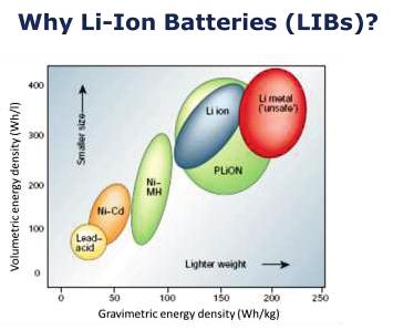
10 List of Figures Figure 1.1: Comparison of the different battery technologies in terms of volumetric and gravimetric energy density Figure 1.2: A schematic illustration of the working principles of a Li x C 6 /Li 1-x CoO 2 lithium-ion cell Figure 1.3: Li-Si system, (a) Equilibrium phase diagram, 34 (b) Voltage profile of the reaction of Li with Si at 415 C (red). 33 The voltage profile of the room temperature lithiation and delithiation of Si is also shown (black)...10 Figure 1.4: Voltage capacity curves for (a) microsized (1 10µm) and (b) nanosized ( nm) Si-anodes Figure 1.5: Voltage capacity curves for (a) micronsized (1 10µm) and (b) nanosized ( nm) Si-anodes. 39 (c) The differential capacity vs. potential curves for the 2 nd discharge/charge cycle of a pure Si thin-film anode Figure 1.6.: Schematic of morphological changes that occur in Si during electrochemical cycling Figure 1.7: (a) A statistical plot showing critical diameters ( nm) at which Si NWs start pulverizing. Green line shows the model prediction. (b) TEM images before (left) and after (right) the lithiation process to 10 mv vs. Li/Li +. Large nanowires disappear due to pulverization during the lithiation process, whereas the small nanowires remain in the same position Figure 1.8: The schematic of one representative as-synthesized and cycled silicon nanotube with SEI formation on the surfaces Figure 1.9: Specific capacity and Coulombic efficiency of silicon nanotubes cycled at rates of 0.05C (squares) and 0.2C (circles) Figure 1.10: The charge discharge profiles various carbons. (a) hierarchical porous carbon. 153 (b) Hard carbon Figure 1.11: Schematic of the electrochemical reaction process of hollow carbon nanospheres and solid carbon spheres Figure 1.12: (a) Cycling performance of RGO at 0.2 C and 1 C for 250 cycles (b) cycling performance of RGO at 1 C for 1000 cycles x
11 Figure 2.1: SEM image of the (a) SiNWs/SS, (b) SiNWs/TiN, (c) cross-sectional view of SiNWs/TiN, (d) histogram of the projected diameters of the individual Si NWs on TiN and on SS substrates Figure 2.2: SEM images of the (a) SiNWs/TiN, (b) 1Al/SiNWs, (c) 3Al/SiNWs, (d) 8Al/SiNWs, and (e) 13Al/SiNWs...43 Figure 2.3: TEM micrographs of bare and coated SiNWs. (a) (c) show TEM micrographs of the SiNW/TiN (a) bright field micrograph with corresponding indexed selected area diffraction (SAD) insert, (b) dark field micrograph, obtained using g ¼ 111Si with the wire oriented near the 112 symmetric zone axis, (c) HRTEM image of the SiNW structure. Fig. 3 (d) (f) show 1Al/SiNW. (d) Bright field micrograph with corresponding indexed SAD insert, (e) dark field micrograph of the Si obtained using g ¼ 111Si. (f) Dark field micrograph, obtained using a portion the 111Al ring pattern. (g) (i) show 3Al/SiNW. (g) Bright field micrograph with corresponding indexed composite SAD insert, (h) dark field micrograph of the Si obtained using g ¼ 111Si. (i) Dark field micrograph, obtained using a portion of the 111Al ring pattern, highlighting the nanocrystalline grain size of Al. Fig. 3(j) (l) show 13Al/SiNW. j) Bright field micrograph with corresponding indexed composite SAD insert, (k) dark field micrograph of the Si obtained using g ¼ 111Si. (l) Dark field micrograph, obtained using a portion of the 111Al ring pattern, highlighting the much coarser albeit still nanocrystalline grain size of Al Figure 2.4: Galvanostatic discharge/charge curves of the (a) SS spacer coated with TiN layer and (b) SS spacer without any coating layer...45 Figure 2.5: Galvanostatic discharge/charge curve of the (a) SiNWs/TiN, (b) SiNWs/SS, and (c) discharge capacity retention of the SiNWs/TiN and SiNWs/SS at 0.1 C rate...46 Figure 2.6: First lithiation response of SiNWs/SS highlighting the contribution of amorphous Si...47 Figure 2.7: XRD patterns of SiNWs/SS in as-made, lithiated and delithiated state...48 Figure 2.8: Cyclic voltammetry profiles of the (a) SiNWs/TiN, (b) 3Al/SiNWs, (c) 19Al/SiNWs, and (d) 50 nm of pure aluminum on TiN/SS substrate with the scan rate of 1 mvs xi
12 Figure 2.9: Galvanostatic discharge/charge curves of the (a) SiNWs/TiN, (b) 1Al/SiNWs, (c) 3Al/SiNWs, (d) 8Al/SiNWs, (e) 13Al/SiNWs, (f) 19Al/SiNWs, (g) first discharging, and (h) first charging cycle at 0.1 C rate. The contribution of Al to the electrochemical response is highlighted by arrows in Figure 2.9(h)...50 Figure 2.10: (a) Cycle life, (b) discharge capacity retention, and (c) coulombic efficiency of the uncoated and aluminum-coated SiNWs/TiN at 0.1 C rate...53 Figure 2.11: (a) Discharge capacity retention, and (b) first charging cycle of the 3Al/SiNWs at 0.2 and 0.1 C rate...54 Figure 2.12: SEM images of the (a) bare SiNWs after 100 cycles, (b) 1Al/SiNWs after 100 cycles, 3Al/SiNWs after (c) 30, (d) and (e) 100 cycles, and (f) 19Al/ SiNWs after 55 cycles...55 Figure 2.13: (a) and (b) show 1Al/SiNW. (a) bright field micrograph with corresponding SAD insert, (b) dark field micrograph taken from a portion of the 111Al ring. Fig. 2.13(c) (g) show TEM micrographs of the 3Al/SiNW. (c) and (f) bright field micrograph with corresponding SAD insert, (d) dark field micrograph obtained using a portion of amorphous Si ring, (e) HRTEMimage of the SiNW structure, (g) dark field micrograph obtained using a portion of amorphous 111Al ring. Fig. 11 (h) and (i) show a particle adjacent to the 19Al/SiNWs. (h) bright field micrograph with corresponding indexed selected area diffraction (SAD) insert, (i) dark field micrograph, obtained using g ¼ 200Al reflection...56 Figure 2.14: Cycling stability of bare SiNWs, 3Al/SiNWs and SiNWs coated with 4 wt.% Al 2 O 3 deposited by ALD...57 Figure 2.15: SEM micrographs of SiNWs/SS electrode (a) and (b) as-synthesized, (c) (e) after the first cycle. (c) and (d) near the SS substrate, (e) top-down view...58 Figure 2.16: Surface of the stainless steel substrate after polishing steps (a) and after lithiation/delithiation cycle and removal of the Si nanowires (b)...59 Figure 2.17: First and second cycles for SiNWs/SS (a) and 3Al/SiNWs/SS and 8Al/SiNWs/SS (b)...61 Figure 2.18: Impedance spectra of uncoated and Al coated SiNWs on TiN/SS substrate (a) assynthesized, (b) after 100 cycles...62 Figure 3.1: SEM images of (a) SiNWs, (b) (10)TiO 2-200/SiNWs, (c) (10)TiO 2-300/SiNWs, (d) (10)TiO 2-200(A)/SiNWs...74 xii
13 Figure 3.2: TEM micrographs of TiO 2 coated SiNWs. (a)-(d): (10)TiO 2-200/SiNWs. (a) Bright field micrograph, (b) corresponding indexed selected area diffraction (SAD), (c) dark field micrograph obtained using a portion of the diffuse halo of amorphous TiO 2 between the primary beam and the first set of Bragg reflections of Si, (d) dark field micrograph of the Si obtained using g =111 Si with the wire oriented near the 112 symmetric zone axis, (e) (h): (10)TiO 2-300/SiNWs. (e) Bright field micrograph, (f) corresponding indexed SAD, (g) Dark field micrograph obtained using a portion of the diffuse halo of amorphous TiO 2 between the primary beam and the first set of Bragg reflections of Si, (h) dark field micrograph of the Si obtained using g=111 Si. (i) (l): (10)TiO 2-200(A)/SiNWs. (j) Bright field micrograph, (j) corresponding indexed SAD showing the 011, 020 and 024 diffraction spots of anatase TiO 2, (k) dark field micrograph, obtained using g=011 TiO2, (l) dark field micrograph of the Si obtained using g =111 Si...75 Figure 3.3: Capacity retention vs. cycle number, expressed as a percentage relative to the first cycle capacity, for bare and TiO 2-200/SiNWs nanocomposites at different TiO 2 thicknesses cycled at 0.1 C rate, (b) specific capacity in mah/g and (c) corresponding coulombic efficiency...76 Figure 3.4: HRTEM images including fourier transforms (left and middle) and EELS maps (right) of (10)TiO 2-200/SiNWs, (a)-(c), (10)TiO 2-300/SiNWs (d)-(f), and (10)TiO 2-200(A)/SiNWs, (g)-(i). The areas delineated by the rectangles in (a), (d) and (g) are magnified by a factor 3 in (b), (e) and (h) which clearly show the lattice fringes for Si and, in the case of (10)TiO 2-200(A)/SiNWs, anatase TiO 2. The double-headed arrows in (a), (d) and (g) are the same length as the 10 nm scale bar. The HRTEM images and EELS maps show that the coating is at its nominal thickness...77 Figure 3.5: C1s, Si1s, O1s and Ti 2p XPS spectra of as-synthesized SiNWs, (10)TiO 2 /SiNWs at ALD deposition temperatures of 200 and 300 C and after annealing...78 Figure 3.6: Galvanostatic discharge/charge voltage profiles of (a) SiNWs, (b) (10)TiO 2-200/SiNWs, (c) magnification of the first 250 mah/g in the first discharging cycle at 0.1 C rate...80 Figure 3.7: Galvanostatic discharge/charge curves of 10 nm TiO 2 at ALD deposition temperature of (a) 200 C (b) 300 C, (c) after annealing treatment at 600 C for 1 hr at 0.1 C-rate...81 xiii
14 Figure 3.8: (a) Capacity retention vs. cycle number, expressed as a percentage of the first cycle capacity, for bare SiNWs and TiO 2 /SiNWs nanocomposites deposited at different temperatures and with annealing treatment at 0.1 C rate, (b) cycle life expressed as specific capacity, (c) corresponding Coulombic efficiency, and (d) comparison of the rate capability of bare SiNWs and the nanocomposites expressed as apercentage of the initial capacity at 0.1 C...82 Figure 3.9: (a) Bright-field TEM and SAD pattern of TiO 2-200/SiNWs, (b) HRTEM and FFT pattern of the same showing 200LiTiO 2 lattice spacing. (c) Ti XPS spectrum after 1 cycle of TiO 2-200/SiNWs, TiO 2-300/SiNWs and TiO 2-200(A)/SiNWs and (d) bright-field TEM and SAD pattern of TiO 2-200(A)/SiNWs...83 Figure 3.10: TEM micrographs of (a)-(c) (10)TiO 2-200/SiNWs, (c)-(f) (10)TiO 2-300/SiNWs, (g) and (h) (10)TiO 2-200(A)/SiNWs after 1 cycle (after delithiation to 2 V). (a), (d) and (g) bright field micrographs with corresponding selected area diffraction (SAD) insert. (b), (e) dark field micrographs using a portion of 200 LiTiO2 ring pattern, highlighting coarser grain size of LiTiO 2 in (d). (f) dark field micrograph of the TiO 2 obtained using g=101 TiO2. HRTEM images of (c) (10)TiO 2-200/SiNWs, and (f) (10)TiO 2-300/SiNWs, highlighting partial crystallization of LiTiO 2 phase embedded in the amorphous region...84 Figure 3.11: SEM images of (a) (10)TiO 2-200/SiNWs, (b) (10)TiO 2-300/SiNWs and (c) (10)TiO 2-200(A)/SiNWs after the first cycle at 0.1 C-rate...85 Figure 3.12: a) bright-field image of (10)TiO 2-200/SiNWs after 1 cycle between 0.01 and 3V vs. Li/Li + (b) corresponding SAD pattern confirming the cubic structure. (c)-(e) TEM micrographs of TiO 2-200(A)/SiNWs after 35 cycles (after lithiation to 0.01 V). (c) Bright field micrograph, (d) corresponding indexed selected area diffraction (SAD) pattern, (c) dark field micrograph using g=101 LixTiO2, (e) dark field micrograph obtained using g=200 LiTiO Figure 3.13: CV curves of planar TiO 2 films (a), deposited at 200 o C between 0.01 and 2V and (b) between 1 and 3 V vs. Li/Li +, (c) deposited at 300 o C and (d) annealed at 600 o C between 0.01 and 2V at a scan rate of 0.2 mv/s...87 Figure 3.14: Refractive index as a function of wavelength for 10 nm planar TiO 2 films on Si deposited at 200 and 300 o C...88 Figure 3.15: FIB cross-section SEM images of TiO 2-200/SiNWs, and TiO 2-200(A)/SiNWs together with elemental mappings of Silicon, Titanium, Carbon, Oxygen and Fluorine after 100 xiv
15 cycles at a rate of 0.1 C. The arrows indicate the locations of cracks that are forming between the nanowire agglomerate and the TiN layer on the substrate...88 Figure 3.16: SEM images of (a) SiNWs, (b) TiO 2-200/SiNWs, (c) TiO 2-300/SiNWs (d) TiO 2-200(A)/SiNWs after 100 cycles at 0.1 C...89 Figure 3.17: TEM micrographs of, (a) and (b),tio 2-200/SiNWs, (c) and (d), TiO 2-300/SiNWs and (e) and (f), TiO 2-200(A)/SiNWs after 100 cycles (after delithiation to 2 V). (a), (c) and (e) are bright field micrographs with corresponding SAD inserts. (b), and (d) dark field micrographs using a portion of the 200 LiTiO2 ring, (f) dark field micrograph using g=101 TiO Figure 3.18: SEM images of (a) (5)TiO 2-200/SiNWs, (b) (15)TiO 2-200/SiNWs at 0.1 C-rate after 100 cycles...90 Figure 3.19: TEM micrographs of (a) and (b) (5)TiO 2-200/SiNWs, (c) and (d) (15)TiO 2-200/SiNWs after 100 cycles. (a) and (c) are bright field micrographs with corresponding SAD insert. (b), and (d) dark field micrographs obtained using a portion of the 200 LiTiO2 ring pattern.91 Figure 3.20: HAADF images and EELS elemental maps of Si, Ti, O, Li and C of cycled (a) SiNWs, (b) TiO 2-200/SiNWs, (c) TiO 2-300/SiNWs and (d) TiO 2-200(A)/SiNWs after 100 cycles in the delithiated state...92 Figure 3.21: Capacity retention vs. cycle number for bare and (10)TiO 2-200/SiNWs nanocomposite at (a) 0.2 C-rate, (b) 0.5 C-rate, (c) Comparison of the % capacity retention of (10)TiO 2-200/SiNWs nanocomposite at different C-rates, and (d) comparison of the corresponding coulombic efficiency at different C-rates...93 Figure 3.22: SEM images of (10)TiO 2-200/SiNWs at (a) 0.2 C-rate, (b) 0.5 C-rate after 100 cycles...93 Figure 3.23: TEM micrographs of (10)TiO 2-200/SiNWs at (a) and (b) 0.2 C-rate, (c) and (d) 0.5 C-rate after 100 cycles. (a), and (c) bright field micrographs with corresponding SAD pattern insert. (b), and (d) dark field micrographs obtained using a portion of 200 LiTiO2 ring pattern...94 Figure 3.24: (a) TEM micrographs of (a) and (b) bare SiNWs, (c) and (d) (10)TiO 2-200/SiNWs and (e) and (f) (10)TiO 2-200(A)/SiNWs after 100 cycles at different rates according to Figure 3d (after delithiation to 2 V). (a), (c) and (e) bright field micrographs with corresponding SAD insert. (b), dark field micrograph using a portion of diffuse ring, (d) dark field micrographs using a portion of 200 LiTiO2 ring pattern, and (f) dark field micrographs using g=101 TiO xv
16 Figure 3.25: XPS spectra for bare SiNW electrode and electrodes coated with 10 nm TiO 2 after the first cycle...95 Figure 3.26: Li1s, F1s, O1s, C1s, Ti2p, P2p XPS spectra of 100 times-cycled SiNWs, TiO 2 - y/sinws at ALD deposition temperatures of 200 and 300 C and after annealing from the top surface of the electrodes in the delithiated state...96 Figure 3.27: Schematic microstructural illustration of the (a) and (b) bare SiNWs, (c) and (d) TiO 2 coated SiNWs for (a) and (c) as-grown, (b) and (d) cycled samples...98 Figure 4.1: SEM micrographs of (a) SiNTs, (b) SiNTs/TiO 2, (c) SiNTs/Al 2 O 3, (d) SiNTs/TiN electrodes. (e) FIB cross-section of SiNTs/TiO 2 showing the height of the nanotubes as approximately 3 µm Figure 4.2: TEM micrographs of the as synthesized materials. (a) and (b) uncoated SiNTs showing a bright field micrograph with the corresponding indexed SAD pattern, and a dark field micrograph of the polycrystalline Si obtained using a portion of 111 Si ring pattern. (c) Bright field micrograph and indexed SAD pattern of SiNTs/TiO 2, (d) SiNTs/Al 2 O 3, (e) SiNTs/TiN The TiO 2 and Al 2 O 3 coatings are amorphous whereas TiN is nanocrystalline Figure 4.3: TEM micrograph of the as synthesized materials, showing a bright field micrograph with the corresponding indexed SAD pattern, and a dark field micrograph of the polycrystalline Si obtained using a portion of 111 Si ring pattern. (a) and (b) TiO 2 /SiNTs/TiO 2 ; (c) and (d) TiO 2 /SiNTs Figure 4.4: HRTEM images including fast fourier transforms (FFTs) of (a)-(c) uncoated SiNTs; (d)-(f) and (d) SiNTs/TiO 2 ; and (g) (i) TiO 2 /SiNTs/TiO 2. High magnification images of areas marked by rectangles 1 and 2 highlight the lattice fringes for Si and the amorphous structure of the outer TiO 2 coating Figure 4.5: HAADF images and EELS maps of (a) uncoated SiNTs, (b) SiNTs/TiO 2, and (c) TiO 2 /SiNTs/TiO 2. Native oxide layers on Si are indicated with arrows. (d) line scan profile along the nanotube diameter (red dashed line) shows the hollow core-shell structure for TiO 2 /SiNTs/TiO 2 where 2 spikes in both the Ti and O signals spaced ~20 nm apart are visible on either end of the scanned area Figure 4.6: XPS spectra of the TiO 2 -coated SiNTs electrodes in as-synthesized state xvi
17 Figure 4.7: Constant current voltage profiles and differential capacity curves, tested at 0.2 C, at 1, 2, 20, 50 and 100 cycles. (a) and (b) SiNTs; (c) and (d) TiO 2 /SiNTs/TiO 2. (e) Magnification of the first 800 mah/g in the first discharging cycle at 0.2 C rate Figure 4.8: Constant current voltage profiles and differential capacity curves, tested at 0.2 C, at 1, 2, 20, 50 and 100 cycles. (a) and (b) SiNTs/TiO 2, (c) and (d) TiO 2 /SiNTs. (e) Magnification of the first 50 mah/g for TiO 2 /SiNTs in the first discharging cycle at 0.2 C rate. (f) Magnification of the dc/dv for the TiO 2 /SiNTs in the first discharging cycle at 0.2 C. They highlight the plateau and the related peak in the dc/dv profile for TiO 2 /SiNTs sample corresponding to the lithiation of anatase TiO Figure 4.9: a) and (d) Al 2 O 3 /SiNTs, b) and (e) SiNTs/Al 2 O 3, (c) and (f) /Al 2 O 3 /SiNTs/Al 2 O 3. (g) Magnification of the first 800 mah/g in the first discharging cycle at 0.2 C rate Figure 4.10: (a) and (d) TiN/SiNTs, (b) and (e) SiNTs/TiN, (c) and (f) /TiN/SiNTs/TiN. (g) Magnification of the first 800 mah/g in the first discharging cycle at 0.2 C rate Figure 4.11: (a) and (b) Capacity retention vs. cycle number for SiNT s coated with 3 nm of Al 2 O 3, TiN, and TiO 2 on their outer surface, tested at 0.2 C rate; (c) corresponding Coulombic efficiency; and (d) rate dependence of capacity retention as a percentage of capacity at 0.2 C..120 Figure 4.12: XPS spectra of the electrodes in the as-synthesized state and after 100 cycles. (a) - (e) SiNTs, SiNTs/Al 2 O 3, SiNTs/TiN, SiNTs/TiO 2. (f) Al2p spectra for SiNTs/Al 2 O 3, (g) Ti2p spectra for SiNTs/TiO 2 and SiNTs/TiN Figure 4.13: (a) and (b) Capacity retention vs. cycle number of TiO 2 coated SiNTs, highlighting the role of coating location, i.e. inner surface, outer or both. (c) Corresponding Coulombic efficiency Figure 4.14: (a) and (b) Capacity retention vs. cycle number of Al 2 O 3 coated SiNTs, highlighting the role of coating location, i.e. inner surface, outer or both. (c) Corresponding coulombic efficiency Figure 4.15: (a) and (b) Capacity retention vs. cycle number of TiN coated SiNTs, highlighting the role of coating location, i.e. inner surface, outer or both. (c) Corresponding coulombic efficiency Figure 4.16: Impedance spectra for as-synthesized, (a), after 100 cycles in delithiated state, (b) for bare SiNTs and inner, outer and double-sided TiO 2 -coated SiNTs xvii
18 Figure TEM micrographs of the post 100 cycles delithiated microstructures. (a) and (b) bare SiNTs. The dak field micrograph was taken using a portion of the diffuse amorphous ring. (c) and (d) TiO 2 /SiNTs, (e) and (f) SiNTs/TiO 2, (g) and (h)tio 2 /SiNTs/TiO 2. In (d), (f) and (h) the dark field micrographs were taken using a portion of the 200 LiTiO2 ring Figure 4.18: FIB cross-sections (top row) and plane-view SEM images (bottom row) after 100 cycles of bare SiNTs (a and e), TiO 2 /SiNTs (b and f), SiNTs/TiO 2 (c and g) and TiO 2 /SiNTs/TiO 2 (d and h) Despite the original structure of the nanotubes still being recognizable for all electrodes, SiNTs and TiO 2 /SiNTs clearly show more structural damage compared to and TiO 2 /SiNTs/TiO 2, in agreement with cycle life and CE data Figure 4.19: (a) and (b) SiNTs/Al 2 O 3. For Al 2 O 3, the dark-field micrograph was taken using a portion of the diffuse amorphous ring, (c) and (d), SiNTs/TiN, with the TiN nanocrystallites being imaged in dark field using a portion of 111 TiN ring pattern Figure 4.20: Microstructure after 100 cycles. HAADF images and EELS elemental maps of Si, Ti, O, Li and C of (a) SiNTs; (b) TiO 2 /SiNTs. (c) SiNTs/TiO 2 ; (d) TiO 2 /SiNTs/TiO 2 ; In (a) the Si map was obtained from the region marked by the dashed rectangle, while the other elements were obtained from the region marked by the solid rectangle. In (b) only Li, Si and C together, Ti and O together were obtained from the regions marked by the dashed rectangle, the dotted rectangle and solid rectangle, respectively Figure 5.1: (a) Environmental SEM image of a cross-sectioned dried banana peel. (b)-(c) Low magnification SEM micrographs of banana peel pseudo graphite (BPPG) carbonized at 800 C and activated (b) and at 1400 C and activated (c). (d) SEM images of baseline commercial graphite (CG), and (e) baseline NORIT Supra activated carbon (AC), highlighting the overall morphology of the materials employed as electrochemical testing baselines Figure 5.2: Figure 5.2: Structure of banana peel pseudo graphite (BPPG) in its activated state. (a) A SEM micrograph highlighting the general morphology of a BPPG particle (BPPG-1100-A), with the inset showing its volume difference in comparison with baseline commercial graphite (CG) and activated carbon (AC) of the same weight. (b) Pore size distribution (calculated from the adsorption isotherms using DFT method) with the inset showing nitrogen adsorptiondesorption isotherms. (c) and (d) XRD and Raman spectra. (e)-(g) HRTEM micrographs of BPPG-800-A, BPPG-1100-A and BPPG-1400-A, respectively. The corresponding data for BPPG is shown in Figure 5.3(a)-5.3(b) xviii
19 Figure 5.3: (a) Nitrogen adsorption-desorption isotherms of BPPG. (b) Pore size distribution calculated from the adsorption isotherms, using DFT method. (c) XRD patterns of the unactivated specimens (BPPG). (d) Raman spectra of BPPG Figure 5.4: Fitted Raman spectra of BPPG-A specimens. (a) BPPG-800-A, (b) BPPGA-1100-A, and (c) BPPG-1400-A Figure 5.5: XPS survey spectra of the (a) and (b) as-synthesized, (c) and (d) mechanically ground BPPGA and BPPG specimens Figure 5.6: Electrochemical performance of BPPG, tested in a half cell against Na. (a) Cyclic voltammogram (CV) of BPPG-1100-A, tested at 0.1 mv s -1. (b) Galvanostatic discharge/charge curves of BPPG-1100-A at a current density of 50 mag -1. (c) Potential profiles of BPPG and BPPG-A electrodes, (d) Summary of capacity versus potential distribution of BPPG and BPPG- A, 10 th cycle at 50 mag -1. (e) Dependence of the mean graphene interlayer spacing of BPPG A on discharge/charge voltage, demonstrating reversible Na intercalation-induced dilation of the mean intergraphene spacing. The electrodes were galvanostatically discharged/charged to 0.2, 0.1, 0.05, and V, with dilation values derived from XRD spectra shown in Figures (f) The Raman integral intensity ratio (I G /I D ) of BPPG-1400-A as a function of discharge/charge voltage demonstrating intercalation-induced ordering of the carbon, values derived from Raman spectra in Figure Figure 5.7.: CV and galvanostatic discharge/charge profiles of (a)-(c) BPPG-800-A, and (d)-(f) BPPG-1400-A electrodes. CVs were done between and 2.8 V vs. Na/Na + at a scanning rate of 0.1 mvs -1. Galvanostatic discharge/charge profiles are obtained at current density of 50mAg Figure 5.8: CV and galvanostatic discharge/charge profiles of (a)-(c) BPPG-800, (d)-(f) BPPG- 1100, and (g)-(i) BPPG-1400 electrodes versus Na Figure 5.9: (a) Volumetric capacity of BPPG-1100-A tested against Na, at a current density of 50mAg -1. Capacity calculation is based on the true density of BPPG, which is ~ 2 g/cm 3. (b) Cross section SEM image of a drop-cast BPPG-1100-A electrode, as electrochemically tested in this study. (c) Cross section SEM image of a pressed high mass loading BPPG-1100-A electrode Figure 5.10: (a) XRD spectra for BPPG-1400-A at different discharge and charge voltages versus Na. (b) Raman spectra for BPPG-1400-A at different discharge and charge voltages versus Na. xix
20 (c)-(f) High resolution Na 1s, and C 1s XPS spectra for sodiated and desodiated BPPG-1400-A, analyzed after 10 cycles. 5.10(c) and 5.10(d) show spectra for samples where the electrode's top SEI covered surface was removed by the scotch tape method. 5.10(e) and 5.10(f) show spectra for samples without the top layer removed, i.e. intact electrode covered by SEI. (a) XRD spectra for BPPG-1400-A at different discharge and charge voltages versus Na. (b) Raman spectra for BPPG-1400-A at different discharge and charge voltages versus Na. Na 1s, and C 1s high resolution XPS spectra for sodiated and desodiated BPPG-1400-A after 10 cycles Figure 5.11: Low magnification SEM micrograph of BPPG-1400-A desodiated to 2.8 V, after 10 cycles. 5.11(a) shows the electrode morphology after the electrode's top layer was removed by the scotch tape method, 5.11(b) shows the morphology of an intact electrode that is covered by SEI Figure 5.12: (a) Cycling performance of the BPPG and BPPG-A electrodes tested in a half cell against Na, with the corresponding coulombic efficiency (CE) being displayed on the right axis. (b) Extended cycling performance and CE of the BPPG-1100-A electrode. (c) Rate performance of BPPG-A electrodes. (d) Rate performance of BPPG electrodes. (e) (f) Cycling capacity retention and rate capability comparison of BPPG-1100-A with the state-of-the-art in literature, tested versus Na. Red diamonds are our results Figure 5.13: Equivalent electronic circuits used to simulate the electrochemical impedance spectra (EIS) results. For the spectra of all the as- prepared specimens, equivalent circuit (a) was used. For the cycled specimens with an SEI layer formed, equivalent circuit (b) was used Figure 5.14: Experimental EIS of as-prepared BPPG-A, and BPPG electrodes versus (a) Na, (b) Li. Experimental EIS of BPPG-A, and BPPG electrodes after 300 cycles versus (c) Na, (d) Li 160 Figure 5.15: (a)-(c) EIS of BPPG-800-A, BPPG-1100-A, and BPPG-1400-A versus Na, for cycles (d) EIS of BPPG-1100-A versus Li for cycles (e) The total charge transfer resistance within all the interfaces (R ct +R f ),as a function of cycle number. (f) R el as a function of the cycle number Figure 5.16: Electrochemical performance of BPPG, tested in a half cell against Li. (a) Cycling performance of the BPPG-A electrodes, with coulombic efficiency of electrodes being displayed. (b) Rate performance of BPPG-1100-A electrode. (c) XRD spectra for BPPG-1400-A at different discharge and charge voltages (vs. Li/Li + ). (d) Dependence of the mean graphene interlayer spacing of pseudo graphite (black line) and graphite (blue line) phases in BPPG xx
21 A on the discharge/charge voltage. The electrodes were galvanostiatically discharged/charged to 0.2, 0.1, 0.05, and V, 10 th cycle at 50 mag -1. (e) (f) Cycling capacity retention and rate capability comparison of BPPG-1100-A with the state-of-the-art in literature, tested versus Li. (The current density in reference 99 and 102 is based on Acm -2 ). Red diamonds are our results Figure 5.17: Electrochemical performance of BPPG-A, tested in a half cell against Li metal from and 2.8 V. (a) CV of BPPG-1100-A, tested at 0.1 mv/s. Galvanostatic discharge/charge curves of (b) and (c) BPPG-800-A, (d) and (e) BPPG-1100-A, (f) and (g) BPPG-1400-A at a current density of 50 ma/g Figure 5.18: Galvanostatic discharge/charge curves of (a) and (b) BPPG-800, (c) and (d) BPPG- 1100, (e) and (f) BPPG-1400, versus Li Figure 5.19: Electrochemical performance of BPPG, tested in a half cell against Li, 10 th cycle at 50 mag -1. (a) Potential profiles of BPPG and BPPG-A electrodes, (b) Summary of capacity above and below 0.1 V in BPPG and BPPG-A Figure 5.20: (a) Raman spectra for BPPG-1400-A at different discharge and charge voltages versus Li. The electrodes were galvanostiatically discharged/charged to 0.2, 0.1, 0.05, and V. (b) The Raman integral intensity ratio (I G /I D ) as a function of discharge/charge voltage demonstrating intercalation-induced ordering of the carbon, values derived from Raman spectra in Figure 5.20(a) Figure 5.21: Li 1s, and C 1s high resolution XPS spectra for lithiated and delithiated BPPG A after 10 cycles Figure 5.22: Low magnification SEM micrograph of BPPG-1400-A delithiated to 2.8 V, after 10 cycles. 5.22(a) shows the electrode morphology after the electrode's top layer was removed by the scotch tape method, 5.22(b) shows the morphology of an intact electrode covered by SEI.170 xxi
22 List of Tables Table 1.1: The comparison between Na and Li elements...22 Table 2.1: The capacity and coulombic efficiency of the SiNWs/TiN and Al/SiNWs electrodes in the first cycle...51 Table 3.1: Galvanostatic electrochemical results obtained for the bare and TiO 2 coated SiNWs nanocomposites at 0.1 C- rate...79 Table 3.2: Surface composition, in atomic percentages, as derived from the XPS spectra in Fig Figure 3.24 and Figure 3.25 for 1 and 100 times cycled electrodes...97 Table 4.1: Galvanostatic cycling results for the uncoated and coated SiNW electrodes, tested at 0.2C Table 4.2: Comparison of capacity at different rates and coulombic efficiency of different hollow Si-based structures Table 5.1: Structure and textural properties of BPPG and BPPG-A Table 5.2: Elemental composition information for BPPG and BPPG-A Table 5.3: XPS results on BPPG and BPPG-A that were mechanically ground after synthesis so as to expose bulk material to surface analysis Table 5.4: Coulombic efficiency and cycling capacity of BPPG and BPPG-A, versus Na. Samples were activated at 0.05 A/g for 10 cycles and were subsequently tested at 0.1 A/g Table 5.5: Resistance values simulated from modeling the experimental impedance (Figure 5.13) using the equivalent circuits shown in Figure Table 5.6: Plateau capacity (below 0.1 V) comparison of BPPG-1100-A versus state-of-the-art NIB carbons Table 5.7: Coulombic efficiency and cycling capacity of BPPG and BPPG-A, versus Li. Samples were activated at 0.05 A g -1 for 10 cycles and were subsequently tested at 0.1 A/g Table 5.8: Performance comparison of BPPG-1100-A versus state of the art LIB carbons reported in literature xxii
23 1 Introduction Currently, ~80% of the global energy consumption relies mostly on the usage of nonrenewable fossil fuel with serious energy, environmental, health and climate concerns, and therefore, it is non-sustainable. Thus, the arrival of a new era of green renewable energy including solar and wind powers is expected to support a more sustainable economic growth. 1-8 However, it is difficult to use these kinds of energy for transportation such as vehicles due to their uneven energy production. One promising alternatives is driving electric vehicles which can significantly relieve the environmental pollution. 6,8,10,11 However, the utilization of electric cars requires highly efficient energy storage devices. In this regard, lithium- ion batteries (LIBs) can play an important role. 5-8,12 LIBs have been widely used in portable electronic devices such as computers, tablets, mobile phones, and medical microelectronic devices due to their high energy density and long cycle life. However, there are still many existing problems to be overcome for their broad and practical applications in stationary energy storage and electric vehicles. 5, For example, the amount of energy density they provide is still not enough to be competitive with liquid fuels and the driving range of most full electric cars is still well below the one of gasoline-powered vehicles. 15 Therefore, it is demanding to further increase their energy and power densities, improving their safety, and lowering the cost. 5,14, Batteries Batteries use a driving force, which is the difference in oxidation or reduction potential, to accept or give away electrons, between two species or electrodes. The two species consist of a metallic current collector allowing the electron flow from the external circuit to the electrodes in which they provide useful work, for example power a portable device such as a cellular phone or an electric vehicle. The two electrodes are separated, physically and electronically, by an ionically conducting and electronically insulating electrolyte. In order to mechanically separate electrodes and to prevent short-circuits, a separator is also used, which is made of glass, cellulose, or polymer fibers. The electrode with stronger reducing potential to give up electrons and become oxidized is the negative electrode (anode). Lithium is the strongest reductant on the periodic table with a strandard reduction potential of V. The electrode which accepts the electrons from the negative electrode and become reduced is the positive electrode (cathode). 1
24 During discharge, an electrochemical oxidation reaction proceeds at the negative electrode and at the same time an electrochemical reduction reaction proceeds at the positive electrodes by accepting the electrons passing through the external circuit. The electron transfer process will occur until the potential difference between the two electrodes becomes too low. At this point, the cell is fully discharged. 17,18 The change from electronic current to ionic current occurs at the electrode/electrolyte interface. Faraday s Law, which is the relationship between the equivalent quantities of chemical reactants and electrical charge, governs this change. In secondary batteries, the reverse process can be performed using external energy, known as the charge. During the charge process, the electrons flow from positive to the negative electrode and the potential difference between the two electrodes can be reinstated. In both cases, the transfer of electrons through the circuit from one electrode to another is balanced by the transfer of positively charged ions (cations) in the electrolyte. There are two main types of batteries: primary batteries (non-rechargeable batteries) and secondary batteries (rechargeable batteries). In a secondary battery, the redox reactions and structural changes can be reversed by running a current into the cell with a battery charger to recharge it, regenerating the chemical reactants and allowed to discharge again. Primary batteries usually have good shelf time, energy and power density, and low cost and are typically used as hearing aides, watches, smoke alarms, and some portable electronics such as cameras. However, the secondary batteries with lower total cost of use and environmental impact have become the most commonly used batteries todays and are now a common place in all cell phones, laptops, digital cameras, and mp3 players. Among the various existing technologies (Figure 1.1), Li-based batteries currently outperform other types of secondary batteries due to their high gravimetric and volumetric energy densities and design flexibility. 18 This allows them to be lighter and take up less space. Moreover, with superior power densities, they can recharge more quickly than other types of batteries. These advantages result from using the light-weight lithium containing compounds and a non-aqueous electrolyte that can allow for a larger voltage range between the two electrodes. Because the energy density is related to this voltage range, a large voltage will yield a higher energy density. They account for 63% of worldwide sales values in portable batteries. 19 This explains why they receive most attention at both fundamental and applied levels. 2
25 3

26 per every 6 C atoms. This leads to a theoretical capacity of 372 mah/g. Moreover, as the Li insertion occurs at about 0.1 V vs. Li/Li +, there is the added benefit of a safer operating potential, while still maintaining a high cell voltage and energy density. A schematic of a lithium battery with a graphite negative electrode and a lithium metal oxide (Li 1-x CoO 2 ) positive electrode, which are connected through an external circuit, has been illustrated in Figure 1.2. During discharging, lithium ions diffuse from a lithiated graphite (Li x C 6 ) structure (negative electrode) into a delithiated Li 1-x CoO 2 structure (the cathode) with concomitant oxidation and reduction of the two electrodes, respectively. Accordingly, the negative electrode contracts as lithium ions are deintercalated from graphite and inserted in the positive electrode through the electrolyte, while electrons flow towards the positive electrode through an external circuit. During charging process, electrons are driven from the positive electrode to the negative electrode through the external circuit by an external power source. For maintaining the neutrality, lithium ions are displaced from the positive electrode towards the negative electrode through the electrolyte. The expansion of the negative electrode takes place by lithium ions insertion. Figure 1.2: A schematic illustration of the working principles of a Li x C 6 /Li 1-x CoO 2 lithium-ion cell. (adapted from 24). 4
27 1.1.2 Important parameters for evaluating battery electrode materials Voltage The difference between the standard Gibbs free energy of formation (ΔG f) of the products and the reactants is the driving force for a reaction which follows as: ΔG rxn=σ (products)-σ (reactants) (1) This chemical driving force is equivalent to an electrostatic driving force (-nef) where, E is the voltage between the electrodes, n is the stoichiometric number of electrons involved in the reaction and F is the Faraday s constant. Accordingly, a theoretical voltage for that reaction equals to: (2) The voltage of a battery in Li-ion batteries is equivalent to the difference in chemical potential of lithium in each electrode. The voltage between the two electrodes when the cell is at open circuit and not discharged yet equals to: ( ) ( ) (3) Where, ( ) and ( ) is the chemical potential of Li in the negative and positive electrode, respectively. When the cell is fully charged, > and the voltage is positive. Li + ions transfer from the higher chemical potential in the negative electrode to the lower chemical potential in the negative electrode when current flows upon closing the circuit. Upon discharging, chemical potential change for lithium in each electrode when a reaction occurs can be expressed by the Nernst equation: Where, ( ) Li ( ) Li is the chemical potential of species i in its standard state, a i is the activity of species, T is the temperature and R is the ideal gas constant (8.314 J/mol.K). Since the activity of a species is its effective concentration, the Nernst equation indicates that the chemical potential and subsequently, the voltage changes as a function of the amount of Li in each electrode. Typically the potential change is monitored over time. Accordingly, the capacity can be determined from the potential-time relation. (4) 5
28 There are two groups and three different types of lithium reaction with a metal or alloy, which could be divided as: A: 1) solid-solution reaction and 2) addition reaction; B: 3) displacement or conversion reaction. 25 When lithium ions are added in the reactant phase without displacing components from the reactant, it is referred to group A reaction which follows as: (5) Where, M can be element or a compound. Group A can be divided into solid-solution and addition reactions depending on whether or not a phase transformation occurs in the reactant M when lithium ions are inserted into the structure. When a phase change occurs from M to LiM x, it is referred to an addition reaction. For example, lithium insertion/extraction in crystalline Si, Al and Sn are addition reactions since lithium has a very limited solubility in these elements. In displacement reaction, lithium reacts with one component of the reactant, while the other component, which could be active or inactive towards lithium, is displaced or extruded from the reactant. The corresponding reaction follows as: (6) Some displacement reactions are irreversible and the displaced element does not participate in the subsequent reactions and acts as a buffering matrix. Accordingly, the reaction becomes an addition reaction for the other element. When the displaced element is active, it reacts with lithium at potential lower than that the other element and the reaction becomes an addition reaction for the active element as well as a displacement reaction according to the reaction (6). The Gibbs phase rule is useful for understanding why a voltage curve can be so important for understanding the electrochemical reactions of a material. The Gibbs phase rule for nonreactive processes states that: F=C-P+2 (7) Where, F is the number of degree of freedom, C is the number of independent components and P is the number of phases in the system. The quantity of F indicates the number of intensive thermodynamic parameters to define the system and its related properties e.g. the chemical potential and thus, voltage. For a solid-solution reaction, the degree of freedom equals to three. Concerning that the electrochemical reactions are measured at specific temperature and pressure, only one parameter is required for defining the system. Since lithium is added to the 6
29 system, its concentration in LiM x changes during the reaction. So the concentration of lithium in LiM x could be the final parameter. Based on this, the potential, where only one phase exists, varies with the lithium concentration at constant temperature and pressure. In this case, the voltage profile has a sloping shape. For an addition reaction in a binary system, the chemical potential is two degree of freedom. At constant temperature and pressure, there is no parameter to be defined and thus, the potential is independent of the lithium concentration. The voltage profile is a constant plateau. Finally, the equilibrium potential of a displacement reaction in a ternary system Li-M-N, where three phases exist, is independent of the lithium concentration Capacity The amount of charge that material can store is defined as the capacity of an electrode. Typically, capacities are reported in terms of gravimetric specific capacities, or the amount of stored charge normalized by the mass of the material. For the applications where the size of the battery is more important than its weight, the volumetric specific capacities are used. Capacities are often reported in units of ampere-hours per gram for batteries. Because an ampere is a Coulomb/sec, an ampere-hour is just another way of representing the charge. The capacity of an electrode for LIBs can be calculated if the stoichiometry of the lithiated material, Li x A is known as one electron is transferred for every Li ion. The specific (gravimetric) capacity, C G, and volumetric capacity, C v, can be calculated from the following equations: (8) (9) Where F is Faraday's constant ( x 10 4 C), and M w and ρ are the molecular weight and density, respectively, of the host material A, and x is the amount of Li in Li x A, The Coulombic efficiency (CE) is ratio (expressed as a percentage) between the energy removed from a battery during discharge compared with the energy used during charging to restore the original capacity: 7
30 ( ) (10) The Coulombic efficiency shows the reversibility of the lithiation process. The CE lower than 100% means some charge is lost and used for processes other than the reversible lithiation/delithiation reactions such as the irreversible trapping of Li in the host material and the formation of solid electrolyte interphase (SEI) due to the decomposition of the electrolyte at low potentials. However, this irreversible capacity loss is observed only in the first few cycles after which, the lithiation process becomes more reversible and the SEI layer has passivated the surface of the material, leading to very little irreversible capacity loss and high CE in subsequent cycles. It is worth noting that the electrolyte is reduced prior to lithiation for the formation of the passivating SEI layer on negative electrode surfaces to inhibit electron transfer between the electrolyte and electrode. 17 The large volume change in silicon negative electrodes leads to the SEI breakage and continual growth resulting in large irreversible capacity loss Energy density The specific energy, E, of an electrode material can be calculated from the specific capacity and the average potential at which the reaction with lithium occurs, V. (11) The specific energy (gravimetric energy density) is typically reported in units of Wh/kg while the volumetric energy density is reported in Wh/L. According to the equation above, there are two options to increase the energy of the battery, 1. Increase the specific capacity or 2. Increase the voltage. When considering only the active materials of the positive and negative electrodes, the energy densities of ~560 Wh/kg are obtained for LiCoO 2, LiMn 2 O 4, or LiFePO 4 against graphite. However, the gravimetric energy density of the entire battery is lower by about 50-70% than the theoretical one as the weight of the electrolyte, separator, current collectors, and other inactive components must be considered. 26 It should be noted that if the potential changes dramatically during the lithiation/delithiation process, then the energy density will also change. Some electrode materials that display high specific capacities have poor voltage characteristics, resulting in minimal improvements in the energy density. Thus, it is always important to consider both the voltage and specific capacity when looking at possible new electrode materials. 8
31 Power The power a battery can supply is related to the magnitude of the current drained during the discharge. Typically, the larger the current, the higher the IR losses and polarization effects. Moreover, the problem could be related to the phase transformations and solid-state diffusion in the active materials. All of these factors may change the shape of the discharge curve as well as lower the capacity and voltage the battery can deliver. Therefore, batteries are typically measured at different currents. "C" rates are used to identify the currents used in galvanostatic (constant current) measurements. 1C is defined as the amount of current needed to fully discharge the battery in one hour. This can be calculated from the theoretical capacity, C G, and the mass of available material, m: (12) Silicon as a LIB negative electrode Silicon is one of the most promising negative electrode materials owing to its large charge storage capacity of 3590 mah/g, corresponding to Li 15 Si 4, which is ten times higher than graphite (372 mah/g corresponding to the formation of LiC 6 ) Silicon is also the second most abundant element on earth. Because of these attributes, a great deal of attention has been given to using Si as a Li ion cell negative electrode material. Wen and Huggins 33 in an early study have shown that at 415 C, the electrochemical reaction of lithium with silicon follows the equilibrium Li Si phase diagram. Based on the phase diagram in Figure 1.3(a), the reaction products are Li 12 Si 7, Li 7 Si 3, Li 13 Si 4 and Li 22 Si 5 with the onset potentials of 332, 288, 158, and 44 mv, respectively. The final phase gives a specific discharge capacity of about 4200 mah/g based on the weight of Si However, the Li Si reaction at room temperature does not appear to follow this scheme. 9
32 (a) (b) Figure 1.3: Li-Si system, (a) Equilibrium phase diagram, (adapted from 34) (b) Voltage profile of the reaction of Li with Si at 415 C (red). (adapted from 33). The voltage profile of the room temperature lithiation and delithiation of Si is also shown (black). In 1999, Huggins et. al. investigated the system at room temperature using the stoichiometric equilibrium phases. 33 They found out the delithiation of these compounds occurred in two-phase regions, but the expected voltage profile for the formation of increasingly Li-poor phases was not observed (see Figure 1.3(b)). Instead, the two-phase region was maintained until most of the Li was removed. During delithiation, a voltage hysteresis of about 0.4 V was observed. Interestingly, Li could be re-inserted into the discharged Si in two sloping voltage regions. Moreover, the cycling voltage curves are influenced by both the Si particle size and the depth of lithiation. 35 The typical voltage curves observed for Si negative electrodes with the particle sizes of few microns is shown in Figure The first lithiation curve exhibits a single flat plateau at around 0.1 V, indicating a twophase addition reaction rather than the multi-phase reactions predicted by the equilibrium Li Si phase diagram. Moreover, the subsequent lithiation shows sloping plateau voltage curves. Meanwhile, there is a strong dependence between the cut-off potential of lithiation and delithiation voltage curves. If the negative electrode is fully lithiated to 0 V, the delithiation curves exhibit a single flat plateau at around 0.4 V in all the cycles, followed by an upwardly sloping region (Figure 1.4(a)). However, if the negative electrode is lithiated to above 50 mv, the delithiation curves show a sloping plateau (Figure 1.4(b)). 10
33 (a) (b) Figure 1.4: Voltage capacity curves for Ni 30 Si 70 alloy (a) lithiated to 0 V and (b) lithiated to 50 mv for the first two cycles and then to 70 mv for later cycles. (adapted from 38). Detailed XRD studies indicated that at voltages above 50 mv, the crystalline Si particles are transformed to amorphous Li x Si in the first lithiation process. A distinct plateau is observed as it is a two-phase addition reaction. Below 50 mv, the amorphous phase is suddenly crystallized to Li 15 Si 4 with the subsequent flat plateau at around 0.4 V during delithiation. Then, it is followed by a solid-solution reaction from amorphous Li z Si to amorphous Si. 42 When the negative electrode is lithiated to above 50 mv, the formation of crystalline Li 15 Si 4 phase is suppressed and the final product will be amorphous Li x Si. Then, the subsequent delithiation process is a solid-solution reaction from amorphous Li x Si to amorphous Si without phase change, leading to a sloping voltage curve. Another parameter which changes the voltage profiles of Si negative electrodes is the Si particle size. For Si particles of nm, it shows a sloping delithiation voltage profile with no distinct plateau, even if the negative electrodes are fully lithiated to 0 V. 39,43-46 Figure 1.5(a) and (b) shows the voltage profile of the micron-sized Si sample with a flat delithiation plateau at around 0.4 V but a sloping profile for the nanosized sample ( nm) even after fully 11
34 lithiated to 0 V. 39 When the Si particle sizes are further reduced to less than 20 nm, even the flat plateau in the first lithiation process turns to a sloping shape. 47,48 For those sloping voltage curves, two broad peaks are often observed on the corresponding differential-capacity (dq/dv) plots in both the lithiation and delithiation branches (see Figure 1.5(b)). The peak potentials of most Si-alloys appear at ~0.06 V and ~0.25 V for lithiation, and ~0.3 V and 0.5 V for delithiation. It has been reported that the voltage curves and phase transformation in amorphous Si thin-film negative electrodes are affected by the film thickness, surface roughness and alloy additions. 41,47,48 The critical thickness for the crystalline Li 15 Si 4 phase in amorphous Si films and subsequently, the appearance flat plateau in the delithiation process is ~2 µm. 41 However, it has been observed that in a multilayer amorphous Fe/Si negative electrode the crystallization occurs for the Si thickness larger than 200 nm. But the formation of crystalline Li 15 Si 4 phase is suppressed when the film is deposited on a rough surface. The relatively low critical thickness for crystallization in the Fe/Si films as compared to pure Si films may be due to the promoting effect of Fe/Si interfaces on the crystallite nucleation. 47 (a) (b) Figure 1.5: Voltage capacity curves for (a) micronsized (1 10µm) and (b) nanosized ( nm) Si-anodes. 39 (c) The differential capacity vs. potential curves for the 2 nd discharge/charge cycle of a pure Si thin-film anode. (adapted from 49). 12
35 An important feature observed in silicon-based materials is the large inherent change in specific volume (>300%) associated with lithium insertion and extraction. The stresses induced by these volume changes lead to high internal stress, pulverization and electrical disconnection from the current collector. This induces a significant capacity loss and short cycle life and subsequently, limits the commercial use of silicon in lithium cells Many efforts have been made in recent years to improve the cycling stability, such as decreasing the structures to nanosize or using the thin films or nanoparticles. There have been a large number of studies on the electrochemical reaction of Li with Si and subsequent cycling behavior. Several electrode morphologies and architectures have been explored, including nanopillars, 56,57 particles, porous structures, various composite negative electrodes, thin films, nanowires (NWs), and nanotubes (NTs) As we will discuss with more details in the next part, nanosized silicon-based negative electrodes can improve cycling by accommodation the large volume change without structural degradation during lithiation/delithiation process. They could also improve cycling by exploiting short lithium diffusion distances within the electrode and large surface area resulting in high rate capability. 85, Advantages of nanostructured or nanoscale electrodes Nanostructured or nanoscale electrodes can provide the necessary volume of free space to accommodate alloying induced expansion/contraction. Thus, they can minimize material stress and electrode pulverization to achieve greater reversibility and cycling stability Nanoscale dimensions allow quick relaxation of stress, making nanoparticles more resistant to fracture than bulk particles. Comparison of the calculated misfit stress energy in partially delithiated particles (consisting of a lithiated core and delithiated shell) suggests fracture should not occur during cycling for particles having diameters of 10 nm or less. 90 As mentioned above, different Si nanostructures have been contemplated to mitigate volumetric changes of Si-based negative electrode materials. Several methods have been used to reduce the capacity fading of Si-based negative electrode materials. One strategy is the reduction of Si particle size to nanometres, which is helpful to decrease the lithium ion diffusion path length, and improve the capacity retention of Si-based negative electrodes. However, it has failed to completely exclude capacity fading. When metal nanoparticles are used as a negative electrode material, the nanoparticles undergo aggregation and pulverization during cycling. 91,92 More attractive strategy is to 13
36 fabricate NWs and NTs in order to better accommodate the large volume change during lithium insertion/extraction compared to micro- and nanoparticles. The use of nanoscale morphologies may also improve the rate capability and specific capacity. As expected, the capacity of silicon electrodes decreases at high charge/discharge rates as a result of the low lithium ionic conductivity in silicon and sluggish mass transfer at the electrode interface. By reducing the electrode dimension and increasing the surface-to-volume ratio shorter lithium diffusion distances can be provided. Thus, the electrode polarization may be reduced, allowing high capacities to be realized Nanostructure morphologies-nanowires The nanowire structure exhibits an excellent large strain and volume accommodation property, and electrodes comprised of 1D SiNWs have been shown to have a dramatically improved electrochemical performance. 46,93-95 Moreover, using nanowire based electrodes is very important in terms of understanding multiple important fundamental concepts involving lithium ion transportation, fracture initiation and propagation within silicon materials. Figure 1.6 illustrates the schematic of morphological changes occurring in silicon negative electrodes during electrochemical cycling. As could be seen, silicon thin films and particles are more prone to pulverize compared to SiNWs during cycling resulting in poor transport of electron as indicated by arrows. The storage capacity of the Si thin film electrode is increased using a large layer thickness. However, this could be resulted in poor capacity retention due to a fast degradation of the material as a result of delamination or pulverization. SiNW negative electrodes grown via vapor-liquid-solid (VLS) growth method on a metal current collector can accommodate large volume changes during lithium insertion and extraction with near theoretical capacities compared to planar films. Generally, the SiNWs growth approaches could be categorized into two groups: bottomup and top-down methods. The bottom-up approach is the most popular technique to grow Si NWs. 96 The growth mechanism of nanowires could be well elucidated by the VLS mechanism, which was first proposed by Wagner and Ellis in the 1960 s 97 and further developed by Lieber et al. 98 The VLS growth mechanism is used for interpreting the nanowires growth with multiple techniques including CVD, molecular beam epitaxy (MBE), laser ablation (LA), silicon 14
.")
37 monoxide evaporation, and solution-based techniques using various kinds of catalysts, such as Au, Cu, Pt, Ni, Bi, and Co. Figure 1.6.: Schematic of morphological changes that occur in Si during electrochemical cycling. (adapted from 46). One of the most effective ways to prepare semiconducting SiNWs with controllable diameters and lengths is the bottom-up approach VLS chemical vapor deposition. The common Si sources are silane, disilane, and their chloride derivatives. At the process temperature below 600 C, the catalyst metal and precursors which are used are limited to Au and silane (SiH 4 )/disilane (Si 2 H 6 ), respectively. At higher growth temperatures, there is much broader choice of possible VLS catalyst materials, including Cu, 99 Pt, 100 Ni, Ag, Zn, and Al. 101 The main advantage of the CVD technique is the precise control over the diameter, length, growth direction, and doping level of wires. Notably, using low-temperature CVD, the diameter and length of the Si nanowires could be further controlled down to a few nanometers. 102,103 Besides the diameters, the growth direction of Si nanowires could also be arbitrarily controlled via the CVD technique. When the diameters are above 50 nm, Si nanowires along <111> orientation could be preferentially obtained, 104 whereas <110> and <112> oriented nanowires are produced via reducing the diameters below 20 nm and in the range of nm, respectively. 105,106 15
38 Electrochemical performance of SiNWs in LIBs The pioneering work of using Si nanowires as negative electrodes for LIBs was performed in Cui s group in They prepared Si nanowires with a diameter of ~90 nm by the CVD method and vertically aligned on stainless steel substrate. It was observed that the initial coulombic efficiency was greatly improved from ~25% for 10 µm Si powder-based electrode to 73%. Moreover, the cycle life was significantly improved using these nanostructures. The improved electrochemical performances were related to the well-designed architecture of the SiNWs electrodes. They could provide sufficient space for a large volume change, robust electrical contacts between individual wires and substrate, as well as high resistance for fracture formation. 107 However, the initial and long-term coulombic efficiencies are still low, which mainly originated from the decomposition of electrolyte and the sequential formation of SEI films on the fresh high surface area of Si nanowires exposed to the electrolyte. Therefore, several approaches have been developed to increase the coulombic efficiency of SiNWs based electrodes. It has been reported that the initial coulombic efficiency of nanowires were greatly enhanced with 10 nm thick carbon coating (from ~70% for uncoated nanowires to ~83% for the coated ones). Moreover, the capacity increase from ~3125 mah/g to ~3702 mah/g after coating with the capacity retention of ~75% after 15 cycles. 108 Metallic conductive coatings have been explored more recently, such as Cu coating on SiNWs, in which the initial coulombic efficiency was further improved to 90.3% with the capacity retention of ~86% after 15 cycles. 109 By contrast, Al coating could not improve the initial coulombic efficiency, but it did help to increase the capacity retention after numerous cycle. Moreover, by the application of an electrically conducting TiN barrier layer between stainless steel substrate and SiNWs, the growth of nanowires with diameter larger than 250 nm was limited with an improvement of initial coulombic efficiency from 84.3% to 93.1%. 75 An improvement of the capacity retention was also observed by coating nanowires with ~100 nm Ag/poly(3,4-ethylenedioxythiophene) (PEDOT). 110 In order to protect the electrode surface from excessive formation of the SEI layer, the Sibased and other negative electrodes have also been coated with non-conducting coatings. The use of functional Al 2 O 3, TiN, 78 TiO 2, 77, SnO 118,119 2 and SiO 80 2 on the surface of silicon has shown promising outcomes in order to prevent the direct contact of the active material with the electrolyte. Thin Al 2 O 3 coatings (<10 nm) obtained by atomic layer deposition 16


39 (ALD) have also been tested on thin film Si negative electrodes 111,112 and Si NWs. 113 The formation of Al-Li-O glass, which is a good Li ion conductor and an electronic insulator occurs during the first lithiation. Thus, it can act as a good substitute for the SEI layer. Although, the Al 2 O 3 coating does not withstand the ~300% volume expansion of Si, it still can provide some protective patches. This leads to a 45% increase of the negative elecrode cycle life compared to the uncoated nanowires Mechanisms studies through SiNWs As mentioned before, the major obstacle limiting the application of Si-based electrodes in lithium batteries is the drastic volume change during lithiation/delithiation. 120,121 However, the nature of volume changes in Si materials has not been well understood. It has been shown that the nanowires diameter plays an important role in determining the mechanical properties of nanowires, 122 and the effect of the diameter on the electrochemical performance have been well studied. 123 The diffusion-induced stresses model on nanowires during lithiation illustrates that the tensile stress is converted to compressive stress for nanowires with diameter below a critical value. This can reduce the crack initiation. 124 Furthermore, the critical diameter proposed by Ryu and co-workers for pulverization is in the regime of nm (See Figure 1.7). The existence of critical diameter was confirmed by both theoretical calculation and ex situ TEM observations. 125 (a) (b) Figure 1.7: (a) A statistical plot showing critical diameters ( nm) at which Si NWs start pulverizing. Green line shows the model prediction. (b) TEM images before (left) and after (right) the lithiation process to 10 mv vs. Li/Li +. Large nanowires disappear due to pulverization during the 17
40 18
41 Song and coworkers 82 have synthesized their nanotubes by deposition a conformal Si shell on sacrificial ZnO nanorod cores and subsequently removed the ZnO using a moderate temperature (600 C) reduction process. They demonstrated that free expansion at the inner surface of the Si nanotubes eases the volume increase during Si lithiation. Wu et al. 80 synthesized their Si nanotubes by using sacrificial carbon fibers on which a CVD Si shell was deposited. Then, the carbon fibers were selectively removed by a 500 C thermal treatment in air. This treatment leaves a thin protective SiO 2 coating around the nanotubes, in which it acts a mechanical clamping layer, preventing the outer expansion of the SiNTs during lithiation, while forcing the nanotubes to expand inwards into the hollow space. Because the outside surface of the Si nanotubes does not, or only slightly expands, the SEI which deposits on it is mechanically stable and serves as an efficient passivation layer Electrochemical performance of SiNTs in LIBs Concerning the relative difficult synthesis process of SiNTs compared to the nanoparticles, nanowires and nanorods, there are only a few reports on SiNTs as LIB negative electrodes. However, SiNTs have been attracting more and more attentions by material researchers since it was first reported as LIB negative electrode by Park and co-workers in In this study, they prepared the nanotubes with carbon coating with outer diameters of nm, wall thickness of ~40 nm, and length of ~40 μ m through the decomposition of silicon precursors which were pre-deposited within porous alumina membrane. They could achieve the initial discharge capacity and coulombic efficiency of 3648 mah/g and 89%, respectively, at a charging rate of 0.2 C. More importantly, full cells using these SiNTs as the negative elecctrode and LiCoO 2 as the positive electrode could deliver a capacity of more than 3000 mah/g (based on the mass of Si) even at high rate of 5 C. Thy attributed the excellent capacity retention to the unique tubular structure of Si. The presence of the carbon on the nanotube surface could separate the Si surface from exposing to the electrolyte and promote the formation of a stable SEI layer. Interestingly, without a carbon coating, arrays of sealed silicon nanotubes also delivered an initial high coulombic efficiency of ~90% with an impressive discharge capacity of
 Besides carbon coating, other materials such as Ge 129, SiO x, 80 SnO 2, 9 and TiO 2, 84,130 Al 2 O 3, 84 and TiN 84 have also been deposited on the inner and/or outer surface of SiNTs with a")
42 mah/g at 0.2 C. 82 In addition, the could retain 81% and 82% of their initial capacity after 50 cycles at a rate of 0.05 and 0.2 C, respectively. (see Figure 1.9) Besides carbon coating, other materials such as Ge 129, SiO x, 80 SnO 2, 9 and TiO 2, 84,130 Al 2 O 3, 84 and TiN 84 have also been deposited on the inner and/or outer surface of SiNTs with a significant improvement in the cycling stability by the introduction of an extra layers of these materials on the surface of nanotubes. Moreover, an additional improvement in the initial as well as long-term coulombic efficiency may be obtained by coating the inner surface of the nanotubes as well as the outer surface. 84 Electrochemical study on a double-walled Si/SiO x NTs architecture showed that it could preserve 88% of initial capacity (~600 mah/g) after 6000 cycles at a rate of 12 C. However, the initial coulombic efficiency of the initial cycle was only 76% due to the constraining SiO x layer. 80 The extremely long cycle life was attributed to the formation of stable SEI layer associated with this unique double-walled architecture. Furthermore, the clamping SiO x layer could force silicon to expand inward into the hollow space, and thus the outer surface remains static during both lithiation and delithiation. Figure 1.9: Specific capacity and Coulombic efficiency of silicon nanotubes cycled at rates of 0.05C (squares) and 0.2C (circles).(adapted from 82). In another study on double-layered Si/Ge nanotubes, the capacity retention was 85% after 50 cycles at a rate of 0.2 C. 129 In summary, silicon nanotubes can offer better cycling stability with a relatively high specific capacity compared to other silicon nanostructures. This could be mainly attributed to 20
43 the existence of extra empty space inside the nanotubes which can accommodate the Si expansion during cycling. This will reduce the cracking of silicon and the subsequent formation of new SEI layer on the surface of fresh Si exposed to the electrolyte during cycling. A main drawback of these hollow nanostructures is a very low mass density due to the existence of high porosity in the structure. This will significantly reduce the volumetric capacity of the electrode and energy per unit volume of LIB cells. Moreover, fabrication costs of silicon nanotubes are higher compared to those of silicon nanoparticles. Thus, developing a facile method to fabricate SiNTs is highly demanding for their industrial application Mechanisms studies through Si nanotubes SiNT negative electrodes for LIBs have demonstrated very impressive cycling stability and rate capability. The excellent electrochemical performances are closely linekd to the unique tubular structure which can provide free space for volume expansion/contraction. Moreover, the hollow structure can reduce the lithium diffusion path, which in turn can improve the rate capability. There is a strong relationship between the length, inner and out diameters, wall thickness and the mechanical and thus the electrochemical properties of nanotubes during lithiation/delithiation process. Wu and co-workers 131 have calculated the diffusion-induced stresses for the tubular structure. Based on their study, all stresses within tubular structure and corresponding tangential and axial fracture tendensies can be reduced by decreasing the wall thickness. On the other hand, with a fixed wall thickness and length when the radius of tubes is reduced, both tangential and axial fracture tendencies decrease. Finally, for tubes with fixed radius and wall thickness, the tangential fracture tendency is independent of the tube length, while axial fracture tendency elevates with an increased tube length. In summary, shorter tubes with smaller radius and thinner walls have better cycling stability. Furthermore, anisotropic volume expansion of SiNTs was observed, which could increase the diameter by ~150% with much less increase in length (~5%). 82 In fact, the anisotropic volume expansion of SiNTs is due to the free surface (inner and outer), which can better accommodate the expansion in the favor of radial direction rather than axial direction. Compared to silicon nanowires, the maximum stress in SiNTs is much lower due to the additional free inner surface possessed by tubular structures
44 Another important finding is the effect of constraining layer on the surface of the nanotubes. Based on the finite element modeling, SiNTs tend to expand outwards during lithiation. But, they are forced to expand inwards into the hollow space by the application of a mechanically rigid coating on the outer surface. This mechanical constraining effect can also provide a stable SEI layer on the outer surface which remains static during cycling. As a result, a double-walled SiNTs (SiO 2 /Si) electrode showed a superior electrochemical performance Sodium-ion batteries As discussed earlier, practical applications of LIBs with the highest energy density and long cycle life have attracted great attention. However, because of the low abundance of Li in the Earth s crust and the large-scale demand for Li, it would be inevitable to consider the growing price of Li resources. The total global Li consumption in 2008 was approximately tons; therefore, Li resources could be sustained for approximately 65 years at most from the present, considering an average growth of 5% per year. 132 Therefore, it is highly demanding to explore low cost, highly safe, and cycling stable rechargeable batteries based on abundant resources. Sodium has strongly broken into energy storage research field. This alkali is very promising to be a complement or substituting Li-based technology. Its natural abundance, easy access to sodium sources and, consequently, lower price; suitable redox potential (E 0 (Na + /Na)=-2.71 V vs. standard hydrogen electrode, 0.3 V above that of Li) (see Table 1.1) and similar intercalation chemistry to Li, make this element strategic in innovative research of energy storage systems. Although at this point the gravimetric and volumetric density of sodium-ion batteries (NIBs) is lower than that of LIBs, for stationary applications cost and availability are considered to be more essential Table 1.1: The comparison between Na and Li elements. (adapted from 137). Na Li Cation radius Atomic weight gmol -1 E vs. SHE -2.7 V V Melting point 97.7 C C 22
45 Abundance 23.6 x 1.3 mg kg mg kg-1 Distribution Everywhere 70% in South America Price ~2 RMB per kg ~40 RMB per kg NIBs are not new. NIBs and LIBs were investigated in parallel from 1970s to the 1980s However, after a successful achievement in using LIBs for commercial applications in 1990s, the investigation of NIBs was significantly decreased. Recently, research interest in Na-ion batteries operated at room-temperature has attracted more attention due to the abundance and low cost of Na. Previously, Whittingham and Hagenmuller studied the Na intercalation into layered MoS 2, TaS 2, TiS 2 and Na x MO 2 (M=Co, Mn, etc.) during the 1970s to the 1980s However, searching for new electrode materials (cathode and anode) and new stable electrolytes (liquid and solid) for Na-ion battery system is necessary. Although there are numerous electrode materials for Li-ion batteries, 144,145 only a few are suitable host materials to accommodate Na ions and allow reversible insertion/deinsertion reactions; most of these are positive electrode materials So far, negative electrode materials are less explored and are one of the most troublesome components of the sodium-ion cell. In this work, only carbon-based negative electrode materials will be discussed Anode materials Graphitic carbon materials are the most-used negative electrode material in commercial LIBs due to their high reversible capacity, low and flat potential plateau with respect to lithium metal, superior cycling behaviour, high coulombic efficiency, low cost, and good safety features Nevertheless, they exhibit very poor Na-ion storage properties. 149,150 Only a limited number of Na ions can be intercalated into graphite (NaC 70 ), which can be mainly attributed to the larger size of the Na ions. 150 To date, very few negative electrode materials have been reported as viable. Unlike Li metal, Na metal is not a good choice due to its high reactivity and unstable passivation layer in most organic electrolytes at room temperature. Therefore, it is very demanding to identify an negative electrode material with a proper Na storage voltage, high reversible capacity and high structural stability for the development of NIBs. 23

46 Carbon-based compound In 1993, researchers first examined the Na storage behaviors in various carbon materials with PEO-NaCF 3 SO 3 polymer as the electrolyte. Approximate compositions which were formed for graphite, petroleum coke and Shawinigan black were NaC 70, NaC 30 and NaC 15, respectively. 151 In 2000, authors compared the electrochemical behavior of Li and Na storage in hard carbon produced from a glucose precursor. 152 They could get a high reversible capacity of 300 mah/g in NIBs. To date, extensive carbon materials with different morphologies, such as tailor-made carbon with hierarchical porosity (Figure 1.10(b)) 153 N-doped porous carbon nanosheets, hollow carbon nanospheres, 154 and nanowires 155 have been studied for NIBs with significant improved storage performance and kinetics. Carbon based hollow nanowires 155 and hollow nanospheres 154 show improved sodium storage properties compared to their solid counterparts, as a result of a more efficient sodium diffusion within the material as shown in Figure Hollow nanospheres showed a reversible capacity of 160 mah/g at 100 ma/g after 100 cycles in 1 M NaClO 4 in PC in the voltage range V. Hollow nanowires delivered a reversible capacity 250 mah/g at the current denisity of 50 ma/g and over a narrower voltage range V vs. Na/Na + with 82% capacity retention after 400 cycles. Interestingly, it showed excellent rate capability with 150 mah/g at a high rate of 500 ma/g in 1 M NaClO 4 in EC: EMC. The excellent cycle stability and rate capability is related to the quite large average graphitic interplanar distance in the as prepared nanowires and short Na diffusion distance. In another study, researchers examined hard carbon in various electrolytes and could obtain an initial capacity of 240 mah/g in a voltage range of 0 2 V with an initial coulombic efficiency above 78% in 1 M NaClO 4 /EC:DEC (1 : 1 by volume) electrolyte (Figure 1.10b). 156 (a) (b) Figure 1.10: The charge discharge profiles various carbons. (a) hierarchical porous carbon. 153 (b) Hard carbon.(adapted from 156). 24
 has shown an intermediate performance between that of hollow nanotubes and nanospheres in the same electrolyte, with a reversible capacity of 177 mah/g at")
47 Figure 1.11: Schematic of the electrochemical reaction process of hollow carbon nanospheres and solid carbon spheres.(adapted from 154). More recently, reduced graphene oxide (RGO) has shown an intermediate performance between that of hollow nanotubes and nanospheres in the same electrolyte, with a reversible capacity of 177 mah/g at 200 ma/g and a capacity of 93 mah/g after 1000 cycles (see Figure 1.12). 157 The reversible capacity delivered by interconnected nanofibres produced from annealing polypyrrole was higher than 130 mah/g at a current density of 200 ma/g for 200 cycles and 73 mah/g at a high current density of 20 A/g between 0.1 and 2.0 V. 158 Finally, N- doped carbon nanosheets, 159 in 1 M NaPF 6 EC : DMC delivered a capacity of ~300 mah/g at 50 ma/g, but only 50 mah/g at 20 A/g. Nevertheless the capacity retention in 10 cycles is less than 70%. (a) (b) Figure 1.12: (a) Cycling performance of RGO at 0.2 C and 1 C for 250 cycles (b) cycling performance of RGO at 1 C for 1000 cycles. (adapted from 157). 25
48 These studies demonstrate that hard carbon is a promising negative electrode material for NIBs. However, reports of LIB-graphite analogues for NIBs are scarce; their performance is still far from that achieved by graphite in lithium-ion batteries and its electrochemistry towards sodium storage particularly below 0.2 V vs. Na/Na + remains unclear. 160 Moreover, there are few reports on cycling stability and rate capability. 154,155,160,161 Finally, as in the lithium system, efforts are also needed to increase the volumetric capacity in order to make them good candidates for negative electrodes. 1.2 The motivation and scope of this thesis This thesis is mainly focused to improve the cycling performance of different nanostructures of silicon that suffer from SEI and volumetric expansion-induced performance losses. This is achieved by coating the Si nanostructures using different coating techniques (i.e. sputtering, atomic layer deposition). We demonstrate how different coatings using different coating techniques and on different locations in the case of hollow nanostructures can affect the electrochemical performance. What is the optimum coating thickness and optimum deposition temperature and how the resultant composite performs during cycling. The degradation mechanisms of silicon nanostructures as negative electrode materials in lithium-ion batteries are also investigated through systematic post cycle characterizations of electrode materials. Finally, the application of a biomass-derived carbon as an negative electrode for lithium and sodium ion batteries is also studied in the last chapter. We show that how the carbons' unique structure consisting of highly ordered graphite-like arrays with a relatively large interlayer spacing can substantially improve cycling performance. In chapter 2 we investigate the effect of the support growth substrate as well as of aluminum coating layers on the electrochemical performance of silicon nanowires. We indicate that how the contact loss between the nanowires and the current collector has an important role in determining the irreversible capacity for the first charge/discharge cycle. A corrosion mechanism for the case when a bare stainless steel support was utilized for the nanowire growth is demonstrated. This corrosion mechanism is almost entirely inhibited through the use of a TiN growth underlayer. This chapter also compares the cycling performance of silicon nanowires grown on stainless steel with TiN interlayer with the nanowires grown on stainless steel. The effect of sputtered aluminum coating with different thicknesses on the cycling performance of 26
49 nanowires is also studied. We also discuss the role of aluminum on reducing the crack growth rate in silicon and delaying the ultimate onset of wire decrepitation and loss of electrical contact with the underlying electrode. In chapter three we demonstrate substantial improvement in cycling performance of silicon nanowires using a nanoscale conformal coating of TiO 2, deposited by atomic layer deposition. Using TEM electron energy loss spectroscopy (EELS) analysis, combined with complementary techniques such as focused ion beam (FIB) and X-ray photoelectron spectroscopy (XPS), we elucidate that these radical changes in cycling behaviour are directly attributed to the as deposited and the post-cycled microstructure of the coatings. We show that how the microcrystalline TiO 2 with an as-deposited anatase crystal structure does not possess the mechanical integrity or the passivation efficacy of the amorphous coatings, which upon lithiation decompose into a tough and adherent composite of Li active amorphous and nanocrystalline cubic LiTiO 2 phases. This chapter provides new insight into the lithiation cycling-induced failure mechanisms that turn out to be intimately linked to the growth of the secondary electrolyte interface (SEI). We put forth a unique observation of both the SEI and the active Si actually extruding through and past the coatings, to a degree that varies with the film structure. Chapter four presents the results of our study on employing atomic layer deposition to coat TiO 2, Al 2 O 3 and TiN onto hollow Si nanotubes. Such hollow structures are believed to be better able to accommodate the large volume expansion of Si upon lithiation (300% at 3590 mah/g capacity), thus improving both cycling stability and coulomic efficiency. We use elemental mappings obtained using EELS to show the locations where SEI formation occur. We are the first to demonstrate that it is not entirely correct to assume that passivating only the outer surface is enough to achieve optimum coulombic efficiency. Rather, we show that how an additional improvement may be obtained by coating the inner surface as well. We also study the cycling performance of different coatings on different locations to find out the composite with substantial improvement in capacity retention and coulombic efficiency. A short summary and comparison with prior art is included in this chapter, which are among the best in terms of stability and efficiency ever reported for hollow Si based nanostructures. We demonstrate that only high electronic conductivity (TiN) or only high ionic conductivity (Al 2 O 3 ) are not nearly as 27
50 effective for improving high-rate capability as the TiO 2 coating that combines both. The findings of our study should provide a broadly applicable design methodology for nanoscale coatings employed to improve the cycling performance of a variety of nanostructured LIB negative electrode materials where SEI growth is universally detrimental. In chapter five we create NIB carbons that behave electrochemically nearly identically to graphite in LIBs, demonstrating the same key advantages. The electrodes are a) volumetrically dense with a low surface area, resulting in excellent electrode packing characteristics; b) maximize the voltage window of a full cell due to a low and flat charge - discharge plateau; c) highly reversible with nearly 100% cycling coulombic efficiency and minimal voltage hysteresis; e) highly economical and "green", being obtained from a waste precursor and a simple carbonization and activation process. We demonstrate that how the carbons' unique structure consisting of highly ordered graphite-like arrays with a relatively large inter graphene spacing is a key to achieve these properties. We then go on to examine banana peel-derived carbons for LIB applications. Overall the performance is quite excellent - among the best in literature for non-highly doped materials. We also demonstrate metal nanopore filling is primarily responsible for the sub V capacity, with adsorption of Li on graphene defects being important at higher voltages. 28
51 1.3 References 1. A. Midilli, I. Dincer, M. Ay, Energy Policy, 2006, 34, M. I. Hoffert, K. Caldeira, G. Benford, D. R. Criswell, C. Green, H. Herzog, A. K. Jain, H. S. Kheshgi, K. S. Lackner, J. S. Lewis, H. D. Lightfoot, W. Manheimer, J. C. Mankins, M. E. Mauel, L. J. Perkins, M. E. Schlesinger, T. Volk, T. M. L. Wigley, Science, 2002, 298, K. Caldeira, A. K. Jain, M. I. Hoffert, Science, 2003, 299, M. E. Porter, C. Vanderlinde, Harvard Bus. Rev., 1995, 73, M. Armand, J. M. Tarascon, Nature, 2008, 451, M. M. Thackeray, C. Wolverton, E. D. Isaacs, Energy Environ. Sci., 2012, 5, V. Etacheri, R. Marom, R. Elazari, G. Salitra, D. Aurbach, Energy Environ. Sci. 2011, 4, J. B. Goodenough, Acc. Chem. Res, 2013, 46, N.-S. Choi, Y. Yao, Y. Cui, J. Ch, J. Mater. Chem., 2011, 21, T. H. Bradley, A. A. Frank, Renew. Sust. Energy Rev. 2009, 13, J. S. Yi, T. V. Nguyen, J. Electrochem. Soc. 1998, 145, N.-S. Choi, Z. Chen, S. A. Freunberger, X. Ji, Y.-K. Sun, K. Amine, G. Yushin, L. F. Nazar, J. Cho, P. G. Bruce, Angew. Chem. Int. Ed., 2012, 51, A. Patil, V. Patil, D. W. Shin, J.-W. Choi, D.-S. Paik, S.-J. Yoon, Mater. Res. Bull. 2008, 43, J. M. Tarascon, M. Armand, Nature, 2001, 414, M.R. Zamfir, H.T. Nguyen, E. Moyen,Y.H. Lee, D. Pribat, J. Mater. Chem. A, 2013, 1, B. Xu, D. Qian, Z. Wang, Y. S. Meng, Mater. Sci. Eng. R-Rep. 2012, 73, J. R. Szczech, S. Jin, Energy Environ. Sci., 2011, 4, J.-M. Tarascon, M. Armand, Nature, 2001, 414, H. Takeshita, Proc. Conf. Power, 2000, San Diego. 20. M.S. Whittingham, Science, 1976, 192, M.S. Whittingham, M. S. US Patent R.A. Huggins, In Advanced Batteries: Materials Science Aspects, Springer Science + Business Media, LLC: New York, 2009, R. Yazami, Ph. Touzain, J. Power Sources, 1983, 9 (3),
52 24. M. M. Thackeray, C. Wolverton, E.D. Isaacs, Energy Environ. Sci., 2012, 5, W.J. Zhang, J. Power Sources, 2011, 196, D. Linden, T.B. Reddy, Handbook of Batteries; 3 ed.; McGraw-Hill: New York, X. Meng, X. Q. Yang and X. Sun, Adv. Mater., 2012, 24(27), T. Song, D. H. Lee, M. S. Kwon, J. M. Choi, H. Han, S. G. Doo, H. Chang, W. Park, W. Sigmund, H. Kim and U. Paik, J. Mater. Chem., 2011, 21, T.D. Hatchard and J.R. Dahn, J. Electrochem. Soc., 2004, 151, A V.L. Chevrier and J.R. Dahn, J. Electrochem. Soc., 2010, 157, A L.Y. Beaulieu, T.D. Hatchard, A. Bonakdarpour, M.D. Fleischauer and J.R. Dahn, J. Electrochem. Soc., 2003, 150, A R.Teki, M. K. Datta, R. Krishnan, T. C. Parker, T.-M. Lu, P. N. Kumta, N. Koratkar, small, 2009, 5, C.J. Wen, R.A. Huggins, J. Solid State Chem., 1981, 37, R.P. Elliott, 1 st Suppl., McGraw-Hill: New York, W.-J. Zhang, J.Power Sources, 2011, 196, J.H. Ryu, J.W. Kim, Y.E. Sung, S.M. Oh, Electrochem. Solid-State Lett., 2004, 7, A Q. Si, K. Hanai, N. Imanishi, M. Kubo, A. Hirano, Y. Takeda, O. Yamamoto, J. Power Sources, 2009, 189, Z. Luo, D. Fan, X. Liu, H. Mao, C. Yao, Z. Deng, J. Power Sources, 2009, 189, J. Saint, M. Morcrette, D. Larcher, L. Laffont, S. Beattie, J.P. Peres, D. Talaga, M. Couzi, J.M. Tarascon, Adv. Funct. Mater., 2007, 17, M.N. Obrovac, L. Christensen, Electrochem. Solid-State Lett., 2004, 7, A T.D. Hatchard, J.R. Dahn, J. Electrochem. Soc. 2004, 151, A J. Li, J.R. Dahn, J. Electrochem. Soc. 2007, 154, A G.X. Wang, J. Yao, H.K. Liu, Electrochem. Solid-State Lett. 2004, 7, A G.X. Wang, J.H. Ahn, J. Yao, S. Bewlay, H.K. Liu, Electrochem. Commun. 2004, 6, S. Ohara, J. Suzuki, K. Sekine, T. Takamura, J. Power Sources, 2003, , C.K. Chan, H. Peng, G. Liu, K. Mcilwrath, X.F. Zhang, R.A. Huggins, Y. Cui, Nat. Nanotechnol. 2008, 3, J.B. Kim, S.H. Lim, S.M. Lee, J. Electrochem. Soc. 2006, 153, A H.Y. Lee, S.M. Lee, Electrochem. Commun. 2004, 6,
53 49. J.B. Kim, H.Y. Lee, K.S. Lee, S.H. Lim, S.M. Lee, Electrochem. Commun. 2003, 5, T.D. Hatchard, J.R. Dahn, J. Electrochem. Soc., 2004, 151 (6), A838-A S.H., Ng, J. Wang, D. Wexler, K. Konstantinov, Z.P. Guo, H.K. Liu, Angew. Chem. Int. Ed., 2006, 45, S.H. Ng, J. Wang, D. Wexler, S.Y. Chew, H.K. Liu, J. Phys. Chem. C, 2007, 111, R. Ruffo, S.S. Hong, C.K. Chan, R.A. Huggins, Y. Cui, J. Phys. Chem. C, 2009, 113, Y.J. Cho, H.S. Kim, H. Im, Y. Myung, G.B. Bok Jung, C.W. Lee, J. Park, M.H. Park, J. Cho, H.S. Kang, J. Phys. Chem. C, 2011, 115, L.Y. Beaulieu, K.C. Hewitt, R.L. Turner, A. Bonakdarpour, A.A. Abdo, L. Christensen, K.W. Eberman, L.J. Krause, J.R. Dahn, J. Electrochem. Soc., 2003, 150 (2), A149-A S.W. Lee, M.T. McDowell, L.A. Berla, W.D. Nix, Y. Cui, PNAS, 2012, 109(11), S.W. Lee, M.T. McDowell, J.W. Choi, Y. Cui, Nano Lett., 2011, 11, J.-I. Lee, J.-H., Park, S. Lee, S. Park, Phys. Chem. Chem. Phys., 2013, 15, N. Liu, Z. Lu, J. Zhao, M. T. McDowell, H.-W. Lee, W. Zhao, Y. Cui, Nature nanotechnology, 2014, 9, H, Wu, G, Yu, L, Pan, N, Liu, M. T. McDowell, Z, Bao,Y, Cui, Nature Comm. 2014, 4, M. Ge,Y. Lu, P. Ercius, J. Rong, X. Fang, M. Mecklenburg, C. Zhou, Nano Lett., 2014, 14, L. Yue, H. Zhong, D. Tang, L. Zhang, J Solid State Electrochem., 2013, 17, M. Ge, J. Rong, X. Fang, A. Zhang, Y. Lu, C. Zhou, Nano Research, 2013, 6(3), M. Ge, X. Fang, J. Rong, C. Zhou, Nanotechnologyy, 2013, 24, Y. Zhao, X. Liu, H. Li, T. Zhai, H. Zhou, Chem. Commun., 2012, 48, D. Munaò, M. Valvo, J.V. Erven, E.M. Kelder, J. Hassoun, S. Panero, J. Mater. Chem., 2012, 22, W. Wang, M.K. Datta, P.N. Kumta, J. Mater. Chem., 2007, 17, J. Guo, A. Sun, X. Chen, C. Wang, A. Manivannan, Electrochimica Acta, 2011, 56,
54 69. S. Ohara, J. J. Suzuki, K. Sekine and T. Takamura, Electrochemistry, 2003, 71, H. Jung, W. L. Yoon, H. Lee, J. S. Park, J. S. Shin, H. La and J. D. Lee, J. Power Sources, 2003, 124, C. Yu, X. Li, T. Ma, J. Rong, R. Zhang, J. Shaffer, Y. An, Q. Liu, B. Wei, H. Jiang, Adv. Energy Mater., 2012, 2, P. R. Abel, Y.-M. Lin, H. Celio, A. Heller, C. B. Mullins, ACS Nano, 2012, 6 (3), T. D. Bogart, D. Oka, X. Lu, M. Gu, C. Wang, B. A. Korgel, ACS Nano, 2014, 8 (1), J.-H. Cho, S.T. Picraux, Nano Lett., 2013, 13 (11), E. L. Memarzadeh, W. P. Kalisvaart, A. Kohandehghan, B. Zahiri, C. M. B. Holt and D. Mitlin, J. Mater. Chem., 2012, 22, A. Kohandehghan, W.P. Kalisvaart, M. Kupsta, B. Zahiri, B. Shalchi Amirkhiz, Z. Li, E.L. Memarzadeh, L.A. Bendersky, D. Mitlin, J. Mater. Chem. A, 2013, 1, E. Memarzadeh Lotfabad, P.Kalisvaart, K. Cui, A. Kohandehghan, M. Kupsta, B. Olsen, and D. Mitlin, Phys. Chem. Chem. Phys., 2013, 15, A. Kohandehghan, P. Kalisvaart, K. Cui, M. Kupsta, E. Memarzadeh Lotfabad, and D. Mitlin, J. Mater. Chem. A, 2013, 1, Z. Wen, G. Lu, S. Mao, H. Kim, S. Cui, K. Yu, X. Huang, P. T. Hurley, O. Mao, J. Chen, Electrochem. Commun., 2013, 29, H. Wu, G. Chan, J. W. Choi, I. Ryu, Y. Yao, M. T.McDowell, S. W. Lee, A. Jackson, Y. Yang, L. Hu, and Y. Cui, Nature Nanotechnology, 2012, 7, M-H Park, M. G. Kim, J. Joo, K. Kim, J. Kim, S. Ahn, Y. Cui, and J. Cho, Nano Lett., 2009, 9(11), T. Song, J. Xia, J.-H. Lee, D. H. Lee, M.-S. Kwon, J.-M. Choi, J. Wu, S. K. Doo, H. Chang, 83. W. I. Park, D. S. Zang, H. Kim, Y. Huang, K.-C. Hwang, J. A. Rogers, and U. Paik, Nano Lett., 2010, 10, E. Memarzadeh Lotfabad, P. Kalisvaart, A. Kohandehghan, K. Cui, M. Kupsta, B. Farbod, D. Mitlin, J. Mater. Chem. A, 2014, 2, R. Huang, J. Zhu, J. Mater. Chem. Phys., 2010, 121,
55 86. M. Holzapfel, H. Buqa, L.J. Hardwick, M. Hahn, A. Würsig, W. Scheifele, P. Novák, R. Kötz, C. Veit, F.M. Petrat, Electrochimica Acta, 2006, 52, Y. Wang, G. Cao, Adv. Mater., 2008, 20, A. S. Arico, P. Bruce, B. Scrosati, J.-M. Tarascon and W. van Schalkwijk, Nat. Mater., 2005, 4, H. Li, Z. Wang, L. Chen and X. Huang, Adv. Mater., 2009, 21, K. E. Aifantis and S. A. Hackney, Nanostruct. Mater. Electrochem., 2008, Y. Kim, H. Hwang, C. S. Yoon, M. G. Kim and J. Cho, Adv. Mater., 2007, 19, G. Derrien, J. Hassoun, S. Panero and B. Scrosati, Adv. Mater., 2007, 19, C. K. Chan, R. N. Patel, M. J. O Connell, B. A. Korgel, Y. Cui, A CS Nano, 2010, 4, H. Kim, J. Cho, N ano Lett. 2008, 8, L.-F. Cui, Y. Yang, C.-M. Hsu, Y. Cui, Nano Lett. 2009, 9, S. Barth, F. Hernandez-Ramirez, J. D. Holmes, A. Romano-Rodriguez, Prog. Mater. Sci. 2010, 55, R. S. Wagner, W. C. Ellis, A ppl. Phys. Lett., 1964, 4, A. M. Morales, C. M. Lieber, S cience, 1998, 279, B. M. Kayes, M. A. Filler, M. C. Putnam, M. D. Kelzenberg, N. S. Lewis, H. A. Atwater, Appl. Phys. Lett., 2007, 91, E. C. Garnett, W. Liang, P. Yang, A dv. Mater., 2007, 19, V. A. Nebol sin, A. A. Shchetinin, A. A. Dolgachev, V. V. Korneeva, Inorg. Mater. 2005, 41, Y. Wu, Y. Cui, L. Huynh, C. J. Barrelet, D. C. Bell, C. M. Lieber, Nano Lett., 2004, 4, T. Baron, M. Gordon, F. Dhalluin, C. Ternon, P. Ferret, P. Gentile, Appl. Phys. Lett., 2006, 89, / E. Pollak, G. Salitra, V. Baranchugov, D. Aurbach, J. Phys. Chem. C, 2007, 111, S.-H. Ng, J. Wang, D. Wexler, K. Konstantinov, Z.-P. Guo, H.-K. Liu, Angew. Chem. Int. Ed. 2006, 45, X. Chen, C. Li, M. Gratzel, R. Kostecki, S. S. Mao, Chem. Soc. Rev., 2012, 41, H. Wu, Y. Cui, Nano Today, 2012, 7,
56 108. H.-X. Chen, Z.-X. Dong, Y.-P. Fu, Y. Yang, J. Solid State Electrochem., 2010, 14, H. Chen, Y. Xiao, L. Wang, Y. Yang, J. Power Sources, 2011, 196, Y. Yao, N. Liu, M. T. McDowell, M. Pasta, Y. Cui, E nergy Environ. Sci., 2012, 5, X. Xiao, P. Lu, and D. Ahn, Adv. Mater., 2011, 23, Y. He, X. Yu, Y. Wang, H. Li and X. Huang, Adv. Mater., 2011, 23, H. T. Nguyen, M. R. Zamifir, L. D. Duong, Y. H. Lee, P. Bondavalli, and D. Pribat, J. Mater. Chem., 2012, 22, X. Meng, X. Q. Yang and X. Sun, Adv. Mater., 2012, 24, B. E. Kim, S. E. Park, J. C. Lim, and Joong Kee Lee, Phys. Scr., 2010, T139, S. K. Cheah, E. Perre, M. Rooth, M. Fondell, A. Hårsta, L. Nyholm, M. Boman, T. Gustafsson, J. Lu, P. Simon, and K. Edström, Nano Lett., 2009, 9(9), G. Jeong, J.-H. Kim, Y.-U. Kim and Y.-J. Kim, J. Mater. Chem., 2012, 22, X. Li, X. Meng, J. Liu, D. Geng, Y. Zhang, M. N. Banis, Y. Li, J. Yang, R. Li, X. Sun, M. Cai, M. W. Verbrugge, Adv. Funct. Mater. 2012, 22, Y. Hwa, W-S. Kim, B-C. Yu, HS. Kim, S-H. Hong, and H-J. Sohn, J. Mater. Chem. A, 2013, 1, U. Kasavajjula, C. Wang, A. J. Appleby, J. Power Sources, 2007, 163, V. L. Chevrier, J. R. Dahn, J. Electrochem. Soc., 2009, 156, A S. Cuenot, C. Fretigny, S. Demoustier-Champagne, B. Nysten, Phys. Rev. B: Condens. Matter, 2004, 69, S. T. Boles, A. Sedlmayr, O. Kraft, R. Moenig, A ppl. Phys. Lett., 2012, 100, R. Deshpande, Y.-T. Cheng, M. W. Verbrugge, J. Power Sources, 2010, 195, I. Ryu, J. W. Choi, Y. Cui, W. D. Nix, J. Mech. Phys. Solids, 2011, 59, M. T. McDowell, S. W. Lee, I. Ryu, H. Wu, W. D. Nix, J. W. Choi, Y. Cui, Nano Lett. 2011, 11, Q. Zhang, W. Zhang, W. Wan, Y. Cui, E. Wang, Nano Lett., 2010, 10, X. H. Liu, H. Zheng, L. Zhong, S. Huang, K. Karki, L. Q. Zhang, Y. Liu, A. Kushima, W. T. Liang, J. W. Wang, J.-H. Cho, E. Epstein, S. A. Dayeh, S. T. Picraux, T. Zhu, J. Li, J. P. Sullivan, J. Cumings, C. Wang, S. X. Mao, Z. Z. Ye, S. Zhang, J. Y. Huang, Nano Lett., 2011, 11,
57 129. T. Song, H. Cheng, H. Choi, J.-H. Lee, H. Han, D. H. Lee, D. S. Yoo, M.-S. Kwon, J.-M. Choi, S. G. Doo, H. Chang, J. Xiao, Y. Huang, W. I. Park, Y.-C. Chung, H. Kim, J. A. Rogers, U. Paik, ACS Nano, 2012, 6, J. Rong, X. Fang, M. Ge, H. Chen, J. Xu, C. Zhou, Nano Res., 2013, 6, Q. L. Wu, J. Li, R. D. Deshpande, N. Subramanian, S. E. Rankin, F. Yang, Y.-T. Cheng, J. Phys. Chem. C, 2012, 116, C.-X. Zu, H. Li, Energy Environ. Sci., 2011, 4, V. Palomares, P. Serras, I. Villaluenga, K. B. Hueso, J. Carretero-Gonzalez, T. Rojo, Energy Environ. Sci., 2012, 5, B. L. Ellis and L. F. Nazar, Curr. Opin. Solid State Mater. Sci., 2012, 16, S. W. Kim, D. H. Seo, X. H. Ma, G. Ceder and K. Kang, Adv. Energy Mater., 2012, 2, M. D. Slater, D. Kim, E. Lee and C. S. Johnson, Adv. Funct. Mater., 2013, 23, H. Pan, Y.-S. Hu, L. Chen, Energy Environ. Sci., 2013, 6, V. Palomares, M. Casas-Cabanas, E. Castillo-Mart ınez, M. H. Hanb, T. Rojo, Energy Environ. Sci., 2013, 6, K. Mizushima, P. C. Jones, P. J. Wiseman, J. B. Goodenough, Mater. Res. Bull., 1980, 15, A. S. Nagelberg and W. L. Worrell, J. Solid State Chem., 1979, 29, J. P. Parant, R. Olazcuag, M. Devalett, C. Fouassie and P. Hagenmul, J. Solid State Chem., 1971, 3, J. J. Braconnier, C. Delmas, C. Fouassier and P. Hagenmuller, Mater. Res. Bull., 1980, 15, M. S. Whittingham, Prog. Solid State Chem., 1978, 12, C.M. Park, J.H. Kim, H. Kim, H.J. Sohn, Li-alloy based anode materials for Li secondary batteries. Chem. Soc. Rev., 2010, 39, C. Liu, F. Li, L.P. Ma, H.M. Cheng, Advanced Materials for Energy Storage. Adv. Mater., 2010, 22, E C.D. Wessells, S.V. Peddada, R.A. Huggins, Y. Cui, Nickel Hexacyanoferrate Nanoparticle Electrodes For Aqueous Sodium and Potassium Ion Batteries. NanoLett., 2011, 11,
58 147. S. Tepavcevic, H. Xiong, V.R. Stamenkovic, X. Zuo, M. Balasubramanian, V.B. Prakapenka, C.S. Johnson, T. Rajh, Nanostructured Bilayered Vanadium Oxide Electrodes for Rechargeable Sodium-Ion Batteries. ACS Nano, 2012, 6, J. Qian, M. Zhou, Y. Cao, X. Ai, H. Yang, Nanosized Na 4 Fe(CN) 6 /C Composite as a Low- Cost and High-Rate Cathode Material for Sodium-Ion Batteries. Adv. Energy Mater., 2012, 2, P. Ge, M. Fouletier, Electrochemical intercalation of sodium in graphite. Solid State Ionics, 1988, 28 30, D.A. Stevens, J.R. Dahn, The Mechanisms of Lithium and Sodium Insertion in Carbon Materials. J. Electrochem. Soc., 2001, 148, A803-A M. M. Doeff, Y. P. Ma, S. J. Visco, L. C. Dejonghe, J. Electrochem. Soc., 1993, 140, L169 L D. A. Stevens, J. R. Dahn, J. Electrochem. Soc., 2000, 147, S. Wenzel, T. Hara, J. Janek, P. Adelhelm, Energy Environ. Sci., 2011, 4, K. Tang, L. J. Fu, R. J. White, L. H. Yu, M. M. Titirici, M. Antonietti, J. Maier, Adv. Energy Mater., 2012, 2, Y. L. Cao, L. F. Xiao, M. L. Sushko, W. Wang, B. Schwenzer, J. Xiao, Z. M. Nie, L. V. Saraf, Z. G. Yang, J. Liu, Nano Lett., 2012, 12, S. Komaba, W. Murata, T. Ishikawa, N. Yabuuchi, T. Ozeki, T. Nakayama, A. Ogata, K. Gotoh and K. Fujiwara, Adv. Funct. Mater., 2011, 21, Y.-X. Wang, S.-L. Chou, H.-K. Liu, S.-X. Dou, Carbon, 2013, 57, Z. Wang, L. Qie, L. Yuan, W. Zhang, X. Hu, Y. Huang, Carbon, 2013, 55, H. Wang, Z. Wu, F. Meng, D. Ma, X. Huang, L. Wang, X. Zhang, ChemSusChem, 2013, 6, X. Zhou, Y.-G. Guo, ChemElectroChem. 2014, 1, J. Ding, H. Wang, Z. Li, A. Kohandehghan, K. Cui, Z. Xu, B. Zahiri, X. Tan, E. Memarzadeh Lotfabad, B.C. Olsen, D. Mitlin, ACS Nano, 2013, 7 (12),
59 2 Silicon Nanowire Core Aluminum Shell Coaxial Nanocomposites for Lithium Ion Battery Anodes Grown with and without a TiN Interlayer Material in this chapter has been published in: E.L. Memarzadeh, W.P. Kalisvaart, A. Koandehghan, B. Zahiri, C.M.B. Holt, D. Mitlin, J. Mater. Chem., 2012, 22, Introduction Rechargeable lithium-ion batteries are the primary energy storage devices for a wide variety of applications, such as communication, transportation and renewable-energy sectors due to their high energy density and long cycle life. Consequently the field is attracting a great deal of exciting activity in furthering the understanding of emerging electrode materials and of their reactions with the electrolyte, e.g Due to their low cost, low discharge potential and the second highest known theoretical capacity of about 3590 mah/g after Li (3862 mah/g), corresponding to Li 15 Si 4, silicon-based materials for lithium-ion battery anodes are attracting sustained scientific attention However, large and anisotropic volume change (>300%) during lithium insertion and extraction leads to material pulverization along with electrical disconnection from the current collector The short cycle life of Si based electrodes thus limits their practical applicability. Many efforts have been made in recent years to improve the cycling stability. These include decreasing the dimensions of the active structures to the nanoscale using thin films 17, 18, nanoparticles 15, 19, 20, nanotubes 21, 22, or imbedding silicon nanoparticles in an inactive or active matrix Nanosized silicon-based anodes can accommodate the large volume change without structural degradation during the lithiation and delithiation process, resulting in an improved cycle life Of all shapes and forms in which silicon has been tested as a Li-ion battery anode, silicon nanowires anchored to a conductive substrate have demonstrated the largest 37
60 capacity (~3000 mah/g), as the need for additional conductive phases such as carbon which subtract from the net capacity of the system, is eliminated Very often, the growth substrate is a stainless steel substrate used for battery coin cell anodes There is always layer of chromium oxide on the surface of any stainless steel, its thickness ranging from several nanometers in the as-received state, to several microns when exposed over several hours to elevated temperatures in a water vapour containing atmosphere 36. Previously researchers have utilized this fact to actually create in-situ conversion electrodes out of Cr 2 O 3 layers present on oxidized stainless steel according to the reaction Cr 2 O 3 + 6Li 3Li 2 O + 2 Cr Therefore, a question remains whether lithiation/delithiation of residual oxide influences the performance of the nanowires sitting on its surface. Since the process is a conversion reaction with significant associated volume changes and the formation of new phases, one would expect for there to be an effect 38, 39. This could be a potential way for SiNWs to get detached from the stainless steel substrate. A recent in-situ TEM study demonstrated that charging of SnO 2 nanowires coated with carbon, aluminum, or copper could be carried out at an order of magnitude higher rate as compared with uncoated wires. In addition, during the initial lithiation cycle, the coatings mechanically confined the nanowires, fundamentally altering the accompanying expansion in favor of the longitudinal direction rather than radial 40. Metallic coating with Cu improved capacity retention during cycling as well as the charge transfer kinetics for SiNWs 34. However, Cu is an inactive material towards Li, which means it will detract from the storage capacity. 5 wt.% carbon coating improves cycling stability considerably, but the maximum storage capacity (372 mah/g) is dwarfed by that of Si and thus makes no noticeable contribution to the total capacity 41. An active Al layer, on the other hand, stores Li and contributes to the capacity in addition to placing the nanowires under compressive stress. That may suppress or at least reduce its pulverization of SiNWs during cycling. An additional advantage of an Al coating is that it serves as a barrier layer between the silicon and the electrolyte. In the case of pure Si, the continuing exposure of fresh material to the electrolyte during lithiation/delithiation would cause a progressively thickening solid electrolyte interphase (SEI) layer to form. This is accompanied by an irreversible consumption of both lithium and silicon and an increasing interfacial resistance. Both Si and its native oxide film are vulnerable to HF derived from LiPF 6 in the presence of trace moisture, which converts Si into electrochemically-inactive SiF 2-6 and 38
61 results in capacity loss 42. A study on three-dimensional macroporous silicon authors obtained improved capacity and capacity retention when the structures were coated by silver nanoparticles 43. Coating the nanowires with a ductile and adherent Al layer may reduce this effect, though SEI formation on Al is not well understood. The purpose of this study is to explore two effects: the role of the underlying substrate and of the Al coating on the cycling performance of silicon nanowires. We present a comprehensive microstructural characterization based study where we examine factors like initial capacity loss and extended cycling stability. We utilize nanowires grown on TiN interlayers and compare them with nanowires grown on bare, but otherwise identically prepared stainless steel supports, as well as nanowires coated with 1-19 wt.% Al. Our findings point to the importance of the average size and size distribution in the nanowire diameters in limiting capacity loss and achieving high coulombic efficiency in the first cycle. We also show that there is a specific weight percentage where an Al coating significantly improves the cycling capacity retention of the nanowires. A mechanistic explanation of both phenomena is proposed. 2.2 Experimental Commercial 316 L stainless steel spacers (MTI Technologies) that were polished down to Ra<50 nm using SiC paper and Alumina slurry and dried before deposition were used as support for the SiNW electrodes. Typically, Cu foil is used as the current collector for the anode in commercial batteries. However, growing SiNWs directly on Cu foil is not possible due to 1) the high reactivity of Au with Cu and 2) the high reactivity of SiH 4 with the Cu to form copper silicides. Therefore, the SiNWs growth substrate is usually a stainless steel substrate. Two bare NW samples were compared to investigate the influence of the substrate: one where the Au catalyst was deposited directly onto the stainless steel and one where an interlayer of TiN was utilized. A second set of samples, which were the ones utilized for the Al coating studies, had a TiN interlayer between the stainless steel and the Au catalyst particles. The stack actually consisted of 50 nm of Ti as an adhesive layer followed by 150 nm of TiN as a conductive diffusion barrier. A 10 nmthick Au film was utilized as the nanowire growth catalyst on TiN. On stainless steel, 50 nm Au had to be used, analogous to Chan et al. 33, in order to get sufficient NW growth, because of fast penetration of Au-containing melts into stainless steel 44. The films were deposited using a magnetron sputtering system (AJA International Inc.). We used Ar gas with a purity of grade 5 at a 39
62 sputtering pressure of 5x10 3 mbar, with a maximum base pressure of 5x10 8 mbar. The rates of deposition for Ti and Au were 0.47 and 0.38 Å/sec. The reactive sputter deposition of the TiN layer was done at DC power of 150 W and Ar pressure of 4 mtorr in a mixture of Ar and N 2 with a flow ratio of (20:1) at 250 C. Depositions were done in a sputter-up configuration with continuous substrate rotation. Film thickness and deposition rates were obtained through the use of crystal deposition rate monitor held at the substrate plane. A separate series of experiments involving exsitu film thickness measurements versus deposition parameters were used to cross check the thickness/rate accuracy for TiN. A commercial Tystar CVD furnace was utilized for nanowire growth. A mixed SiH 4 and H 2 environment with SiH 4 :H 2 ratio of 1:4 was utilized as the working gas. The samples were annealed under vacuum for 30 min at 525 C just prior to growth. A chamber pressure of 100 Torr was then used along with a 2 minute growth time. For the bare SS supports, the annealing and growth temperatures were 485 C. The total chamber pressure was 40 Torr and the growth time was 10 minutes. One would not expect the Cr 2 O 3 to be reduced by the H 2 present during the Si NW growth process due to its very high thermodynamic stability {2Cr(s) + 3H 2 O(g) => Cr 2 O 3 (s) + 3H 2 (g), ΔG = kj/mol } 36. A slightly lower temperature and working pressure had to be used for growing the Si NWs on bare SS versus on TiN. This was done to achieve roughly the same mass loading in each case. The mass of the nanowires was about 0.33 mg, which was calculated by measuring the mass of the substrate using a microbalance (Mettler Toledo, 1µg resolution) before and after growth. For the TiN samples an Al coating was then sputter deposited at a rate of 0.2 Å/sec onto the as-grown nanowires. The substrate was held at nominally ambient temperature. The thicknesses of the films when deposited on a planar support were 5, 10, 50, 100 and 150 nanometers. Based on the measured weight of Si and calculated mass loading of Al in each case, the nanocomposites can be addressed with weight percentage of Al. Accordingly, 5, 10, 50, 100 and 150 nm sputtered Al contain the weight percentage of 1, 3, 8, 13 and 19 wt.% Al, respectively. Because of shadowing, the Al flux did not cover the nanowires completely, and depositions corresponding to larger geometric thicknesses penetrated further down to the nanowire base. The maximum coating thickness observed by transmission electron microscopy was ~50 nm for the 13 wt.% sample, but to avoid any ambiguities we will refer to the weight 40
63 percentage of Al rather than the geometrical or measured layer thickness for the remainder of the manuscript. For the remainder of the manuscript the aforementioned specimens will be referred to as SiNWs/SS, i.e. silicon nanowires on stainless steel support; SiNWs/TiN, i.e. bare Si nanowires on titanium nitride on stainless steel; and xal/sinws, i.e. x weight percentage of Al coating on the silicon nanowires on TiN on stainless steel. Standard 2032 button half-cells were fabricated using Li metal foils as the counter electrodes, and Polyethene (MTI technologies) separator (porosity of 36-44% and mainly 0.03 μm pore size) which was soaked in electrolyte. The electrolyte was 1.0 M LiPF 6 in 1:1:1 (volume ratio) ethylene carbonate:dimethyl carbonate:diethyl carbonate (EC/DMC/DEC). The cells were assembled inside an Ar-filled glovebox. Cyclic voltammetry (CV) was performed on a Versa STAT 3 potentiostat using 1 mv/s scan rate in the potential range from 0.01 to 2 V (vs. Li/Li + ). Galvanostatic discharge/charge cycling was carried out on a computer controlled BT2000 Arbin potentiostat in the voltage range of 0.01 to 2 V (vs. Li/Li + ). A constant current density was used for discharge/charge experiments. The ac impedance of the half-cell electrodes was measured using Versa STAT3 frequency response analyzer (FRA) over a frequency range of 0.01 Hz to 1 MHz with an amplitude of 10 mv. After cycling, the coin cells were disassembled and the samples were rinsed with acetonitrile thoroughly and kept overnight in the glove box to remove the excess electrolyte. The as-prepared and cycled samples were characterized using scanning electron microscopy (SEM) (Hitachi S-4800) and transmission electron microscopy (TEM) (JEOL 2010, 200 kv). SiNWs/SS was characterized by X-ray diffraction (XRD) analysis on a Bruker Discover 8 diffractometer using Cu-K α radiation in order to investigate the reactivity of the SiNWs with the substrate. 2.3 Results and Discussion Figures 2.1(a) and 2.1(b) show representative SEM micrographs of SiNWs/SS as well as SiNWs/TiN. As compared to SiNWs/TiN, the SiNWs/SS are quite non-uniform in their geometries and dimensions. The SiNWs/SS samples also possessed a significant amount of amorphous silicon particles interspersed with the nanowires. Figure 2.1(c) shows a crosssectional view of the SiNWs/TiN. The tallest nanowires are over 10 µm in length and have grown over a large range of angles with the substrate. The size (= diameter) distribution 41
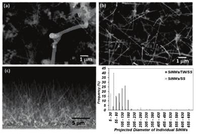
64 42
![selected area diffraction (SAD) pattern indicates that the SiNW is close the [112] zone axis of Si. The SiNW shown in Figure 2.3(b) is imaged using the g=111 reflection.](/docs-images/71/65930728/images/65-0.jpg "According to HRTEM in Figure 2.3(c), exposure to air after the growth leads to the formation of less than 5 nm SiO 2 on the surface of the SiNWs. Figures 2.3(d-f) show the TEM images of the 1Al/SiNWs.")
65 selected area diffraction (SAD) pattern indicates that the SiNW is close the [112] zone axis of Si. The SiNW shown in Figure 2.3(b) is imaged using the g=111 reflection. According to HRTEM in Figure 2.3(c), exposure to air after the growth leads to the formation of less than 5 nm SiO 2 on the surface of the SiNWs. Figures 2.3(d-f) show the TEM images of the 1Al/SiNWs. The spots observed in the SAD pattern are due to the Si single crystal. The dark field image is taken from the g=111 Si. The faint continuous ring in the diffraction pattern corresponds to Al. The dark field image in Figure 2.3(f) is imaged using a portion of this ring. As it is evident from this image, Al does not form a continuous layer on the SiNW surface. Figures 2.3(g-l) demonstrate the microstructures of the as prepared 3Al/SiNW and 13Al/SiNWs. The corresponding SAD patterns from both materials consist of spotty and ring patterns. The spots are due to the Si single crystal shown in the dark field micrograph in Figures 2.3(h) and 2.3(k) (taken from the g=111 Si reflection). The simulation of the observed ring pattern indicates that the rings correspond to Al. The dark field images shown in Figure 2.3(i) and 2.3(l) are imaged using a portion the 111 Al ring. It appears that the Al coating is not conformal around all of the SiNWs and the thickness of Al layer is different around each SiNW. This is more pronounced in the 13Al/SiNW (Figure 2.3(g)). It should be noted that the surface of SiNWs is smoother with thinner Al layer, since the grain size is smaller (Figure 2.3(f)), while thicker Al layer has the larger grain size (Figure 2.3(l)) leading to a rougher surface. Figure 2.2: SEM images of the (a) SiNWs/TiN, (b) 1Al/SiNWs, (c) 3Al/SiNWs, (d) 8Al/SiNWs, and (e) 13Al/SiNWs. 43
 (c) show TEM micrographs of the SiNW/TiN (a) bright field micrograph with corresponding indexed selected area diffraction (SAD) insert, (b) dark field micrograph, obtained using g ¼ 111Si with")
66 Figure 2.3: TEM micrographs of bare and coated SiNWs. (a) (c) show TEM micrographs of the SiNW/TiN (a) bright field micrograph with corresponding indexed selected area diffraction (SAD) insert, (b) dark field micrograph, obtained using g ¼ 111Si with the wire oriented near the 112 symmetric zone axis, (c) HRTEM image of the SiNW structure. Fig. 3 (d) (f) show 1Al/SiNW. (d) Bright field micrograph with corresponding indexed SAD insert, (e) dark field micrograph of the Si obtained using g ¼ 111Si. (f) Dark field micrograph, obtained using a portion the 111Al ring pattern. (g) (i) show 3Al/SiNW. (g) Bright field micrograph with corresponding indexed composite SAD insert, (h) dark field micrograph of the Si obtained using g ¼ 111Si. (i) Dark field micrograph, obtained using a portion of the 111Al ring pattern, highlighting the nanocrystalline grain size of Al. Fig. 3(j) (l) show 13Al/SiNW. j) Bright field micrograph with corresponding indexed composite SAD insert, (k) dark field micrograph of the Si obtained using g ¼ 111Si. (l) Dark field micrograph, obtained using a portion of the 111Al ring pattern, highlighting the much coarser albeit still nanocrystalline grain size of Al. 44
67 As mentioned before, TiN was used as one of the substrates to grow SiNWs on. Figure 2.4(a) clearly shows that TiN has a very low reactivity with respect to lithium-ion insertion, revealing lower storage capacity by more than an order of magnitude compared to SS (Figure 2.4(b)). Hence, it can protect the SS substrate from reaction with Li. It can be confirmed by the charge/discharge curves, since no distinct plateaus are observed on the charge/discharge curves of TiN. Therefore, the electrochemical charge/discharge response is entirely due to Al/SiNWs composites. For the SS spacer without TiN (Figure 3.4(b)) a sloped plateau centered around 0.9 V and 1.2 V for reduction and oxidation, respectively is observed indicating that the native oxide on SS does indeed reversibly react with Li. Figure 2.4: Galvanostatic discharge/charge curves of the (a) SS spacer coated with TiN layer and (b) SS spacer without any coating layer. Figure 2.5 shows the capacity data for the SiNWs/TiN as well as SiNWs/SS cycled between 0.01 to 2 V up to 50 cycles. The first discharge capacity for the SiNWs/SS was 3050 mah/g, which was lower compared to the SiNWs/TiN (3581 mah/g). The first coulombic 45
68 efficiency defined as CE = (delithiathion capacity/lithiation capacity) and the first discharge capacity loss were 84.3% and 14.5% for the SiNWs/SS, whereas they were 93.1% and 4% for the SiNWs/TiN, respectively. The subsequent capacity degradation rate on the other hand, is approximately the same for both SiNWs/TiN and SiNW/SS. Figure 2.5: Galvanostatic discharge/charge curve of the (a) SiNWs/TiN, (b) SiNWs/SS, and (c) discharge capacity retention of the SiNWs/TiN and SiNWs/SS at 0.1 C rate. After 50 cycles, the capacity is still ~75% of that in the second cycle. Another difference between SiNWs on TiN and SS is that for the latter, the growth temperature was lower which favors the formation of amorphous Si next to SiNWs. Before the onset of the long plateau at 0.1 V, there is a large, sloping plateau of ~600 mah/g (see Figure 2.6) which may be related to an amorphous Si fraction that is already present in as-grown SiNWs/SS. 46
69 Figure 2.6: First lithiation response of SiNWs/SS highlighting the contribution of amorphous Si. Figure 2.7 shows the XRD patterns of SiNWs/SS in the as-made condition, after lithiation to 0 V and delithiation to 2 V. For the as-made material, peaks of crystalline Si and the SS substrate are clearly visible. For the Au catalyst used for growing the nanowires, the (111), (200) and (220) reflections are visible at 38.2, 44.4 and 64.5 o, respectively. A trace amount of the FeSi 2 intermetallic is also present. After lithiation, all Si has transformed to crystalline Li 15 Si 4. Au also forms an intermetallic with Li with the exact same Li-content, Li 15 Au 4, which appears to be amorphous. In fact, it is this reaction of Li with gold that causes the small plateau at ~0.15 V in the delithiation curves of Figure 2.5(b). 33 The FeSi 2 phase remains inactive as was also observed in previous studies. 33 After delithiation to 2 V, all Si and Au have become amorphous and only the peaks from FeSi 2 and SS remain. The electrochemical response of the SiNWs/TiN, 3Al/SiNWs, 19Al/SiNWs and pure Al were investigated with cyclic voltammetry (CV) with a scan rate of 1 mv/s. The first ten scans are presented in Figure 2.8. For uncoated Si NWs in Figure 2.8(a), there is a reduction peak starting at a potential of about 0.3 V vs. Li/Li +, which becomes quite large at about 0.1 V. This peak is associated with the insertion of lithium ion into the Si NWs and the formation of Li x Si alloys. A double peak response is measured during lithium-ion extraction. This is consistent with previous experiments on micro-structured silicon anodes
70 Figure 2.7: XRD patterns of SiNWs/SS in as-made, lithiated and delithiated state. Figure 2.8: Cyclic voltammetry profiles of the (a) SiNWs/TiN, (b) 3Al/SiNWs, (c) 19Al/SiNWs, and (d) 50 nm of pure aluminum on TiN/SS substrate with the scan rate of 1 mvs -1. For 19Al/SiNWs in Figure 2.8(c), the first peak ascribed to Si at ~0.3 V is completely absent from the first two cycles. This means the large peak at ~0.6 V has to be ascribed to Al for 48
71 this material. This is supported by the data in Figure 2.8(d), where a pure 50 nm Al film shows its delithiation peak at the same potential around 0.6 V. The CV curves of the 3Al/SiNWs are almost the same as that of the bare SiNWs. Since the amount of Al is only about 0.01 mg for this sample, which is much less than that of the SiNWs (~0.33 mg) and the specific capacity of Al is, at only 993 mah/g (corresponding to LiAl formation) 47, 48, much lower than that of silicon (3590 mah/g for the formation of crystalline Li 15 Si 4 phase) 49, the reduction/oxidation peaks related to Al in 3Al/SiNWs will be too small to be distinguished in a CV curve. The magnitude of the current peaks increases with cycling due to the activation of more materials to react with lithium with each scan. It can also be referred to an improvement of the reaction kinetics during cycling by repeatedly insertion/extraction of lithium ions in which the conductivity may improve as a result of the lithium-doping or changes in geometry. 50 Galvanostatic charge/discharge experiments of the Al/SiNWs electrode with different Al weight percentages were carried out in the voltage range of V. Uncoated SiNWs/TiN electrode was also measured for comparison. Figures 2.9(a-f) show the discharge and charge capacity data for the electrodes in order of increasing Al wt%. The curves obtained during the first charge/discharge process for uncoated and coated SiNWs show a long voltage plateau located at around 0.1 V during lithiation, which is indicative of a two-phase region where crystalline silicon is being transformed into an amorphous lithium silicide, Li x Si. 51,52 This is analogous to the reduction peak observed in the CV experiment of SiNWs/TiN in Figure 2.8(a). The delithiation curves exhibit a single and flat plateau at about 0.4 V, which means that during lithiation the amorphous phase is transformed to crystalline Li 15 Si If crystalline Li 15 Si 4 is not formed during lithiation, there would be two sloping plateaus during the subsequent delithiation process. 53 The formation of this phase can also be confirmed by the specific capacity observed in the first lithiation process for SiNWs/TiN (Figure 2.9(a)). As could be seen, the first discharge capacity of SiNWs is 3581 mah/g close to the theoretical capacity of silicon (3590 mah/g), when crystalline Li 15 Si 4 is formed at full lithiation. 54 The amorphous material exhibits lower specific capacity of around 3000 mah/g (equivalent to 3.2 Li per Si). 52 Consequently, the delithiation curves show a plateau at about 0.4 V because of the two-phase reaction from crystalline Li 15 Si 4 to amorphous Li z Si phase, which is then followed by a solid-solution reaction from amorphous Li z Si to amorphous Si. 49
72 Figure 2.9: Galvanostatic discharge/charge curves of the (a) SiNWs/TiN, (b) 1Al/SiNWs, (c) 3Al/SiNWs, (d) 8Al/SiNWs, (e) 13Al/SiNWs, (f) 19Al/SiNWs, (g) first discharging, and (h) first charging cycle at 0.1 C rate. The contribution of Al to the electrochemical response is highlighted by arrows in Figure 2.9(h). There is a small plateau in the voltage profile of the Al/SiNWs at around 0.14 V (Figure 2.9(g)), which is most pronounced for the 19Al/SiNWs, which means it corresponds to the lithium insertion into Al. 55 The small magnitude of this plateau compared to the long plateau at 0.1 V confirms the small contribution of Al in electrochemical performance of SiNW electrode. This is in agreement with the CV curves in Figure 2.8. The Al lithiation is much less obvious for the materials with lower Al thickness in Figure 2.9(g) although for 13Al/SiNWs there is still a clear feature in the potential profile between 0.15 and 0.1 V. However, from the delithiation curves the presence of Al is more obvious. Figure 2.9(h) shows a magnification of the first delithiation cycle for all our materials. There is a small sloping plateau at approximately 0.5 V, indicated by the arrows, which diminishes continuously with decreasing Al thickness. 50
73 Table 2.1 summarizes the first discharge and charge capacities as well as the coulombic efficiencies of the SiNWs/TiN as well as Al/SiNWs. Compared with the SiNWs/TiN, Al/SiNWs electrodes show a reduced capacity. As mentioned before, lithium insertion in Al leads to the formation of LiAl with a maximum capacity of 993 mah/g on the first alloying with lithium 47, 56, which is much lower than that of silicon. Of all the materials that were tested, only the SiNWs/SS has a significantly lower coulombic efficiency in the first cycle. It should be noted that the CE in the first cycle is not significantly different between bare SiNWs on TiN and the Al-coated materials and is always between 92 and 94%, which, to the authors knowledge, are the highest first-cycle efficiencies ever reported. The fact that the presence and also the thickness of the coating do not significantly influence the initial coulombic efficiency is surprising. Previous studies on Cu and carbon-coated SiNWs showed a large influence of the coating and the coulombic efficiency was improved from 69.5 to 90.3% and 83.2%, respectively. 34, 41 Possible reasons for these discrepancies will be discussed later. Table 2.1: The capacity and coulombic efficiency of the SiNWs/TiN and Al/SiNWs electrodes in the first cycle Discharge Capacity Charge Capacity CE Sample (mah/g) (mah/g) (%) SiNWs/SS (0.1C rate) SiNWs/TiN (0.1C rate) Al/SiNWs (0.1C rate) Al/SiNWs (0.1C rate) Al/SiNWs (0.1C rate) Al/SiNWs (0.1C rate) Al/SiNWs (0.1C rate) Figures 2.10(a) and (b) show the cycle life of SiNWs/TiN and Al/SiNWs at 0.1 C rate. The first discharge capacity loss for both SiNWs/TiN and Al/SiNWs is around 4%. As can be seen, the 3Al/SiNWs and 8Al/SiNWs exhibit better cycling performance compared to the other Al thicknesses as well as the SiNWs/TiN. Both SiNWs/TiN and Al/SiNWs show a stable capacity up to 25 cycles after which it starts to drop with a higher rate for the 1Al/SiNWs as 51
74 well as SiNWs/TiN. The 3 wt.% Al coating layer has the best result on the cycling performance of the SiNWs. It gives a stable reversible capacity of approximately 1300 mah/g after 100 cycles, a capacity retention of about 40%, while the capacity of SiNWs/TiN decays rapidly to 1090 mah/g after 100 cycles (~30%). The biggest improvement is seen after 75 cycles where the bare and 3 wt.% coated SiNWs show 42% and 55% capacity retention, respectively. Thus, improvement of the cycling stability of SiNWs is observed after coating with Al for a certain range of wt.% Al/coating thicknesses. The 1Al/SiNWs degrades with the same rate that is observed in the SiNWs/TiN. For higher than 8wt.%Al, no additional decrease in the degradation rate is observed and only results in decrease of the total gravimetric capacity due to the high amount of Al. Coulombic efficiency versus cycle number is shown in Figure 2.10(c) for the SiNWs/TiN and Al/SiNWs. The initial coulombic efficiency of the SiNWs/TiN is almost the same as Al/SiNWs electrodes. The slight variations in the first cycle coulombic efficiency between the samples could be related to the difference in the surface area as the SEM images in Figure 2.2 showed that thicker Al coatings increase the surface roughness. After the first cycle, the coulombic efficiency is more stable for the 3Al/SiNWs and 8Al/SiNWs throughout cycling compared to all the other samples. Although 1Al/SiNWs initially shows the highest coulombic efficiency near 100%, it drops faster at higher cycles. On the other hand, when the Al coating is too thick, the coulombic efficiency is not as stable as 3Al/SiNWs and 8Al/SiNWs. It can also be seen in Figure 2.10 that the cycles where capacity degredation is fastest coincides with those where the coulombic efficiency is lowest, as would be expected. The dependence of discharge capacity versus cycle number for the 3Al/SiNWs at 0.2 C and 0.1 C rates is shown in Figure 2.11(a). The 0.2 C rate cycling shows slightly better cycle performance. The first coulombic efficiency is about 96% and the irreversible capacity is lower in the first cycle than that at 0.1 C rate. It can be due to the formation of less SEI layer and occurrence of the less side reactions with the electrolyte at higher charge/discharge rate since less time is spent at the potentials where these reactions occur. Moreover, the first charge curve shows sloping profile at 0.2 C rate, although there is still an indication of a plateau (Figure 2.11(b)). 52

75 Figure 2.10: (a) Cycle life, (b) discharge capacity retention, and (c) coulombic efficiency of the uncoated and aluminum-coated SiNWs/TiN at 0.1 C rate. At 0.1 C rate, the charge curve exhibits a single plateau at about 0.4 V, which is followed by an upwardly sloping region. As discussed earlier, if Li 15 Si 4 phase is formed during the lithiation, the subsequent charge curves include a plateau at about 0.4 V, since there is a twophase reaction from the crystalline to amorphous phase. It seems that the crystalline Li 15 Si 4 phase is only partially formed during charging at 0.2 C rate. The formation of the Li 15 Si 4 phase may be rate dependent. 33 It has been observed that amorphous silicon thin films can sustain high capacity even at high discharge rates with the good cyclability due to the facile lithium insertion and extraction into the single phase. Moreover, the volume expansion of amorphous 53
76 alloy as a result of the lithium insertion is known to be homogeneous without pulverization as it occurs in the crystalline materials. 57 Figure 2.11: (a) Discharge capacity retention, and (b) first charging cycle of the 3Al/SiNWs at 0.2 and 0.1 C rate. In order to determine whether the uncoated and coated SiNWs morphology changes after cycling, the cells were disassembled and the anode was further characterized. According to Figure 2.12(a), the uncoated SiNWs are completely disintegrated after 100 cycles, seem to have become porous, and extensive SEI formation is observed as flakes on the nanowires surface (see inset). Essentially the same picture is obtained for the 1Al/SiNWs where the microstructure strongly resembles that of uncoated SiNWs after cycling. Figures 2.12(c-e) show SEM images of the 3Al/SiNWs electrode, which had the best electrochemical cycling properties, at different cycle numbers and magnifications. The original morphology is apparently retained, although there appear to be minor modifications to the surface compared to the as-made material (see Figure 3.2) possibly due to the repeated lithiation/delithiation of the Al layer and/or minor SEI deposits after 30 cycles (Figure 2.12(c)). Most importantly, even after 100 cycles, there are still areas in the material where the nanowires have retained their original morphology. 54
 does show that closer to the substrate, there are areas where the nanowires have disintegrated to a similar extent as the uncoated and 1Al/SiNWs did.")
77 However, the higher magnification image in Figure 2.12(e) does show that closer to the substrate, there are areas where the nanowires have disintegrated to a similar extent as the uncoated and 1Al/SiNWs did. The same disintegration is observed for cycled 19Al/SiNWs in Figure 2.12(f). Similar to 3Al/SiNWs, there are areas where the original shape of the nanowires seems largely intact, but further down there is also evidence of disintegration. For this thicker Al coating, there is some evidence for agglomeration as larger particles are visible adjacent to the wires, indicating that thicker Al coatings are more vulnerable to agglomeration and breakup than thinner coatings. These images are in agreement with our cycling results in Figures 2.9 and The Al coating can slow down, but not prevent capacity degredation and this is probably due to the uncoated parts of the material disintegrating close to the substrate. This strongly suggests that if more uniform coating could be achieved, for instance by growing the nanowires with better vertical alignment, the cycling stability would be improved further. Figure 2.12: SEM images of the (a) bare SiNWs after 100 cycles, (b) 1Al/SiNWs after 100 cycles, 3Al/SiNWs after (c) 30, (d) and (e) 100 cycles, and (f) 19Al/ SiNWs after 55 cycles. Figure 2.13 shows TEM images of 1Al/SiNWs, 3Al/SiNWs and 19Al/SiNWs after 100 cycles in the delithiated state. In Figure 2.13(a) and (b), a disintegrated 1Al/SiNW is shown. The morphology is rather similar to that observed in the SEM images in Figure No SEI layer that was stable under the electron beam was observed. Figures 2.13(c-e) show TEM images of nanowires from the 3Al/SiNWs material. In this particular image, the Al coating seems to have peeled off from the NW s surface and has been replaced by an amorphous SEI layer that was stable 55

78 under the electron beam. This means it likely consists of inorganic compounds such as LiF and Li 2 CO 3. The outer part of this layer was observed to rapidly decompose under the TEM electron beam, indicating that the outer part had high organic content. The SiNW itself has also become amorphous as the SAD pattern and HRTEM image in Figure 2.13(c) and (e), respectively, show. The SAD pattern shows diffuse rings representative of an amorphous phase. For a different part of the same sample, presence of metallic Al on the surface could be confirmed by the simulation of the electron diffraction pattern shown in Figure 2.13(f). The dark field micrograph in Figure 2.13(g) is imaged by using a portion of the 111 Al ring. Figure 2.13(h) and (i) illustrate one of the particles on or adjacent to the 19Al/SiNWs in Figure 2.12f. As could be seen from the dark field image (Figure 2.13(i)) which has been taken from the g=200 Al reflection, the particles mostly consist of Al which has peeled off the SiNW. Figure 2.13: (a) and (b) show 1Al/SiNW. (a) bright field micrograph with corresponding SAD insert, (b) dark field micrograph taken from a portion of the 111Al ring. Fig. 2.13(c) (g) show TEM micrographs of the 3Al/SiNW. (c) and (f) bright field micrograph with corresponding SAD insert, (d) dark field micrograph obtained using a portion of amorphous Si ring, (e) HRTEMimage of the SiNW structure, (g) dark field micrograph obtained using a portion of amorphous 111Al ring. Fig. 11 (h) and (i) show a particle adjacent to the 19Al/SiNWs. (h) bright field micrograph with corresponding indexed selected area diffraction (SAD) insert, (i) dark field micrograph, obtained using g ¼ 200Al reflection. 56
79 From the results presented so far we observe that 1): the initial coulombic efficiency, as well as the total capacity, is significantly higher for SiNWs grown on TiN than on SS and higher than previous reports on SiNWs. 2): after the first cycle, SiNWs on TiN and on SS degrade at approximately the same rate 3): sufficiently thick Al layers can mechanically stabilize the coated parts of the SiNWs and prevent them from pulverizing. 4): there is an optimum in the Al thickness where capacity degredation is slowed down but not prevented. A coulombic efficiency < 100% can be due to SEI formation, irreversible reactions such as reduction of SiO 2 and loss of active material during lithiation due to pulverization. From XPS measurements by Chan et al, SiO 2 reduction was found to take place at potentials above 0.5 V 58. It was found in Figure 2.9(g) that the capacities in the first cycle even down to a potential of 0.25 V are lower than 55 mah/g for all our materials, which shows that the contribution of the native oxide layer is small. Besides Si, the Al probably has a (amorphous) native oxide layer as well. However, for all Al coated samples we found evidence for metallic Al in both as-made and cycled states. Furthermore, a native oxide layer on Al can be transformed upon lithiation to a ternary Li-Al-O glassy phase that is an excellent Li-ion conductor 59. Therefore, partial oxidation of the Al surface is not expected to have a negative impact on the electrochemical properties of our SiNWs and from Figures 2.9 and 2.10 we indeed see no evidence for this. Incidentally, a fully oxidized Al shell in the form of Al 2 O 3 has a negative influence on the cycling performance of SiNWs (see Figure 2.14). Figure 2.14: Cycling stability of bare SiNWs, 3Al/SiNWs and SiNWs coated with 4 wt.% Al2O3 deposited by ALD. 57

80 Because of the high volumetric expansion of Si upon lithiation, the SiNWs may be very sensitive to pulverization/cracking and contact loss with the substrate at the base. An earlier study by Ryu et al. showed that thick nanowires can disintegrate during the first lithiation. 60 Based on numerical modeling, combined with ex-situ TEM observations, a critical diameter for fracture and pulverization was established in the range of 220 ~ 260 nm. The observed difference in total capacity and coulombic efficiency between SiNWs grown on TiN and SS, 3581 vs mah/g and 93.1 vs. 84.3%, respectively, may therefore be explained by differences in pulverization resistance. From the SEM images and size distributions in Figure 2.1, SiNWs/SS was observed to have a higher number of very thick nanowires and a significant fraction is above the critical size of around 250 nm. Figure 2.15(a-e) depicts a series of SEM images of as-grown SiNWs/SS (a and b) and after one lithiation/delithiation cycle (c-e). Initially, some very thick nanowires are observed, the same as in Figure 2.1(a) and 2.15(a), but after only one cycle, no thick nanowires are observed either near the substrate (c and d) or in a top-down view (e). This is a strong indication that SiNWs above a critical size pulverize in the first lithiation cycle, leading to the relatively low coulombic efficiency that we observed. Figure 2.15: SEM micrographs of SiNWs/SS electrode (a) and (b) as-synthesized, (c) (e) after the first cycle. (c) and (d) near the SS substrate, (e) top-down view. 58

81 Another contributing factor to capacity loss could be detachment of the SiNWs from the substrate, either abruptly in the first cycle or gradually in the course of cycling. It has been observed that FeSi alloys, which are formed at the interface between SS and SiNWs during the high temperature SiNW growth, can react with Li during electrochemical cycling. 61 The cycling stability of FeSi 2 powder turned out to be extremely poor, indicating the material is readily pulverized. Although formation of a small amount of FeSi 2 was confirmed by XRD (see Figure 2.7) it was still present in the lithiated and delithiated states, making it unlikely that Li reacting with iron silicides contributed to the first cycle capacity loss in SiNWs/SS. The other side reaction that is unique to the SS substrates is the conversion of Cr 2 O 3 to Cr and Li 2 O. However, given that this reaction is reversible (see Figure 2.4), one would expect the effects to be visible throughout the course of cycling and not only in the first cycle, but the degredation rates of SiNWs/SS and SiNWs/TiN were found to be similar in Figure 3.5. Although the SS substrate does show signs of surface damage in some places after removal of the SiNWs after 1 cycle (see Figure 2.16), the role of Cr 2 O 3 in capacity degradation seems minor. Figure 2.16: Surface of the stainless steel substrate after polishing steps (a) and after lithiation/delithiation cycle and removal of the Si nanowires (b). Our third general observation relates to the observed mechanical stability of the nanowires during cycling. Radial expansion of SiNWs was found to be very large and highly anisotropic in in-situ TEM studies. 62 Upon lithiation, the initially cylindrical shape of the nanowires was transformed into a dumbbell-shape which could lead to rupture of the nanowire through the middle, effectively cutting its size in half. This can explain the disintegration we observed for 59
82 the uncoated and 1Al-coated SiNWs in Figure 2.12 and However, despite this large anisotropic expansion upon lithiation, our results clearly indicate that a thick enough Al coating can maintain the mechanical integrity of the nanowires during prolonged cycling. This means the Al coating likely does modify the expansion, either directing it more in the axial direction rather than radial or making radial expansion more isotropic by exerting a compressive stress on the SiNW during lithiation. The 1Al-coating appears to be too thin, and thus too vulnerable to rupture, to have this strong stabilizing effect. A compressive stress on the SiNWs during lithiation could also help to keep SiNWs with near-critical diameters intact. Applying a 3 and 8 wt.% Al coating to SiNWs/SS resulted in improvement from 84.3 for bare SiNWs/SS to 88.7% and 91.5% coulombic efficiency, respectively, in the first cycle (see Figure 2.17) lending support to this hypothesis. This may also explain why the Al coating had so little influence on the coulombic efficiency in the first cycle for SiNWs on TiN. These had a relatively narrow size distribution around 100 nm and will not have any problems with pulverization related to their size. However, Chen et al. reported substantial improvement in coulombic efficiency in the first cycle for nanowires with diameters similar to ours; approximately 100 nm. 34, 41 However, a very high mass-loading, 0.6 mg/cm 2 compared to 0.18 mg/cm 2 for the present study, and long growth time (2 h) was reported, which means the nanowires should be very long. This may increase the mechanical vulnerability of the nanowires causing the coating layer to have a beneficial effect, despite the sufficiently small diameter. A way to test this hypothesis further would be to grow well-aligned SiNWs with narrow size distributions but different average diameters by controlling the size of the Au catalyst particles on TiN. A possible way to achieve this would be to adjust the Au layer thickness, as was recently demonstrated for Ni particles on SiO Although 3Al/SiNWs and 8Al/SiNWs degrade more slowly than the other samples, all the materials eventually do degrade to what appears to be a steady-state capacity that is between 28 and 38% of the initial capacity (see Figure 2.10(b)). Loss of active material should be evident as an increase in internal resistance of the electrodes. To investigate this, we performed electrochemical impedance spectroscopy on bare and coated SiNWs in their as-made and cycled states. The results are shown in Figure 2.18 in the form of a Nyquist plot. Another possibility is that over the course of cycling, more and more SiNWs gradually detach from the TiN substrate. The spectra are composed of one semicircular arc at high frequencies indicative of a charge 60
83 transfer reaction where the diameter of the semicircle equals the charge transfer resistance (R ct ), followed by a nearly straight line at 45 o or higher angle with respect to the real axis at lower frequencies. The shift of the impedance spectra along the real axis is approximately 3 Ohm for all samples. This value is the sum of all electrical resistances within the electrodes, which includes the contact resistance between the current collector and the SiNWs. The bare SiNWs displays a very large semicircle, indicative of high charge transfer resistance that is likely due to the presence of native oxide. The xal/sinws have significantly lower charge transfer resistance, similar to what was found for Cu and carbon coatings 34, 41 further highlighting the beneficial effects of the Al coating. Figure 2.17: First and second cycles for SiNWs/SS (a) and 3Al/SiNWs/SS and 8Al/SiNWs/SS (b). For all electrodes, there was an increase in the electrical resistance of approximately a factor of 4, which is indicative of contact loss between the active material, i.e. the SiNWs, and the current collector/substrate. Nanowire detachment from the substrate will reduce the number of conductive pathways for electrons and increase reaction resistances in the electrode. In principle, this should lead to an increase in R ct by a similar factor, but the effect is much smaller, 61
84 probably due to the presence of native oxides in the as-made materials that are reduced in the first lithiation cycle. As a result, for the bare SiNWs the charge transfer resistance is even lower in the cycled state than in the as-made state. R ct is significantly higher for bare SiNWs and 13Al/SiNWs compared to 3Al and 1Al, which reflects a higher tendency for SEI formation for the uncoated SiNWs and for thick Al coatings sensitive to agglomeration and detachment from the nanowire surface. Figure 2.18: Impedance spectra of uncoated and Al coated SiNWs on TiN/SS substrate (a) assynthesized, (b) after 100 cycles. The most important benefit of the Al coating is the prevention of pulverization. The coated parts of the nanowires were clearly protected from degredation as seen from the SEM images in Figure However, progressive pulverization of the parts near the substrate still leads to capacity degredation down to 28 to 38% of the original capacity, corresponding to between 785 (19Al/SiNWs) and 1292 mah/g (3Al/SiNWs). However, the capacities seem to stabilize as the coulombic efficiency increases again in late stages of cycling, which means a certain fraction of the nanowires will remain attached to the substrate and remain electrochemically active. Furthermore, the material with optimum coating thickness, 3Al/SiNWs, seems to stabilize at a 62
85 higher capacity than bare nanowires. This strongly suggests that the Al coating also has a positive influence on wire attachment to the substrate and that if coverage of the nanowires by the coating layer can be improved, the beneficial effects of the Al coating will be more pronounced. This can be achieved by growing the nanowires with a lower density and better vertical alignment, which may be possible by adjusting the Au layer thickness, in order to reduce shadowing effects during Al deposition. Also, transferring our SiNW growth process with TiN interlayers onto commercially available copper foils that are commonly used as current collectors in Li-ion batteries should be undertaken to bring these materials closer to practical application. 2.4 Conclusions We compared the electrochemical performance of SiNWs grown on TiN and SS and investigated the effects of Al coating. Only the SiNWs grown on SS had a significant fraction of nanowires above a critical diameter (~250 nm) that pulverize upon lithiation leading to lower initial coulombic efficiency for SiNW/SS, 84.3%, compared to SiNW/TiN, 93.1% when cycling between 0.01 and 2V vs. Li/Li + at 0.1C rate. Such small amount of irreversible capacity loss for bare SiNWs during the first cycle has never been observed in previous studies. We therefore conclude that the size distribution has a large influence on the stability and should be optimized, preferably with an average diameter around 100 nm or less. Coating with Al showed no additional benefit to the initial coulombic efficiency, but improved the capacity retention when the thickness was within an optimum range between 3 and 8 wt.% by helping to maintain the mechanical integrity of the nanowires. When the coating was too thin, it was still too vulnerable to fracture, when it was too thick, it tended to agglomerate and peel off the surface of the nanowires. The biggest improvement was seen after 75 cycles where bare SiNWs retained 42% of their original capacity and 3Al/SiNWs 55%. After 100 cycles, the materials retained between 28 (19Al/SiNWs) and 38% (3Al/SiNWs) of their original capacity which showed Al coating slows down the capacity degredation but does not prevent it. This means the nanowires still disintegrate and detach from the substrate at their base. Nevertheless, the higher steady-state capacity after 100 cycles for 3Al/SiNWs suggests that Al coating also helps maintain contact with the substrate. 63
86 In summary, we have shown that SiNWs with an Al shell with an optimized thickness are promising anode materials for rechargeable lithium-ion batteries. Future research should concentrate on improving the coverage of the SiNWs by the coating layer and further investigating the effects of the nanowire diameter and density and finding ways to control them. 64
87 2.5 References 1. S. A. Freunberger, Y. Chen, Z. Peng, J.M. Griffin, L. J. Hardwick, F. Barde, P. Novak and P. G. Bruce, Journal of the American Chemical Society, 2011, 133, R. Marom, S. F. Amalraj, N. Leifer, D. Jacob and D. Aurbach, J. Mater. Chem., 2010, 21, J. S. Thorne, J. R. Dahn, M. N. Obrovac and R. A. Dunlap, J. Alloys and Comp., 2011, 509, A. Yu, H. W. Park, A. Davies, D. C. Higgins, Z. Chen and X. Xiao, J. Phys. Chem. Lett., 2011, 2, J. Danet, T. Brousse, K. Rasim and D. Guyomard, Phys. Chem. Chem. Phys., 2010, 12, S. Bijani, M. Gabas, G. Subias, J. Garcia, L. Sanchez, J. Morales, L. Martinez and J. R. Ramos-Barrado, J. Mater. Chem., 2011, 21, A.M.A. Hashem, A.E. Abdel-Ghany, A.E. Eid, J. Trottier, K. Zaghib, A. Mauger, C.M. Julien, J. Power Sources, 2011, 196, C. Martin, O. Crosnier, R. Retoux, D. Belanger, D. M. Schleich and T. Brousse, Adv. Funct. Mater., 2011, 21, J. Danet, T. Brousse, K. Rasim, D. Guyomard and P. Moreau, Phys. Chem. Chem. Phys., 2010, 12, V. L. Chevrier, J. W. Zwanziger and J. R. Dahn, J. Alloys and Comp., 2010, 496, D. Mazouzi, B. Lestriez, L. Roue, D. Guyomard, Electrochem. And Solid-State Lett., 2009, 12, A215-A T. D. Hatchard and J. R. Dahn, J. Electrochem. Soci., 2004, 151, A838-A V. L. Chevrier, J. W. Zwanziger and J. R. Dahn, Can. J. Phys., 2009, 87, S. H. Ng, J. Wang, D. Wexler, K. Konstantinov, Z. P. Guo, and H. K. Liu, Angew. Chem. Int. Ed., 2006, 45, T. Zhang, J. Gao, L. J. Fu, L. C. Yang, Y. P. Wu and H. Q. Wu., J. Mater. Chem., 2007, 17, J. Guo, X. Chen and C. Wang, J. Mater. Chem., 2010, 20, D. Larcher, S. Beattie, M. Morcrette, K. Edstroem, J. C. Jumas and J. M. Tarascon, J. Mater. Chem., 2007, 17,
88 18. S. Ohara, J. J. Suzuki, K. Sekine and T. Takamura, Electrochemistry, 2003, 71, Y. Xu, G. Yin, Y. Ma, P. Zuo and X. Cheng, J. Mater. Chem., 2010, 20, L. Ji and X. Zhang, Electrochem. Commun., 2009, 11, M. H. Park, M. G. Kim, J. Joo, K. Kim, J. Kim, S. Ahn, Y. Cui and J. Cho, Nano Lett., 2009, 9, T. Song, J. L. Xia, J. H. Lee, D. H. Lee, M. S. Kwon, J. M. Choi, J. Wu, S. K. Doo, H. Chang, W. Il Park, D. S. Zang, H. Kim, Y. G. Huang, K. C. Hwang, J. A. Rogers and U. Paik, Nano Lett., 2010, 10, J. R. Szczech and S. Jin, Energy Environ. Sci., 2011, 4, Y. Kumai, H. Kadoura, E. Sudo, M. Iwaki, H. Okamoto, N. Sugiyama and H. Nakano, J. Mater. Chem., 2011, 21, J. S. Xue, K. Myrtle and J. R. Dahn, J. Electrochem. Soc., 1995, 142, K. Wang, X. He, L. Wang, J. Ren, C. Jiang, C. Wan, Solid State Ionics, 2007, 178, N. S. Choi, Y. Yao, Y. Cui and J. Cho, J. Mater. Chem., 2011, 21, J. L. Gómez-Cámer, J. Morales and L. Sánchez, J. Mater. Chem., 2011, 21, M. Holzapfel, H. Buqa, L. J. Hardwick, M. Hahn, A. Würsig, W. Scheifele, P. Novák, R. Kötz, C. Veit and F. M. Petrat, Electrochim. Acta, 2006, 52, B. Laїk, L. Eude and J. P. Pereira-Ramos, Electrochim. Acta, 2008, 53, T. Song, D. H. Lee, M. S. Kwon, J. M. Choi, H. Han, S. G. Doo, H. Chang, W. Park, W. Sigmund, H. Hansu Kim and U. Paik, J. Mater. Chem., 2011, 21, B. Laïk, D. Ung, A. Caillard, C.S. Cojocaru, D. Pribat and J.P. Pereira-Ramos, J. Solid State Electrochem., 2010, 14, C. K. Chan, R. Ruffo, S. S. Hong, R.A. Huggins and Y. Cui, J. Power Sources, 2009,189, H. Chen, Y. Xiao, L. Wang and Y. Yang, J. of Power Sources, 2011, 196, L. Hu, H Wu, S. Hong, L. Cui, J. R. McDonough, S. Bohy and Y. Cui, Chem. Commun., 2011, 47, T. Stephenson, A. Kubis, M. Derakhshesh, M. Hazelton, C. Holt, P. Eaton, B. Newman, A. Hoff, M. Gray and D. Mitlin, Energy & Fuels, 2011, 25,
89 37. S. Grugeon, S. Laruelle, L. Dupont, F. Chevallier, P. L. Taberna, P. Simon, L. Gireaud, S. Lascaud, E. Vidal, B. Yrieix and J-M. Tarascon, Chem. Mater., 2005, 17, L. Dupont, S. Laruelle, S. Grugeon, C. Dickinson, W. Zhou and J-M. Tarascon, J. Power Sources, 2008, 175, L. Dupont, S. Grugeon, S. Laruelle and J-M. Tarascon, J. Power Sources, 2007, 164, L.Q. Zhang, X. H. Liu, Y. Liu, S. Huang, T. Zhu, L. Gui, S.X. Mao, Z. Z. Ye, C. M. Wang, J. P. Sullivan and J. Y. Huang, ACS Nano, 2011, 5, and references therein. 41. H. Chen, Z. Dong, Y. Fu, Y. Yang, J. Solid State Electrochem., 2010, 14, K. Xu and A. Cresce, J. Mater. Chem., 2011, 21, Y. Yu, L. Gu, C. Zhu, S. Tsukimoto, P. A. van Aken and J. Maier, Adv. Mater., 2010, 22, D. Favez, L. Deillon, J.-D. Wagnière, M. Rappaz, Acta Mater., 2011, 59, C. Ophus, T. Ewalds, E. Luber, D. Mitlin, Acta Mater., 2010, 58, M. Green, E. Fielder, B. Scrosati, M. Wachtler and J. S. Moreno, Electrochem. Solid-State Lett., 2003, 6, A75-A M. D. Fleischauer, M. N. Obrovac, J. D. McGraw, R. A. Dunlap, J. M. Topple and J. R. Dahn, J. Electrochem. Soci., 2006, 153, A484-A D. Larcher, S. Beattie, M. Morcrette, K. EdstrÖm, J.C. Jumas and J. M. Tarascon, J. Mater. Chem., 2007, 17, M. D. Fleischauer, J. Li, and M. J. Brett, J. Electrochem. Soci., 2009, 156, A33-A G.L. Miller and W.A. Orr, Appl. Phys. Lett., 1980, 37, V. L. Chevrier, J. W. Zwanziger and J. R. Dahn, Can. J. Phys., 2009, 87, J. Li, A. Smith, R. J. Sanderson, T. D. Hatchard, R. A. Dunlap and J. R. Dahn, J. Electrochem. Soci., 2009, 156, A283-A L. Baggetto, R. A. H. Niessen, F. Roozeboom, P. H. L. Notten, Adv. Funct. Mater., 2008, 18, M. D. Fleischauer, J. Li, and M. J. Brett, J. Electrochem. Soci., 2009, 156, A33-A R. Krishnan, T. M. Lu and N. Koratkar, Nano Letters, 2011, 11,
90 56. C. Y. Wang, Y. S. Meng, G. Ceder and Y. Li, J. Electrochem. Soci., 2008, 155, A615-A L. Y. Beaulieu, T. D. Hatchard, A. Bonakdarpour, M. D. Fleischauer, J. R. Dahn, J. Electrochem. Soci., 2003, 150, A1457-A C.K. Chan, R. Ruffo, S. S. Hong and Y. Cui., J. Power Sources, 2009, 189, Y. Liu, N. S. Hudak, D. L. Huber, S. J. Limmer, J. P. Sullivan and J.Y. Huang, Nano Letters, 2011, 11, I. Ryu, J. W. Choi, Y. Cui and W. D. Nix, J. Mech. Phys. Solid, 2011, 59, N. Jayaprakash, N. Kalaiselvi, C. H. Doh, Intermetallics, 2007, 15, X. H. Liu, J. Y. Huang, Energy Environ. Sci., 2011, 4, E. J. Luber, B. C. Olsen, C. Ophus, D. Mitlin, Phys. Rev. B, 2010, 82,
91 3 ALD TiO 2 coated Silicon Nanowires for Lithium Ion Battery Anodes with enhanced Cycling Stability and Coulombic Efficiency Material in this chapter has been published in: E. Memarzadeh Lotfabad, P.Kalisvaart, K. Cui, A. Kohandehghan, M. Kupsta, B. Olsen, and D. Mitlin, Phys. Chem. Chem. Phys., 2013, 15, Introduction Li-ion batteries (LIBs) are currently the most important energy storage device for a wide variety of applications such as cell phones, laptops and other portable electronics 1-6. However, to meet the more demanding applications such as powering electrical vehicles, LIBs with higher energy density, longer cycle life, and faster discharge/charge rate than the existing ones are required Silicon is a promising anode material for LIBs owing to its large charge storage capacity of 3590 mah/g, corresponding to Li 15 Si 4, which is ten times higher than graphite (372 mah/g). The main drawback of silicon is its large volume expansion/contraction (~300%) upon alloying/dealloying with lithium, resulting in high mechanical stress, pulverization and loss of electronic contact leading to severe capacity degradation In addressing this problem, several approaches have been tried to enhance the cycling performance of Si anodes in LIBs. Among them, Si-based nanostructures including nanoparticles, 16,17 thin films, 18,19 nanowires, 12,20-22 and nanotubes 23,24 have attracted the most attention. Silicon nanowires (SiNWs) can accommodate the generated volumetric change anisotropically in both longitudinal and radial directions. Furthermore, anchored SiNWs on a conductive, possible flexible, substrate have no need of binder and conductive additives, potentially increasing the capacity of a full cell The high specific surface area of nanowires is both an advantage and a disadvantage. On 69
92 the one hand they provide a large area available for charge transfer reactions and their small diameter keeps Li diffusion distances short. On the other hand, the electrolyte solvents are thermodynamically unstable below 1.5 V vs. Li/Li + and the decomposition products immobilize part of the lithium in the battery in the so-called solid-electrolyte interphase (SEI). SEI formation is generally irreversible and a material with higher surface area will therefore cause higher irreversible charge losses. Furthermore, the high volume expansion of Si will continuously fracture the SEI during lithiation, exposing fresh Si to the electrolyte. This will increase the amount of SEI with each cycle, as well as increase the charge transfer and diffusion resistances. 28,29 Thus, researchers have been seeking ways to modify the surface of the electrodes to make the material less reactive with the electrolyte. Deposition of coatings onto silicon nanowires presents some challenges. They are usually grown using an Au-catalysed vapour-liquid-solid chemical vapour deposition process which produces poorly aligned nanowire forests. Highly directional deposition methods such as sputtering or thermal evaporation will result in incomplete coverage of the nanowires because of shadowing effects. Carbon, 30 copper, 31 and aluminium 22 coating of SiNWs using these methods have therefore had only limited success in improving the performance, although there is a marked improvement in the mechanical stability of the parts of the nanowires that do get conformally coated. 22, 32 Capacity degradation was slowed down, but not prevented, for SiNWs coated with 3-8 wt.% of Al, probably because the uncoated parts, near the nanowire base, are still subject to the same degradation mechanisms as bare SiNWs such as excessive SEI formation, agglomeration and delamination from the substrate. 33 Atomic layer deposition (ALD) is a method capable of producing conformal coatings on substrates of any size or shape with very precise control over the coating thickness. 11 Deposition of a continuous layer inside etched features (trenches) with aspect ratio as high as 1:20 has been achieved. 34 Conversely, conformal coating on nanopillars made of Al has also been demonstrated using ALD. 35 However, to date, ALD has not been employed to coat silicon nanowires, despite its potential to achieve complete coverage and thus markedly improve upon the performance of sputter or evaporation-coated SiNWs, if a suitable coating material can be selected. TiO 2 has been studied extensively as an anode material for LIBs in its own right Its 70
93 volume expansion upon lithiation according to: xli xe TiO2 LixTiO 2 (4.1) is less than 4%, which means its cycle life is excellent in general and the low expansion may be beneficial for adhesion of the coating to the underlying Si nanowire. Diffusion of lithium ions is found to be higher in a TiO 2 -Si composite than in bare silicon. 43 Furthermore, x is usually found to be 0.55 for anatase but can be close to 1 for amorphous TiO 2 and for very small anatase particles, turning the material from an insulator (bandgap ~3.5 ev) into an electronic conductor. Thus, TiO 2 coating on SiNWs is potentially beneficial for both structural integrity as well as the rate capability of the composite. As mentioned before, an important purpose of the coating is to make the Si less reactive with the electrolyte. TiO 2 is usually tested between 1 and 3 V vs. Li/Li + and, as a result, little is known about the reactivity of TiO 2 with the electrolyte at low potentials. It was found that the cycling stability of TiO 2 is not affected by extending the potential range down to 0.1 V and that the SEI formed on TiO 2 is thermally more stable than that on graphite, 44 which reacts with Li in the same potential range as Si (< 0.5 V vs. Li/Li + ). Therefore, applying TiO 2 coating onto SiNWs can improve the safety of the battery. In view of all the above, SiNWs coated with TiO 2 by ALD have great potential as a high performance Li-ion battery anode material. In the present paper, we study the influence of varying the ALD deposition parameters and TiO 2 layer thickness on the electrochemical properties and microstructure development of TiO 2 -coated SiNWs during galvanostatic cycling. A factor two improvement in capacity retention at 0.1 C and factor three improvement in rate capability at 5 C over a bare SiNW baseline is achieved. The reasons for the improved performance are found to be related to improved structural integrity, reduced agglomeration and passivation of the surface of SiNWs towards electrolyte decomposition for the optimal TiO 2 coating. 3.2 Experimental We prepared the SiNW electrodes by using a gold-catalyzed, vapour liquid solid growth on 316L stainless steel spacers (diameter 15.4 mm). In order to prevent penetration of Au into stainless steel, a Ti/TiN diffusion barrier with layer thicknesses of 50 and 200 nm, respectively, 71
94 was deposited onto the substrates using magnetron sputtering (Orion 8, AJA international). Base pressure was always below 5x10⁻⁸ mbar and the argon pressure during sputtering was 4 mtorr. For reactive sputtering of TiN, a N 2 :Ar ratio of 1:20 was used and the deposition temperature raised to 250 o C. 10 nm Au was deposited using RF magnetron sputtering at a power of 45 W at a rate of ~0.4 Å/s after cooling the substrate down to room-temperature. SiNWs were grown in a commercial Tystar CVD furnace. Prior to growth, the samples were annealed in vacuum for 30 minutes before introducing a SiH 4 :H 2 (ratio 1:4) mixture at a pressure of 100 Torr for a growth time of 2 minutes at the same temperature. Then, the substrates covered with SiNWs were placed in the ALD reactor. TiO 2 was deposited from titanium isopropoxides Ti(OCH(CH 3 ) 2 ) 4 as the titanium source and O 2 as the oxygen source. Argon was used as the carrier gas. We investigated the influence of the TiO 2 microstructure by varying the layer thickness and deposition temperature. Deposition of the coating was carried out at 200 o C and 300 o C and at 200 o C followed by annealing treatment at 600 C in vacuum for 1 h after deposition to get anatase TiO 2. The number of deposition/purge cycles required for 10 nm TiO 2 is 196 and 204 at 200 and 300 o C, respectively. The TiO 2 thicknesses used were 5, 10 and 15 nm, equivalent to mass loadings of ~0.05, 0.1 and 0.16 mg per sample, respectively. For an average mass of ~0.35 mg Si per sample, this corresponds to 12, 22 and 31 wt% TiO 2 in the TiO 2 /SiNWs nanocomposite, respectively. For the remainder of the manuscript the samples will be referred to as (x)tio 2 -y(a)/sinws, i.e. silicon nanowires coated with x nm TiO 2 at an ALD deposition temperature of y C, where (A) indicates post-deposition annealing treatment. In order to separately investigate the electrochemical properties of the coatings, 10 nm planar films on stainless steel spacers including the Ti/TiN barrier layer were deposited under identical conditions. The mass loading of TiO 2 on (10)TiO 2-200/SiNWs is equivalent to a 120 nm thick planar film, which means the SiNWs have approximately 12 times more surface area in contact with the electrolyte than a planar Si film. 316 stainless steel-cr2032 button half-cells using the TiO 2 /SiNW working electrodes and Li foil as counter electrodes were assembled in a glovebox filled with Ar with less than 0.2 ppm oxygen and moisture contaminations. A polyethylene (MTI technologies) separator (porosity of 36 44% and 0.03 µm pore size) soaked with a liquid electrolyte of 1 M LiPF 6 dissolved in a 1:1:1 volume ratio of ethylene carbonate (EC): dimethyl carbonate (DMC): diethylcarbonate (DEC) organic solvents was placed between the electrode and the lithium in the cell. The cells 72
95 were galvanostatically charged and discharged on a computer controlled BT2000 Arbin potentiostat between 0.01 and 2 V (vs. Li/Li + ) at various currents. Cyclic voltammetry (CV) was carried out using Versa STAT 3 potentiostat at 1 mv/s scan rate for SiNWs based anode materials and 0.2 mv/s for thin film materials in two different potential ranges ( V and 1-3 V (vs. Li/Li + )). Electrochemical impedance spectroscopy (EIS) measurements were measured using Versa STAT3 frequency response analyser FRA) by applying an AC voltage of 10 mv amplitude over a frequency range of 0.01 Hz to 1 MHz. After electrochemical testing, the coin cells were disassembled and the samples were rinsed thoroughly with acetonitrile and kept overnight in the glove box to remove the excess electrolyte. To characterize the morphology of the as-prepared and cycled samples, we used field emission scanning electron microscopy (FE-SEM) (Hitachi S-4800) and transmission electron microscopy (TEM) (JEOL 2010, 200 kv). Electron energy loss spectroscopy (EELS) analysis was conducted using a JEOL 2200FS TEM operated at 200 kv in a scanning TEM (STEM) mode with a nominal analytical beam size of 0.5 nm. High angle annular dark field (HAADF) images were recorded simultaneously with the EELS analysis. Compositional mapping was achieved with an in-column Ω filter. The software employed for signal collection and data extraction from EELS spectra was Digital Micrograph (Gatan, Inc.). The data extraction was performed by following the standard procedure of pre-edge background subtraction and integration on the edge. 45 Low-loss plasmon peaks at ev have been used for EELS mapping of Li-K. We mapped Si, C, Ti, and O elements by integrating over core loss edges of Si-L, C-K, Ti-L, and O-K at ~ , , , and ev, respectively. Cross-sectional samples of cycled materials were obtained using a Hitachi NB5000 dual beam FIB/SEM. X-ray photoelectron spectroscopy (XPS) measurements were performed on an ULTRA (Kratos Analytical) spectrometer using monochromatic Al-K α radiation (hν= ev) run at 210 W. Data collection was conducted under ultrahigh vacuum (10-9 Torr) from an area of μm 2. Spectra were collected with an energy window of 20 ev. A charge neutralizer was used to compensate for charging effects. The binding energy scale was calibrated from the universal hydrocarbon contamination using the C1s peak at ev. The XPS data were analyzed using CasaXPS software. Background subtraction was done using a 73
.")
96 nonlinear Shirley-type background model. 3.3 Results and Discussion SEM and TEM micrographs of as-made, VLS grown SiNWs coated with 10 nm of TiO 2 by ALD are presented in Figure 3.1 and nm was found to be the optimum coating thickness with regard to capacity and cycling stability (see Figure 3.3). All results presented hereafter were obtained with this coating thickness and it will therefore not be explicitly indicated anymore. The electrodes will be denoted as TiO 2 -y/sinws, where y is the ALD deposition temperature in o C, from here on. The SAD patterns of TiO 2-200/SiNWs and TiO 2-300/SiNWs consist of an overlay of a single crystal spot pattern of Si and a diffuse halo around the primary beam associated with amorphous TiO 2. For TiO 2-200(A)/SiNWs (A=annealing at 600 o C for 1 h), a second spot pattern belonging to anatase TiO 2 appears besides that of Si. Figure 3.1: SEM images of (a) SiNWs, (b) (10)TiO 2-200/SiNWs, (c) (10)TiO 2-300/SiNWs, (d) (10)TiO 2-200(A)/SiNWs. 74
 Bright field micrograph, (b) corresponding indexed selected area diffraction (SAD), (c) dark field micrograph obtained using a portion of the diffuse halo of amorphous TiO 2 between the primary")
97 Figure 3.2: TEM micrographs of TiO 2 coated SiNWs. (a)-(d): (10)TiO 2-200/SiNWs. (a) Bright field micrograph, (b) corresponding indexed selected area diffraction (SAD), (c) dark field micrograph obtained using a portion of the diffuse halo of amorphous TiO 2 between the primary beam and the first set of Bragg reflections of Si, (d) dark field micrograph of the Si obtained using g =111 Si with the wire oriented near the 112 symmetric zone axis, (e) (h): (10)TiO 2-300/SiNWs. (e) Bright field micrograph, (f) corresponding indexed SAD, (g) Dark field micrograph obtained using a portion of the diffuse halo of amorphous TiO 2 between the primary beam and the first set of Bragg reflections of Si, (h) dark field micrograph of the Si obtained using g=111 Si. (i) (l): (10)TiO 2-200(A)/SiNWs. (j) Bright field micrograph, (j) corresponding indexed SAD showing the 011, 020 and 024 diffraction spots of anatase TiO 2, (k) dark field micrograph, obtained using g=011 TiO2, (l) dark field micrograph of the Si obtained using g =111 Si. 75
98 76
, (d) and (g) are magnified by a factor 3 in (b), (e) and (h) which clearly show the lattice fringes for Si and, in the case of (10)TiO 2-200(A)/SiNWs,")
99 Figure 3.4: HRTEM images including fourier transforms (left and middle) and EELS maps (right) of (10)TiO 2-200/SiNWs, (a)-(c), (10)TiO 2-300/SiNWs (d)-(f), and (10)TiO 2-200(A)/SiNWs, (g)-(i). The areas delineated by the rectangles in (a), (d) and (g) are magnified by a factor 3 in (b), (e) and (h) which clearly show the lattice fringes for Si and, in the case of (10)TiO 2-200(A)/SiNWs, anatase TiO 2. The double-headed arrows in (a), (d) and (g) are the same length as the 10 nm scale bar. The HRTEM images and EELS maps show that the coating is at its nominal thickness. XPS spectra for the as-made materials (see Figure 3.5) show native oxide for the bare SiNWs and TiO 2 for the coated nanowires. There is a slight variation in the peak position for the Ti2p spectra, where the Ti 2p1/2 peaks are centered at ev, ev and ev and the Ti 2p3/2 peaks are centered at ev, ev and ev for (10)TiO 2-200/SiNWs, (10)TiO 2-300/SiNWs and (10)TiO 2-200(A)/SiNWs, respectively. Differences in the Ti:O stoichiometry, due to differences in deposition temperature and annealing treatment, can shift the binding energy of Ti to lower values, but the presence of Ti in a lower valence state would 77
100 78
101 room-temperature and 300 C. For amorphous TiO 2, the average thermal expansion coefficient is estimated to be about three times larger, 6x10⁻⁶ in the range between 0 and 250 C. 49, 50 The resulting stress, as determined from Si substrate bending measurements on planar films, was reported by Huang et al. to be 682 MPa for an ALD deposition temperature of 300 o C. This value decreased sharply for lower growth temperatures. Crystallization by annealing increased the stress even further. 51 Thus, given the different deposition and annealing temperatures and different levels of residual precursor, the coatings can be expected to perform quite differently from one another. When the composites are electrochemically cycled, differences do indeed emerge. Table 3.1 summarizes the measured first discharge (lithiation) specific capacity, first-cycle capacity loss ([1 st discharge capacity 2 nd discharge capacity]/[first discharge capacity]) and coulombic efficiency (CE), defined as CE = delithiation capacity/lithiation capacity. As expected, TiO 2 /SiNWs nanocomposites show a reduced capacity, because the capacity of TiO 2 is much smaller than that of Si (330 vs mah/g). The first discharge capacity loss is higher and CE is lower for TiO 2 /SiNWs nanocomposites, which is more pronounced for the amorphous coatings. Table 3.1: Galvanostatic electrochemical results obtained for the bare and TiO 2 coated SiNWs nanocomposites at 0.1 C- rate Electrode First discharge specific capacity (mahg -1 ) First cycle capacity loss (%) Initial Coulombic efficiency (%) SiNWs TiO 2-200/SiNWs TiO 2-300/SiNWs TiO 2-200(A)/SiNWs Figure 3.6(a) and (b) depict the voltage profiles of bare SiNWs and the TiO 2-200/SiNWs nanocomposite during constant-current (CC), or galvanostatic, charge/discharge in a voltage window of V vs. Li/Li + at a rate of 0.1C. For both electrodes, phase transformation of crystalline Si into amorphous Li x Si causes the appearance of a long voltage plateau located at 79
102 80
103 81
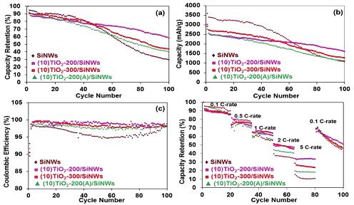
104 82
) as nanowires become amorphous after 1 full lithiation/delithiation cycle.")
105 the long-term trend. The reasons for this can be deduced from Figure 3.9. The single-crystal diffraction pattern of Si is no longer found in the SAD pattern of the TiO 2-200/SiNWs composite (Figure 3.9(a)) as nanowires become amorphous after 1 full lithiation/delithiation cycle. 22 A ring pattern corresponding to cubic LiTiO 2 is observed, despite the fact that the electrode is in the delithiated state. The calculated d-spacings are 0.204, nm, similar to what was previously found for cubic lithium titanate (LiTiO 2 ). 56 The HRTEM image in Figure 3.9(b) confirms the presence of crystalline LiTiO 2 phase embedded in an amorphous phase. The lattice fringe spacing is nm, corresponding to the (200) planes of cubic LiTiO 2. Also for (10)TiO 2-300/SiNWs, the LiTiO 2 phase is found with identical lattice spacings as for (10)TiO 2-200/SiNWs (see Figure 3.10). Figure 3.9: (a) Bright-field TEM and SAD pattern of TiO 2-200/SiNWs, (b) HRTEM and FFT pattern of the same showing 200LiTiO 2 lattice spacing. (c) Ti XPS spectrum after 1 cycle of TiO 2-200/SiNWs, TiO 2-300/SiNWs and TiO 2-200(A)/SiNWs and (d) bright-field TEM and SAD pattern of TiO 2-200(A)/SiNWs. In the Ti2p XPS spectrum for TiO 2-200/SiNWs in Figure 3.9(c), the peaks for TiO 2 are still visible, but have shifted to lower binding energies by ~0.75 ev. This shift reflects the change of Ti +4 to Ti +3 oxidation state upon formation of LiTiO The electrodes are in the delithiated state so the presence of LiTiO 2 indicates irreversible trapping of Li within the voltage 83

106 range used, leading to a lower coulombic efficiency in the first cycle. Note that TiO 2-200/SiNWs is the only composite for which a signal from the original interface with the electrolyte is still detected, showing that despite the lowest first cycle efficiency, this composite forms the thinnest SEI layer, although individual nanowires are still easily distinguishable in SEM micrographs after 1 cycle for all four electrodes (see Figure 3.11). Figure 3.10: TEM micrographs of (a)-(c) (10)TiO 2-200/SiNWs, (c)-(f) (10)TiO 2-300/SiNWs, (g) and (h) (10)TiO 2-200(A)/SiNWs after 1 cycle (after delithiation to 2 V). (a), (d) and (g) bright field micrographs with corresponding selected area diffraction (SAD) insert. (b), (e) dark field micrographs using a portion of 200 LiTiO2 ring pattern, highlighting coarser grain size of LiTiO 2 in (d). (f) dark field micrograph of the TiO 2 obtained using g=101 TiO2. HRTEM images of (c) (10)TiO 2-200/SiNWs, and (f) (10)TiO 2-300/SiNWs, highlighting partial crystallization of LiTiO 2 phase embedded in the amorphous region. The SAD pattern of lithiated TiO 2-200(A)/SiNWs (35 th cycle) does show evidence for LiTiO 2 (see Figure 3.12), but the amount is very small, consistent with the finding that anatase TiO 2 only transforms into LiTiO 2 in extremely small particles. 41 This is consistent with our CC 84

107 (Figure 3.7) and CV measurements (see Figure 3.13) on the planar TiO 2 films and previous findings on amorphous vs. crystalline TiO 55 2 which show higher total and irreversible capacity for the amorphous material. The CC curve for the planar anatase film shows a small plateau both on lithiation, at 1.7 V, and delithiation, 1.9 V, which is consistent with the fact that the SAD pattern of TiO 2-200(A)/SiNWs in Figure 3.9(d) shows only anatase TiO 2 and shows no evidence of residual, trapped Li. Figure 3.11: SEM images of (a) (10)TiO 2-200/SiNWs, (b) (10)TiO 2-300/SiNWs and (c) (10)TiO 2-200(A)/SiNWs after the first cycle at 0.1 C-rate. The above findings also explain the improved rate capability of TiO 2-200/SiNWs compared to bare SiNWs and anatase-coated SiNWs as LiTiO 2 provides an electrically conductive pathway 42 and the amorphous fraction has favourable Li transport properties. Even when delithiation is continued up to 3 V vs. Li/Li +, LiTiO 2 does not fully delithiate as Figure 3.12 shows. The (111) and (222) diffraction spots are also visible in the SAD pattern and definitively confirm that the structure is cubic. Dark-field images in Figure 3.10, taken using a portion the 200 LiTiO 2 diffraction ring, show a larger grain size of the LiTiO 2 phase for TiO 2-85

108 300/SiNWs, likely due to the higher residual precursor content at 200 C. Higher deposition temperatures are also reported to lead to slightly more dense coatings, irrespective of precursor residues, 51 which may also contribute to the difference in LiTiO 2 grain size. Measurements of the refractive index on the planar films also confirm this (see Figure 3.14). Figure 3.12: a) bright-field image of (10)TiO 2-200/SiNWs after 1 cycle between 0.01 and 3V vs. Li/Li + (b) corresponding SAD pattern confirming the cubic structure. (c)-(e) TEM micrographs of TiO 2-200(A)/SiNWs after 35 cycles (after lithiation to 0.01 V). (c) Bright field micrograph, (d) corresponding indexed selected area diffraction (SAD) pattern, (c) dark field micrograph using g=101 LixTiO2, (e) dark field micrograph obtained using g=200 LiTiO2. Figure 3.15 presents a cross-sectional view of TiO 2-200/SiNWs and TiO 2-200(A)/SiNWs after 100 cycles obtained using a focussed ion beam, together with EDX elemental mappings of silicon, titanium, carbon, oxygen and fluorine. The Ti and Si signals are strongly correlated for both composites and increase towards the substrate, showing that the TiO 2 coating completely covers the SiNWs, once more highlighting the ability of ALD to conformally coat the nanowires. For TiO 2-200/SiNWs, contrary to TiO 2-200(A)/SiNWs numerous voids and some individual nanowires are visible in the top part of the cross-section, indicating less SEI formation and increased mechanical support and reinforcement by the TiO 2 coating, consistent 86
109 87
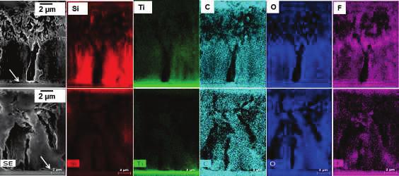
110 88
 SiNWs, (b) TiO 2-200/SiNWs, (c) TiO 2-300/SiNWs (d) TiO 2-200(A)/SiNWs after 100 cycles at 0.1 C. Figure 3.")
. (a), (c) and (e) are bright field micrographs with corresponding SAD inserts.")
111 coating indeed helps maintain the mechanical integrity of the nanowires during cycling. Figure 3.16: SEM images of (a) SiNWs, (b) TiO 2-200/SiNWs, (c) TiO 2-300/SiNWs (d) TiO 2-200(A)/SiNWs after 100 cycles at 0.1 C. Figure 3.17: TEM micrographs of, (a) and (b),tio 2-200/SiNWs, (c) and (d), TiO 2-300/SiNWs and (e) and (f), TiO 2-200(A)/SiNWs after 100 cycles (after delithiation to 2 V). (a), (c) and (e) are bright field micrographs with corresponding SAD inserts. (b), and (d) dark field micrographs using a portion of the 200 LiTiO2 ring, (f) dark field micrograph using g=101 TiO2. 89

112 The picture is similar for the 5 and 15 nm coatings as Figs and 3.19 show. The degree of agglomeration observed in Figure 3.16 increases in the same order as the CE, electrochemical cycling stability and rate capability decrease. Consistent with the electrochemical measurements in Figs. 3.6 and 3.8, there is a very big difference between TiO 2-200/SiNWs and TiO 2-200(A)/SiNWs in Figure From the TEM images taken after 100 cycles at 0.1 C-rate in Figure 3.17, a possible explanation for this can be found. The SAD pattern and dark field image (Figure 3.17(b)), which was obtained using a portion of the 200 LiTiO 2 diffraction ring, confirms the presence of LiTiO 2 also after 100 cycles. The LiTiO 2 phase looks to be homogeneously distributed over the entire width and length of the nanowire and has a very small grain size. A very different microstructure is found for TiO 2-200(A)/SiNWs where the anatase TiO 2 shell has cracked open and partially peeled off from the nanowire core. The dark-field image obtained from the 101 diffraction spot of anatase TiO 2, shows that each of the shell fragments is likely a single crystal. Because nanocrystalline materials can withstand higher deformation before fracturing, one would expect the anatase coating to be more vulnerable to fracture and delamination during cycling as the volume expansion of Si upon lithiation is very large. It can therefore be concluded that the two-phase nanostructure that has formed after the first cycle consisting of LiTiO 2 and amorphous TiO 2 is essential for obtaining good cycling stability. A similar argument applies for the difference between TiO 2-200/SiNWs and TiO 2-300/SiNWs that is evident in Figure 3.16(b) and 3.16(c). The LiTiO 2 grain size is clearly larger for the coating deposited at 300 o C (compare Figure 3.17(b)and 3.17(d)), although the difference is small compared to the annealed coating. That there is such a big difference in performance probably means the thermal stress in the as-made materials is also important. Figure 3.18: SEM images of (a) (5)TiO 2-200/SiNWs, (b) (15)TiO 2-200/SiNWs at 0.1 C-rate after 100 cycles. 90
, and (d) dark field micrographs obtained using a portion of the 200 LiTiO2 ring pattern. Figure 3.")
113 Figure 3.19: TEM micrographs of (a) and (b) (5)TiO 2-200/SiNWs, (c) and (d) (15)TiO 2-200/SiNWs after 100 cycles. (a) and (c) are bright field micrographs with corresponding SAD insert. (b), and (d) dark field micrographs obtained using a portion of the 200 LiTiO2 ring pattern. Figure 3.20 shows HAADF images and EELS elemental maps of bare SiNWs and the TiO 2 coated composites after 100 cycles. In this way, the spatial distribution of the SEI components across the nanowires can be visualized on the nanometre scale. Figure 3.20(a) shows that after 100 cycles, the bare SiNWs are completely covered by Li 2 CO 3 or Li alkylcarbonate as there is nearly perfect overlap between the Li, C and O signals around a Si core. The Li, C and O signals are strong over the entire imaged area, indicating the Li 2 CO 3 deposit is thick and that large amounts of SEI form on bare Si surfaces. For TiO 2-200/SiNWs (Figure 3.20(b)), there is a clear overlap between the Li and Ti-rich regions, indicating that also after 100 cycles, the LiTiO 2 phase is present as was also seen in TEM. Si is still concentrated in the core, in accordance with the SEM micrograph in Figure 3.16(b). At the outer surface of the structure depicted in Figure 3.20(b), there is a thin layer that is rich in Li and C, but this SEI layer is much thinner compared to bare SiNWs. For TiO 2-300/SiNWs and TiO 2-200(A)/SiNWs, the core region in the image is strongly depleted of Si and strong Si signal is found outside of the TiO 2 coating, indicating that the nanowire has broken up into several thinner strands as was already observed in Figure 3.17(c) and is also similar to what was observed for very thin Al coatings
 SiNWs, (b) TiO 2-200/SiNWs, (c) TiO 2-300/SiNWs and (d) TiO 2-200(A)/SiNWs after 100 cycles in the delithiated state.")
114 Figure 3.20: HAADF images and EELS elemental maps of Si, Ti, O, Li and C of cycled (a) SiNWs, (b) TiO 2-200/SiNWs, (c) TiO 2-300/SiNWs and (d) TiO 2-200(A)/SiNWs after 100 cycles in the delithiated state. This observation can be explained by considering the effects of the forces exerted by the coating on the underlying Si. The parts of the nanowire that still have the TiO 2 coating attached will be under compressive stress after lithiation due to the large difference in volume expansion between the Si and TiO 2. From the rate capability data in Figure 3.8(d), it is clear that the coating improves the charge transfer kinetics which means the coated regions of the nanowire contract faster during delithiation than regions where the coating has delaminated. This would cause the uncoated Si(Li) to be extruded through the gaps in the coating, leading to the microstructure consisting of thin strands of Si, parts of which are no longer enveloped by the coating, as is observed in Figure 3.20(c) and 3.20(d). It would then also be expected that higher charge and discharge rates exacerbate these effects and disintegration is indeed found to be much more severe, even for TiO 2-200/SiNWs, when cycling is performed continuously at higher rates (see Figure ). A material with a smaller grain size can sustain higher stress and deformation as a result of the larger volume expansion of SiNWs without delaminating and the observed trend in the mechanical stability of the coatings conforms to this. TiO 2-200/SiNWs developed the more fine- 92
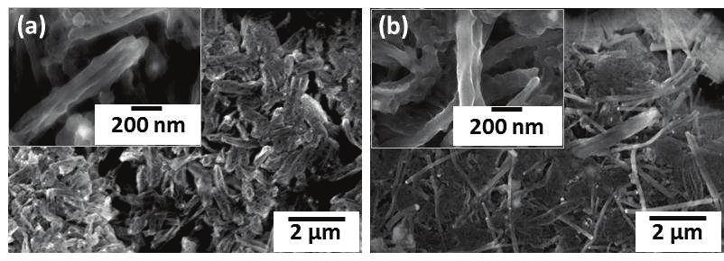
115 93
, and (c) bright field micrographs with corresponding SAD pattern insert. (b), and (d) dark field micrographs obtained using a portion of 200 LiTiO2 ring pattern. Figure 3.")
. (a), (c) and (e) bright field micrographs with corresponding SAD insert.")
116 Figure 3.23: TEM micrographs of (10)TiO 2-200/SiNWs at (a) and (b) 0.2 C-rate, (c) and (d) 0.5 C-rate after 100 cycles. (a), and (c) bright field micrographs with corresponding SAD pattern insert. (b), and (d) dark field micrographs obtained using a portion of 200 LiTiO2 ring pattern. Figure 3.24: (a) TEM micrographs of (a) and (b) bare SiNWs, (c) and (d) (10)TiO 2-200/SiNWs and (e) and (f) (10)TiO 2-200(A)/SiNWs after 100 cycles at different rates according to Figure 3d (after delithiation to 2 V). (a), (c) and (e) bright field micrographs with corresponding SAD insert. (b), dark field micrograph using a portion of diffuse ring, (d) dark field micrographs using a portion of 200 LiTiO2 ring pattern, and (f) dark field micrographs using g=101 TiO2. 94
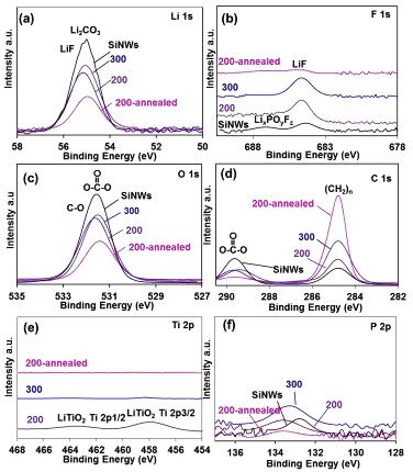
117 95
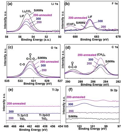
118 96
119 covered by electrolyte reduction products formed on freshly exposed Si during lithiation. This is further evidence of the passivating effect of TiO 2 coating, especially for TiO 2-200/SiNWs. The fact that trace amounts of Si are detected for TiO 2-300/SiNWs and TiO 2-200(A)/SiNWs is consistent with the extrusion mechanism described based on the EELS results. Table 3.2: Surface composition, in atomic percentages, as derived from the XPS spectra in Fig Figure 3.24 and Figure 3.25 for 1 and 100 times cycled electrodes Electrode SiNWs TiO 2-200/SiNWs TiO 2-300/SiNWs TiO 2-200(A)/SiNWs State Cycle 1 Cycle 100 Cycle 1 Cycle 100 Cycle 1 Cycle 100 Cycle 1 Cycle 100 C1s O1s Li1s F1s <1 < <1 3 Other (Si, Ti, P) < It should be noted here that as a way to improve coulombic efficiency and cycling stability, additions to, and wholesale reformulations of, the electrolyte have been studied as well. SiNWs cycled in dioxolane, which has a lower viscosity and a much higher resistance to reduction compared to carbonates, retain >2000 mah/g after 100 cycles and 1250 mah/g after 1000 cycles at 6 C. 58 However, ethers were abandoned early on in the development process of Li-ion batteries because of their poor oxidation resistance which makes them incompatible with conventional cathode materials. 59 Coatings have the distinct advantage that they are confined to one electrode only and therefore have no such compatibility issues. A graphical representation of the microstructural evolution of bare and TiO 2 coated SiNWs is shown in Figure Shown from left to right are an as-grown bare SiNW, a bare SiNW after 100 cycles including a thick SEI layer, an as-grown TiO 2 -coated SiNW and finally a TiO 2 -coated SiNW after 100 cycles. The picture illustrates how bare SiNWs disintegrate into thinner strands covered by thick SEI deposits as was shown in the inset of Figure 3.16(a) and previous in-situ microscopy studies. 32 For TiO 2-200/SiNWs, the coating adheres sufficiently strongly to the nanowire that the disintegration process that occurs for bare SiNWs is prevented 97
120 98
121 same way as we demonstrated here. PTFE and a conductive carbon additive are stable at our optimum ALD deposition temperature and direct deposition onto a powder electrode has also been shown to improve cycling stability to comparable levels as commercial graphite electrodes in a binder-free configuration. 63 For Si anodes, hollow nanospheres have already been shown to hold great promise as a binder-free system as well, 64 and ALD TiO 2 can be expected to help reduce the <10% capacity decay per 100 cycles even further. Thus, we have shown that ALDdeposited TiO 2 coatings greatly expand the number of ways in which the problematic cycling stability of Si can be improved. This is expected to become very important as Si anodes have been identified as the anode of choice for 3 rd generation automotive batteries by the US Department of Energy Conclusions Coating with TiO 2 not only improves the relative capacity retention by a factor two at 0.1 C and over a factor three at 5 C, but also increases the coulombic efficiency to 99%, compared to 95% for bare SiNWs, which is the highest value ever reported for SiNW-based electrodes in standard, carbonate-based electrolytes. Consistent with higher coulombic efficiency, SEM and XPS analysis showed less SEI formation overall and lower Li content compared to bare SiNWs for (10)TiO 2-200/SiNWs and (10)TiO 2-300/SiNWs, whereas crystallization of the TiO 2 into anatase by annealing is detrimental to the performance. EELS showed strongly reduced carbon signal in regions with intact TiO 2 coating, further confirming the passivating effect of TiO 2 towards SEI formation. The best performance was found for electrodes where the TiO 2 coating is initially fully amorphous. The amorphous coatings develop a highly dispersed microstructure of crystalline LiTiO 2 and an amorphous phase during cycling that is highly resistant to delamination. Though LiTiO 2 was shown to also form from anatase, (10)TiO 2-200(A)/SiNWs does not develop the same fine-grained microstructure and as a consequence has inferior capacity retention. The most important aspect of the coating seems to be that coverage should initially be 100%, all the way down to the nanowire base, as this was shown to be important in avoiding nanowire agglomeration followed by delamination from the conductive substrate. Future efforts can therefore be expected to concentrate on ALD and wet-chemical methods that are capable of producing conformal coatings on highly irregularly shaped substrates 99
122 3.5 Notes and references a University of Alberta, Chemical&Materials Engineering, th Street, T6G 2V4, Edmonton AB, Canada, Tel: ; pkalisvaart@gmail.com b National Institute of Nanotechnology, Saskatchewan Drive, T6G 2M9, Address, Address, Town, Country.; Tel: ; dmitlin@ualberta.ca Electronic Supplementary Information (ESI) available: [details of any supplementary information available should be included here]. See DOI: /b000000x/ 1. J. M. Tarascon, and M. Armand, Nature, 2001, 414, M. Armand, J. M. Tarascon, Nature, 2008, 451, S. Bijani, M. Gabas, G. Subias, J. Garcia, L. Sanchez, J. Morales, L. Martinez and J. R. Ramos-Barrado, J. Mater. Chem., 2011, 21, D. Deng, M. G. Kim, J. Yang Lee and J. Cho, Energy Environ. Sci., 2009, 2, M. Pfanzelt, P. Kubiak, S. Jacke, L. Dimesso, W. Jaegermann and M.Wohlfahrt-Mehrens, J. Electrochem. Soc., 2012, 159 (6), A809-A B. J. Landi, M. J. Ganter, C. D. Cress, R. A. DiLeo, and R. P. Raffaelle, Energy Environ. Sci., 2009, 7, H. Wu, G. Chan, J. W. Choi, I. Ryu, Y. Yao, M. T.McDowell, S. W. Lee, A. Jackson, Y. Yang, L. Hu, and Y. Cui, Nature Nanotechnology, 7, 2012, M. M. Thackeray, C. Wolverton, and E. D. Isaacs, Energy Environ. Sci., 2012, 5, W. H. Ryu, D. H. Nam, Y. S. Ko, R. H. Kim, H. S. Kwon, Electrochemica Acta, 2012, 61, F. F. Cao, Y. G. Guo, and Li-Jun Wan, Energy Environ. Sci., 2011, 4, X. Meng, X. Q. Yang and X. Sun, Adv. Mater., 2012, 24(27), T. Song, D. H. Lee, M. S. Kwon, J. M. Choi, H. Han, S. G. Doo, H. Chang, W. Park, W. Sigmund, H. Kim and U. Paik, J. Mater. Chem., 2011, 21, T.D. Hatchard and J.R. Dahn, J. Electrochem. Soc., 2004, 151, A V.L. Chevrier and J.R. Dahn, J. Electrochem. Soc., 2010, 157, A L.Y. Beaulieu, T.D. Hatchard, A. Bonakdarpour, M.D. Fleischauer and J.R. Dahn, J. Electrochem. Soc., 2003, 150, A J.L. Gómez-Cámer, J. Morales and L. Sánchez, J. Mater. Chem., 2011, 21,
123 17. T. Zhang, J. Gao, L. J. Fu, L. C. Yang, Y. P. Wu and H. Q. Wu, J. Mater. Chem., 2007, 17, C. Yu, X. Li, T. Ma, J. Rong, R. Zhang, J. Shaffer,Y. An, Q. Liu, B. Wei and H. Jiang, Adv. Energy Mater. 2012, 2, D. Larcher, S. Beattie, M. Morcrette, K. Edstroem, J. C. Jumas and J. M. Tarascon, J. Mater. Chem., 2007, 17, A. Gohier, B. Laïk, J. P. Pereira-Ramos, C. S. Cojocaru, P. Tran-Van, J. Power Sources, 2012, 203, K. Peng, J. Jie, W. Zhang and S. T. Lee, Appl. Phys. Lett., 2008, 93, E. L. Memarzadeh, W. P. Kalisvaart, A. Kohandehghan, B. Zahiri, C. M. B. Holt and D. Mitlin, J. Mater. Chem., 2012, 22, N. S. Choi, Y. Yao, Y. Cui and J. Cho, J. Mater. Chem., 2011, 21, T. Song, J. L. Xia, J. H. Lee, D. H. Lee, M. S. Kwon, J. M. Choi, J. Wu, S. K. Doo, H. Chang, W. Il Park, D. S. Zang, H. Kim, Y. G. Huang, K. C. Hwang, J. A. Rogers and U. Paik, Nano Lett., 2010, 10, R. Huang, X. Fan, W. Shen and J. Zhu, Appl. Phys. Lett., 2009, 95, T. Song, D. H. Lee, M. S. Kwon, J. M. Choi, H. Han, S. G. Doo, H. Chang, W. Park, W. Sigmund, H. Hansu Kim and U. Paik, J. Mater. Chem., 2011, 21, B. Laїk, D. Ung, A. Caillard, C. S. Cojocaru, D. Pribat and J. P. Pereira-Ramos, J. Solid State Electrochem., 2010, 14, K. Xu and A. Cresce, J. Mater. Chem., 2011, 21, D. Liu, and G. Cao, Energy Environ. Sci., 2010, 3, H. Chen, Z. Dong, Y. Fu and Y. Yang, J. Solid State Electrochem., 2010, 14, H. Chen, Y. Xiao, L. Wang and Y. Yang, J. Power Sources, 2011, 196, L. Q. Zhang, X. H. Liu, Y. Liu, S. Huang, T. Zhu, L. Gui, S. X. Mao, Z. Z. Ye, C. M. Wang, J. P. Sullivan and J. Y. Huang, ACS Nano, 2011, 5, A. Kohandehghan, W.P. Kalisvaart, M. Kupsta, B. Zahiri, B. Shalchi Amirkhiz, Z. Li, E.L. Memarzadeh, L.A. Bendersky, D. Mitlin, J. Mater. Chem. A, 2013, 1, H. C. M. Knoops, M. E. Donders, M. C. M. van de Sanden, P. H. L. Notten, and W. M. M. Kessels, J. Vac. Sci. Technol. A, 2012, 30(1),
124 35. S. K. Cheah, E. Perre, M. Rooth, M. Fondell, A. Hårsta, L. Nyholm, M. Boman, T. Gustafsson, J. Lu, P. Simon and K. Edström, Nano Lett., 2009, 9(9), X. Su, Q. Wu, X. Zhan, J. Wu, S. Wei, Z. Guo, J. Mater. Sci., 2012, 47, Z. Hong, M. Wei, T. Lan, L. Jiang and G. Cao, Energy Environ. Sci., 2012, 5, Y. Wang, X. Su and S. Lu, J. Mater. Chem., 2012, 22, H. W. Shim, D. K. Lee, I. S. Cho, K. S. Hong and D. W. Kim, Nanotechnology, 2010, 21, J. Wang, Y. Zhou, Y. Hu, R. O Hayre and Z. Shao, J. Phys. Chem. C, 2011, 115, M. Wagemaker, W.J.H. Borghols, F.M. Mulder, J. Am. Chem. Soc., 2007, 129, W.J.H. Borghols, D. Lützenkirchen-Hecht, U. Haake, E.R.H. van Eck, F.M. Mulder, M. Wagemaker, Phys. Chem. Chem. Phys., 2009, 11, Z. Y. Zeng, J. P. Tu, X. H. Huang, X. L. Wang, X. B. Zhao and K. F. Li, Electrochem. Solid-State Lett., 2008, 11(6), A105-A M. Pfanzelt, P. Kubiak, M. Fleischhammer, M. Wohlfahrt-Mehrens, J. Power Sources, 2011, 196, R.F. Egerton, Electron energy-loss spectroscopy in the electron microscope. 3rd ed2011, New York: Springer. 46. R. Methaapanon, R.F. Bent, J. Phys. Chem. C, 2010, 114, NIST XPS database at L. Brewer, Chemical Reviews, 1953, 52, Y. Okada, Y. Tokumaru, J. Apl. Phys., 1984, 56, T. Hanada, N. Soga, M. Ohkawa, J. Non-Cryst. Solids, 1986, 88, Y. Huang, G. Pandraud, P.M. Sarro, J. Vac. Sci. Technol. A, 2013, 31, 01A V. L. Chevrier, J. W. Zwanziger and J. R. Dahn, Can. J. Phys., 2009, 87, X.H. Liu, J.W. Wang, S. Huang, F. Fan, X. Huang, Y. Liu, S. Krylyuk, J. Yoo, S.A. Dayeh, A.V. Davydov, S.X. Mao, S.T. Picraux, S. Zhang, J. Li, T. Zhu, J.Y. Huang, Nature Nanotech., 2012, 7, L. Baggetto, R. A. H. Niessen, F. Roozeboom and P. H. L. Notten, Adv. Funct. Mater., 2008, 18,
125 55. H. T. Fang, M. Liu, D. W. Wang, T. Sun, D. S. Guan, F. Li, J. Zhou, T. K. Sham and H. M. Cheng, Nanotechnology, 2009, 20, D. Wang, D. Choi, Z. Yang, V. V. Viswanathan, Z. Nie, C. Wang, Y. Song, J. G. Zhang and J. Liu, Chem. Mater., 2008, 20, M. S. Wu, M. J. Wang, J. J. Jow, W. D. Yang, C. Y. Hsieh, H. M. Tsai, J. Power Sources, 2008, 185, G. V. Etacheri, U. Geiger, Y. Gofer, G. A. Roberts, I. C. Stefan, R. Fasching and D. Aurbach, Langmuir, 2012, 28, K. Xu, Chemical Reviews, 2004, 104, D. Aurbach, J. Power Sources, 2000, 89, Y. Yao, N. Liu, M.t. McDowell, M. Pasta, Y. Cui, Energy Environ. Sci., 2012, 5, Z. Li, L. Zhang, B. Shalchi-Amirkhiz, X. Tan, H. Wang, B. C. Olsen, C. M. B. Holt, D. Mitlin, Adv. Energy Mater., 2012, 2, Y. S. Jung, A. S. Cavanagh, L. A. Riley, S-H. Kang, A. C. Dillon, M. D. Groner, S. M. George, S-H. Lee, Adv. Mater., 2010, 22, Y. Yao, M. T. McDowell, I. Ryu, H. Wu, :L. Hu, W. D. Nix, Y. Cui, Nano Lett., 2011, 11, US Department of Energy Vehicle Technologies Program eere.energy.gov. 103
126 4 Si Nanotubes ALD Coated with TiO 2, TiN or Al 2 O 3 as High Performance Lithium Ion Battery Anodes Material in this chapter has been published in: E. Memarzadeh Lotfabad, P.Kalisvaart, A. Kohandehghan, Kai Cui, Martin Kupsta, Behdokht Farbod, David Mitlin, J. Mater. Chem. A, 2014, 2, Introduction The specific energy storage capacity and the charge/discharge rate of lithium ion batteries are critical for their use in electric vehicles (EVs). 1,2 Increasing specific energy capacity remains a challenge despite the significant gains in rate capability and safety through the use of new materials. Replacing graphitic carbon with Si as the anode material can considerably increase the energy storage capacity of the battery. However commercialization remains limited by several factors, including the materials' accelerated failure relative to graphite. Mechanical failure is associated with the dramatic volume change during lithiation, which causes major stresses, fracture and contact loss of the active material, Si, with the current collector 3,4. Consequently, relatively rapid capacity loss will occur. Studies show that mechanical failure can be mitigated by using Si-based nanostructures including solid nanoparticles, 5 thin films, 6,7 or hollow shapes such as nanotubes, hollow nanoparticles and related nanostructures. 3,8-15 These studies indicate that a key feature for electrode design is not only to provide sufficient free space during lithiation and to keep the dimensions of the structures well within the nano-scale regime, but also to tailor materials' active surface to remain primarily compressively stressed during lithiation. One outstanding example of such a strategy is to have hollow Si nanostructures where only the inner surface is active towards Li while the outer surface is passivated by a thick layer of native oxide. 11 In a hollow core-shell nanostructures, the confining oxide layer forces the core to expand inwards into the hollow space. The outer electrode interface with the electrolyte is mechanically constrained and remains static during both lithiation and delithiation. This 104
127 makes the material cycle over 6,000 times in half cells while retaining more than 85% of their initial capacity at C/5. Silicon nanotubes (SiNTs) is one attractive electrode configuration that improves electrochemical performance. 11,12,14 The axial void space within the nanotubes provides additional free space to accommodate the 300% volume expansion associated with lithiating Si to Li 15 Si 4. Such electrodes exhibit initial coulombic efficiencies typically in the 85% range, and capacity retentions of near 80% for up to 50 cycles. 12,14,16 Typical cycling coulombic efficiencies are in the % range, 14,16 which means that a full cell lithium ion battery with initially balanced anode/cathode capacity would last somewhere between 20 and 33 cycles before running out of Li ions. Moreover these cycling lifetimes would be even lower due to lower coulombic efficiency during the initial cycles. It would therefore be highly desirable to improve both the initial coulombic efficiency and the cycling columbic efficiency of such hollow nanostructures. Poor coulombic efficiency is typically associated with the irreversible and continuous formation of a solid electrolyte interface (SEI). Both the solvent and salt of the electrolyte solution are thermodynamically unstable and undergo reduction on the anode, which operates at low potentials close to metallic lithium. 17,18 A material with a large surface-to-volume ratio will therefore cause higher irreversible capacity losses. 19,20 These surface films passivate the anode surface and prevent further decomposition of the electrolyte solution. However, high volume changes experienced by silicon during electrochemical cycling can continuously weaken and fracture the SEI layer, exposing fresh silicon to the electrolyte with each cycle. This will form a new SEI layer mostly composed of electrolyte reduction products such as Li 2 CO 3 and increase the amount of SEI with each cycle. The instability of the SEI can eventually lead to overall capacity loss and failure of the battery Besides solvent reduction products such as Li 2 CO 3 and alkyl carbonates, SEI also partially consists of LiF which is a (electroless) decomposition product of the LiPF 6 salt but can also be formed through reaction with trace amounts of water to HF and eventually LiF. 25,26 Thin surface coatings have been shown to be effective for stabilizing the SEI layer, and hence improving the coulombic efficiency in Si. The use of functional coatings such as carbon, conductive polymer, 30 Cu, 31 Ag, 32 Al, 33 Mg and Mg 2 Si, 34 Al 2 O 26, , TiO 2, 21,37-40 SnO 2, 41,42 and TiN 43 on the surface of silicon and of other anodes have shown promising outcomes. 105
128 Coatings can act as a buffer layer between the active electrode and electrolyte, and prevent the formation of excessive amounts of SEI. This approach has been explored in some detail for anode materials with solid (only an outer Li active surface) geometries such as solid nanowires, nanoparticles, nanorods, etc. However hollow (an outer and an inner Li active surface) nanostructures have been explored far less. The key difference between these two architectures is that in materials such as Si nanotubes there are potentially two, rather than one, surfaces where SEI may form from the get-go. In this study we employ atomic layer deposition (ALD) to coat TiO 2, Al 2 O 3 and TiN onto hollow Si nanotubes to demonstrate that it is not entirely correct to assume that passivating only the outer surface is enough to achieve optimum coulombic efficiency. Rather, we show that an additional improvement may be obtained by coating the inner surface as well. For example we achieve an average coulombic efficiency of 99.9% (among the highest ever reported for any hollow Si nanostructure) for Si nanotubes coated with TiO 2 both their inside and their outside, versus 99.1% with an outer coating only. While this difference seems small, with all else being equal in a real device it may mean a lifetime of 1000 cycles rather than 111 cycles. Since electrochemical reduction - based growth of SEI occurs preferentially on exposed fresh Si, rather than on pre-existing SEI, 21,44,45 a broader implication of our findings is that some material degradation occurs on the inner surfaces as well. Thus, lithiation-induced expansion (and hence the stress state) on the inside of such hollow structures may be more complex than originally envisioned. 4.2 Experimental Synthesis of coated Si nanotubes Si nanotubes (SiNTs) were grown using ZnO nanorods as sacrificial templates, similarly to what was originally done in ref 14. A 200-nm-thick ZnO seed layer was first deposited onto 316L stainless steel spacers (diameter 15.4 mm) using magnetron sputtering (Orion 8, AJA international). We used Ar gas with a purity of grade 5N at a sputtering pressure of 5 x10⁻³ mbar, with a maximum base pressure of 5x10⁻⁸ mbar. ZnO nanorods (NRs) were then grown on the seed layer by incubating in an aqueous solution containing M zinc nitrate hexahydrate and M hexamethylenetetramine at 90 ºC for 24 hr. Then, samples were thoroughly rinsed with deionized water and dried at 90 C. ZnO nanorods were transferred to a CVD chamber for 106
129 deposition of the Si. Deposition of Si was achieved at 540 ºC for 15 min with the mixture of H 2 and SiH 4 at a pressure of 300 mtorr, producing nm thick Si shells. In the same CVD furnace, after Si deposition, the ZnO was selectively removed by annealing at 600 ºC for 24 hr with 50% H 2 in Ar, first reducing the ZnO and then evaporating the Zn. Atomic layer deposition (ALD) conformal coatings were applied before and/or after deposition of Si, so as to coat the inside of the SiNTs (ALD onto sacrificial ZnO, performed prior to Si deposition), the outside of the SiNTs (ALD after Si deposition), or both. The total thickness of the coatings was 3 nm, either as an individual 3 nm thick inner or outer layer, or as 1.5/1.5 nm inner and outer layer together. Since the inner and the outer nanotube surfaces have different areas, the actual mass loading was not exactly identical for each of the three cases. Each electrode has approximately 0.2 mg Si active mass. A 3 nm TiO 2 coating on the outside adds mg to the sample mass. For 3 nm TiO 2 on the inside, this is mg and for double-sided coating mg. This is equivalent to ~ 0.11, 0.13, 0.12, 0.13 mg/cm 2 for bare SiNTs, TiO 2 on the outside, inside and double sides of the nanotubes, respectively. TiO 2 was deposited from titanium isopropoxides Ti(OCH(CH 3 ) 2 ) 4 as the titanium source and O 2 as the oxygen source. Argon was used as the carrier gas. The XPS spectra of the as-synthesized electrodes demonstrated that the relative intensity of the carbon signal was higher when TiO 2 was coated on the outside or both sides of the SiNTs compared to bare SiNTs and inner TiO 2 coating. The extra intensity over that of adventitious carbon comes from the residual organic groups in the ALD precursor that have not entirely volatilized. Trimethyl aluminium (TMA) and O 2 were employed as precursors for Al 2 O 3. TiCl 4 and N 2 were employed as precursors for TiN. All coatings were deposited at 200 o C. The film thickness was confirmed both by ex-situ rate measurements on planar supports and by TEM analysis of the nanotube architectures Electrochemical testing CR2032 button half-cells were assembled using the SiNTs as working electrodes and Li foil (15.4 mm diameter) as counter electrodes. Assembly was performed in an Ar-filled glove box with less than 0.1 ppm oxygen and moisture content. Lithium metal foil was separated from the working electrode with a polyethylene separator (MTI technologies, porosity of 36 44% and 0.03 µm pore size). The electrolyte was 1 M LiPF 6 dissolved in a 1:1:1 volume ratio of ethylene carbonate (EC): dimethyl carbonate (DMC): diethylcarbonate (DEC) organic solvents. 107
130 Galvanostatic discharge/charge cycling was carried out on a computer controlled BT2000 Arbin potentiostat in the voltage range of 0.01 to 2 V (vs. Li/Li + ). A constant current density was used for discharge/charge experiments at rates between 0.2 and 5C. Electrochemical impedance spectroscopy (EIS) of the half-cell electrodes was measured using a Princeton Applied Research VersaSTAT3 frequency response analyzer (FRA). An AC voltage of 10 mv amplitude was applied over a frequency range of 0.01 Hz to 1 MHz Microstructural Characterization For post-cycling characterization the coin cells were disassembled in the same glove box. Subsequently, the cycled electrodes were rinsed thoroughly with acetonitrile to remove excess electrolyte and kept in the glove box to dry overnight. The samples were characterized using field emission scanning electron microscopy (FE-SEM) (Hitachi S-4800) and transmission electron microscopy (TEM) (JEOL 2010, 200 kv). Electron energy loss spectroscopy (EELS) measurements were conducted using a JEOL 2200FS TEM operated at 200 kv in a scanning mode (STEM) with a nominal analytical beam size of 0.5 nm. High angle annular dark field (HAADF) images were recorded simultaneously with the EELS analysis. The software employed for signal collection and data extraction from EELS spectra was Digital Micrograph (Gatan, Inc.). The data extraction was performed by following the standard procedure of preedge background subtraction and integration on the edge 46. We mapped Silicon, Carbon, Titanium, and Oxygen by integrating over core-loss edges of Si-L, C-K, N-K, Ti-L, and O-Kedge, respectively. Lithium maps for cycled materials were obtained from Li-K edge at ev. Cross-sectional SEM images of the as-prepared and cycled samples were acquired using a Hitachi NB5000 dual-beam focused ion beam (FIB)/SEM. Surface composition of electrode materials is characterized via X-ray photoelectron spectroscopy (XPS) using an ULTRA (Kratos Analytical) spectrometer with Al K α X-ray source (hν= ev) run at 210 W. Data collection was conducted under ultrahigh vacuum (10-9 Torr) over an area of μm 2. All XPS spectra were calibrated from the universal hydrocarbon contamination using the C1s peak at ev. We used CasaXPS software was used to analyze XPS data. Background subtraction was done using a nonlinear Shirley-type model. 108
131 4.3 Results and Discussion As-synthesized microstructures We will employ a shorthand designation to label the various SiNTs samples that is based on the type and the location of the coating. As described in the experimental section, the three coatings TiO 2, Al 2 O 3 and TiN were deposited either on the inside (3 nm) outside (3 nm), or on both sides (1.5 nm inner, 1.5 nm outer) of the nanotubes. When only the inside of the nanotubes was coated, the designation is TiO 2 /SiNTs, Al 2 O 3 /SiNTs, TiN/SiNTs. When the outside is coated the designation is SiNTs/TiO 2, SiNTs/Al 2 O 3, SiNTs/TiN. When both sides are coated, the designation is TiO 2 /SiNTs/TiO 2, Al 2 O 3 /SiNTs/Al 2 O 3, TiN/SiNTs/TiN. Figure 4.1 shows representative top view SEM micrographs of the (a) SiNTs, (b) SiNTs/TiO 2, (c) SiNTs/Al 2 O 3 and (d) SiNTs/TiN electrodes. Typical diameters of the SiNTs were in the nm range. From cross section SEM and FIB (Figure 4.1(e)) we measured the nanotubes to be in the µm range in length, and to be grown almost vertically with respect to the substrate. Figure 4.2 presents TEM micrographs of the as-synthesized SiNTs electrodes, displaying bright field images and indexed selected area diffraction patterns for each material Figures 4.2(a) and 4.2(b) show the uncoated SiNTs. In all cases the SiNTs were polycrystalline, as highlighted in the dark field micrograph obtained using a portion of 111 Si ring pattern that shows the Si nanocrystallites within the tube walls. Such initial Si microstructure existed in all the samples, with no discernable sample-to-sample variation in the grain size. Figure 4.2(c-e) show bright field images and indexed SAD patterns of SiNTs/TiO 2, SiNTs/Al 2 O 3 and SiNTs/TiN, respectively. The TiO 2 and Al 2 O 3 coatings are amorphous while the TiN appears to be nanocrystalline and its most intense ring matches with the 200 reflection of the equilibrium cubic structure ( Fm3m ) of TiN. 109
 FIB cross-section of SiNTs/TiO 2 showing the height of the nanotubes as approximately 3 µm. Figure 4.2: TEM micrographs of the as synthesized materials.")

132 Figure 4.1: SEM micrographs of (a) SiNTs, (b) SiNTs/TiO 2, (c) SiNTs/Al 2 O 3, (d) SiNTs/TiN electrodes. (e) FIB cross-section of SiNTs/TiO 2 showing the height of the nanotubes as approximately 3 µm. Figure 4.2: TEM micrographs of the as synthesized materials. (a) and (b) uncoated SiNTs showing a bright field micrograph with the corresponding indexed SAD pattern, and a dark field micrograph of the polycrystalline Si obtained using a portion of 111 Si ring pattern. (c) Bright field micrograph and indexed SAD pattern of SiNTs/TiO 2, (d) SiNTs/Al 2 O 3, (e) SiNTs/TiN The TiO 2 and Al 2 O 3 coatings are amorphous whereas TiN is nanocrystalline. 110
133 For TiO 2 /SiNTs/TiO 2 and TiO 2 /SiNTs shown in Figure 4.3(a-b) and 4.3(c-d), the anatase 101 reflection is visible as the inner coating is already present during the high-temperature Si deposition and the reduction step of ZnO, causing it to crystallize. Figure 4.3: TEM micrograph of the as synthesized materials, showing a bright field micrograph with the corresponding indexed SAD pattern, and a dark field micrograph of the polycrystalline Si obtained using a portion of 111 Si ring pattern. (a) and (b) TiO 2 /SiNTs/TiO 2 ; (c) and (d) TiO 2 /SiNTs. Figure 4.4 shows HRTEM micrographs, highlighting the walls of the uncoated and the coated as-synthesized SiNTs. Figure 4.4(a) shows the uncoated specimens, highlighting the wall thickness on one SiNT that is 22 nm. Most of the nanotubes we examined had wall thicknesses in this range. The fast fourier transform (FFT) pattern insert shows a 111 ring of Si, in agreement with the SAD analysis of Figure 4.2. The magnified images in Figures 4.4(b) and 4.4(c), taken from regions 1 and 2, highlight the lattice fringes of the polycrystalline Si walls, and the amorphous ~ 2 nm thick silicon oxide present on the inner and outer wall surfaces. Since in this case the micrograph was obtained from the inner tube wall, HRTEM image actually shows the oxide overlapping with the crystalline Si. Figures 4.4(d-f) show the wall of SiNTs/TiO 2, demonstrating the highly uniform and defect-free amorphous TiO 2 coating on the 111
 of (a)-(c) uncoated SiNTs; (d)-(f) and (d) SiNTs/TiO 2 ; and (g) (i) TiO 2 /SiNTs/TiO 2.")
134 outer Si surface. The thickness of the TiO 2 is quite close to the nominal, i.e. 3 nm. For TiO 2 /SiNTs/TiO 2, the magnified images in Figure 4.4(i) highlights lattice fringes of Si and 1.5 nm amorphous outer TiO 2. Figure 4.4: HRTEM images including fast fourier transforms (FFTs) of (a)-(c) uncoated SiNTs; (d)-(f) and (d) SiNTs/TiO 2 ; and (g) (i) TiO 2 /SiNTs/TiO 2. High magnification images of areas marked by rectangles 1 and 2 highlight the lattice fringes for Si and the amorphous structure of the outer TiO 2 coating. Figure 4.5 shows the HAADF images and the EELS maps of (a) uncoated SiNTs, (b) SiNTs/TiO 2, and (c) TiO 2 /SiNTs/TiO 2. In Figure 4.5(d) the line scan profile along the nanotube diameter (red dashed line) shows the hollow core-shell structure for TiO 2 /SiNTs/TiO 2. As expected, no Zn signal was detected inside the tubes, as the metal is known to simultaneously evaporate during the reduction process. 14 The HAADF image and EELS maps of the uncoated SiNTs support the conclusion that Si is oxidized on the inner surface of the tubes as well as on the outer, as indicated by the arrows. The former occurs primarily due to the oxygen that is released during the decomposition of ZnO. The SiNTs/TiO 2 material shows an analogous relatively diffuse oxygen signal on the inner tube surface (there is no reason why it should differ), and a much sharper Ti and O signal on the outer tube walls. TiO 2 is thermodynamically 112
 shows a double spike in both the Ti and O signal at either end of the nanotube, confirming the presence of the 1.5 nm TiO 2 coating on both sides of the Si nanotube wall. Figure 4.")
135 more stable than SiO 21,47 2, and should at least partially reduce the native oxide upon its deposition. The line scan in Figure 4.5(d) shows a double spike in both the Ti and O signal at either end of the nanotube, confirming the presence of the 1.5 nm TiO 2 coating on both sides of the Si nanotube wall. Figure 4.5: HAADF images and EELS maps of (a) uncoated SiNTs, (b) SiNTs/TiO 2, and (c) TiO 2 /SiNTs/TiO 2. Native oxide layers on Si are indicated with arrows. (d) line scan profile along the nanotube diameter (red dashed line) shows the hollow core-shell structure for TiO 2 /SiNTs/TiO 2 where 2 spikes in both the Ti and O signals spaced ~20 nm apart are visible on either end of the scanned area. Figure 4.6 shows the XPS spectra for the as-synthesized materials. None of the samples showed any signal associated with the Zn 2p spectra. For uncoated SiNTs and TiO 2 /SiNTs, the XPS spectra show the Si n+ peak at 103 ev. This binding energy is consistent with Si in its highest oxidation state (i.e. Si 4+ ) indicative of stoichiometric SiO However, for SiNTs/TiO 2 and TiO 2 /SiNTs/TiO 2, the Si n+ peak shifts to a lower binding energy. This is indicative of lower Si oxidation states (Si 3+ and Si 2+ ), and consistent with ALD titanium at least partially reducing 113
 2 ) that have not volatalized.")
136 the SiO 2 surface. A peak shift can also be observed in O1s spectra, going from ev for uncoated SiNTs and TiO 2 /SiNTs, to ev for SiNTs/TiO 2 and TiO 2 /SiNTs/TiO 2. The relative intensity of the carbon signal is higher for SiNTs/TiO 2 and TiO 2 /SiNTs/TiO 2, originating from the residual organic groups in the ALD precursor (i.e. OCH(CH 3 ) 2 ) that have not volatalized. The SiNTs are sufficiently thick to block most of the XPS signal from the inner TiO 2 coatings of the TiO 2 /SiNTs specimen. Lithium alkoxides are normally one of the main constituents of the SEI layer. 17 The residual isopropoxide ligands should convert to LiOCH(CH 3 ) 2 during the first lithiation and should not impair electrode reversibility. Figure 4.6: XPS spectra of the TiO 2 -coated SiNTs electrodes in as-synthesized state Electrochemical performance and post-cycled microstructure When the composites are electrochemically cycled substantial differences emerge in their performance. Table 4.1 lists the 1 st discharge specific capacity, first-discharge capacity loss ([1 st discharge capacity 2 nd discharge capacity]/[1 st discharge capacity])x100%, and initial coulombic efficiency (CE), (1 st delithiation capacity/ 1 st lithiation capacity). The data is presented for electrodes tested at a rate of 0.2 C. Because the experimentally measured capacity of TiO 2 is more than an order of magnitude lower than that of Si ( vs mah/g), the coated SiNTs electrodes show a slightly lower initial specific capacity. The first discharge capacity loss is lower and the coulombic efficiency is higher for TiO 2 - SiNTs nanocomposites, the improvement being the most pronounced when the TiO 2 is present on both surfaces of the SiNTs. 114
137 Table 4.1: Galvanostatic cycling results for the uncoated and coated SiNW electrodes, tested at 0.2 Initial First discharge First discharge Coulombic Electrode specific capacity (mahg -1 capacity loss (%) efficiency ) (%) SiNTs SiNTs/TiO TiO 2 /SiNTs/TiO TiO 2 /SiNTs SiNTs/Al 2 O Al 2 O 3 /SiNTs/Al 2 O Al 2 O 3 /SiNTs SiNTs/TiN TiN/SiNTs/TiN TiN/SiNTs It is known that in the presence of oxygen the surface of Si naturally passivates to SiO 2 both at ambient and at higher temperatures, e.g. 49 The presence of SiO 2 contributes to the initial capacity loss since the conversion of SiO 2 into lithium oxides during the lithiation process is irreversible. 50,51 An irreversible conversion reaction of TiO 2 to Li 2 O and Ti has not been directly observed. 52 However during the first discharge there is irreversible trapping of Li that is known to occur for nm-scale amorphous TiO 2 films that partially transform to stable LiTiO 2 nanocrystallites. 21 At voltages roughly below 0.7 V vs. Li/Li +, the electrolyte reduction product SEI will still form on either surface. 21,53,54 However, since the highest initial CE (89% vs. 84% for uncoated) and lowest initial first-discharge capacity loss (12% vs. 17%) are achieved in TiO 2 /SiNTs/TiO 2 electrodes, one can argue that on the balance a TiO 2 - electrolyte interface is more advantageous than a SiO 2 - electrolyte interface. The overall trend for TiN and Al 2 O 3 is the same as with TiO 2 ; a slight reduction of the first discharge capacity, but an improvement in the first discharge capacity loss and in the initial CE and the highest initial CE is found for double-sided coated SiNTs. The Al 2 O 3 coating may 115
138 partially reduce the SiO 2 (depending on the chemical activity of the Al during the ALD process), and forms a Li-Al-O glass film in the lithiated state. It has also been shown to possess excellent lithium ion conductivity (up to Ω 1 cm 1 ) due to the partially occupied Li ion sites inside. The extent of SEI formation on Li-Al-O surfaces is known to be relatively low. 26 Bulk or thin film TiN does not store Li, though near-atomically thin TiN layers do permit lithium flux through the grain boundaries and other defects. 43 Interestingly, despite TiN not being expected to reduce the underlying SiO 2, it provides analogous positive improvement in both the CE and the first discharge capacity loss as does the TiO 2 and the Al 2 O 3. This implies that it is the extent of the initial SEI formation on a given oxide or nitride surface that is critical for improving both factors. Figure 4.7 shows the constant current (CC) voltage profiles and the differential capacity curves (dcapacity/dv) of the uncoated SiNTs and the coated specimens. The samples were tested at 0.2 C, and the data are shown for the 1 st, 2 nd, 20 th, 50 th and 100 th cycles. Figures 4.7(a) and 4.7(b) represent the uncoated SiNTs while Figures 4.7(c) and 4.7(d) show the data for TiO 2 /SiNTs/TiO 2. The same data for the rest of the specimens are shown in Figure For all electrodes, there is a low voltage plateau during the first discharge, which can be assigned to the lithiation of crystalline Si into an amorphous Li x Si phase with a progressively increasing Li content at lower voltages. This sloping plateau shows up as a peak in the differential capacity profile during cycle 1, centered at roughly at 0.12 V. During subsequent cycles the slope of this plateau begins to vary, leading to multiple peaks in the dc/dv plots. The multiple plateau slopes are attributed to amorphous Li y Si phases with differing composition, and hence differing local atomic arrangements and free energies. 55 It is known that lithiation of Si to below 50 mv vs. Li/Li + results in the formation of a crystalline Li 15 Si 4 phase. 56 This can be observed as a small peak in the differential capacity curves near this voltage. The anodic peak in the differential capacity during charging, centered at roughly 0.45 V, corresponds to the voltage plateau associated with the two-phase region where Li 15 Si 4 phase converts back to a-li y Si
139 117
140 118
141 119
 compare the capacity retention and CE versus cycle number for the samples with the coating on the outside of the nanotubes. The electrodes were tested at a rate of 0.2 C.")
142 anatase TiO 2 (see Figure 4.8(e) and 5.8(f)). Al 2 O 3 is amorphous, remains so upon lithiation 60 and does not produce a distinct response in either CC or dc/dv profiles. Figures 4.11(a-c) compare the capacity retention and CE versus cycle number for the samples with the coating on the outside of the nanotubes. The electrodes were tested at a rate of 0.2 C. By cycle 2 all the electrodes exhibit similar specific capacities that are in the mah/g range. The bare SiNTs and SiNTs/TiO 2 were tied for the lowest, while SiNTs/TiN and SiNTs/Al 2 O 3 were tied for the highest of these values. However by cycle 100 the differences were much more significant: The uncoated SiNTs possessed a capacity of 1665 mah/g, SiNTs/TiN was at 1774 mah/g, SiNTs/Al 2 O 3 was at 1921 mah/g, while SiNTs/TiO 2 was at 1936 mah/g. On the basis of the percentage of the initial capacity retention, the differences were just as significant: The bare SiNTs retained 54% of the initial capacity, TiN coated retained 59%, while Al 2 O 3 and TiO 2 coated nanotubes were both at 66%. Figure 4.11(c) demonstrates that the steady-state coulombic efficiency vs. cycle number data is consistently higher for all the coated electrodes. Taken at cycle # 50, the CE values are 97.5% for SiNTs, 99.3 % for SiNTs/TiN, 99.6% for SiNTs/TiO 2 and 99.8% for SiNTs/Al 2 O 3. Of course there is some scatter in the data; however the trend is consistent at other cycle numbers. Figure 4.11: (a) and (b) Capacity retention vs. cycle number for SiNT s coated with 3 nm of Al 2 O 3, TiN, and TiO 2 on their outer surface, tested at 0.2 C rate; (c) corresponding Coulombic efficiency; and (d) rate dependence of capacity retention as a percentage of capacity at 0.2 C. 120
143 The rate capability of the bare and outer-coated SiNTs was also tested and the results are shown in Figure 4.11(d). For TiO 2 coated SiNTs, the results of all three electrode configurations, inner, outer and double-sided, are included. The TiO 2 /SiNTs/TiO 2 electrode demonstrates by far the best rate capability, with a capacity retention of around 50% at 5C, versus 20% for the uncoated baseline. Of the three coatings, the best rate capability is achieved with TiO 2. It has been demonstrated that a high electronic conductivity and a high Li-diffusion coefficient are both key for improving the rate capability of an electrode. 61 TiN offers excellent electrical conductivity 43,62 and a Li-Al-O glass offers excellent Li-ion conduction. Our recent study on TiO 2 coated silicon nanowires demonstrated that during lithiation cycling, the structure of amorphous ALD TiO 2 evolves into a nanocomposite composed of a highly Li - active amorphous TiO 2 and a highly electrically conducting but Li inactive LiTiO Thus, uniquely both objectives are achieved with the TiO 2 coating: the LiTiO 2 providing an electrically conductive pathway 63 and the amorphous fraction enhancing Li transport at the electrodeelectrolyte interface. Therefore, we argue that it is the unique two-phase microstructure of lithiated TiO 2 that offers both high ionic and electrical conductivity that makes the rate capability of the outer-tio 2 -coated materials stand out as superior. The presence of the TiO 2 coating on both sides of the nanotube, versus just an outer or an inner coating, is also quite beneficial for further improving the rate capability. A straightforward argument may be made that this provides a larger electrical conduction pathway to the current collector and a higher surface area with fast Li transport. Figure 4.12 shows the XPS data for all the coatings and the uncoated baseline, after 100 cycles. For the Al 2 O 3 coating the Li 1s and O 1s spectra show a shift to higher binding energies confirming the formation of Li-Al-O film. 36 Li 2 CO 3 is a well-known electrolyte reduction product, 26 the irreversible formation of which is associated with poor coulombic efficiency. Comparison of XPS spectra of SiNTs with different coating materials (Figure 4.12(a-e)) demonstrate that they all minimize the amount of cycling-induced carbonate formation during cycling as compared to the uncoated electrodes. Of the three coatings, the highest relative amount of Li 2 CO 3 occurs in bare SiNTs followed by SiNTs/TiN and the lowest amount by far in SiNTs/Al 2 O 3, agreeing with the CE results in Figure 4.11(c). The fact that strong Al signal is still detected for SiNTs/Al 2 O 3 even after 100 cycles shows that the amount of SEI on the outer surface of the SiNTs is relatively low for this electrode. On the other hand, no Ti signal is 121
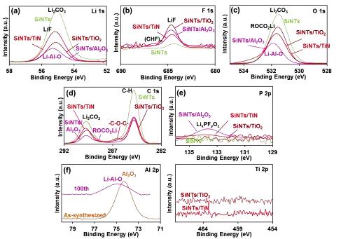
144 122
145 123
146 Figure 4.14: (a) and (b) Capacity retention vs. cycle number of Al 2 O 3 coated SiNTs, highlighting the role of coating location, i.e. inner surface, outer or both. (c) corresponding coulombic efficiency. Figure 4.15: (a) and (b) Capacity retention vs. cycle number of TiN coated SiNTs, highlighting the role of coating location, i.e. inner surface, outer or both. (c) corresponding coulombic efficiency. 124
147 125

148 The role of inner and/or outer coating layer and the influence on cycling performance can be explained by TEM and SEM analysis of the post cycled nanotubes. These results are shown in Figure 4.17 and 4.18, respectively. For all samples, the ring pattern of Si is no longer found in the SAD pattern as SiNTs becomes amorphous after the first lithiation. Figure TEM micrographs of the post 100 cycles delithiated microstructures. (a) and (b) bare SiNTs. The dak field micrograph was taken using a portion of the diffuse amorphous ring. (c) and (d) TiO 2 /SiNTs, (e) and (f) SiNTs/TiO 2, (g) and (h)tio 2 /SiNTs/TiO 2. In (d), (f) and (h) the dark field micrographs were taken using a portion of the 200 LiTiO2 ring. A ring pattern corresponding to cubic LiTiO 2 with d-spacings 2.04 and 1.46 Å is observed for all TiO 2 -coated nanotubes in the delithiated state, 21 agreeing with the SAD analysis of Figure 4.2. The SAD pattern (insert of Figures 4.17(c), 4.17(e) and 4.17(g)) and dark field 126

149 images (Figures 4.17(d), 4.17(f) and 4.17(h)), which have been taken using a portion of the 200 LiTiO 2 diffraction ring confirm the presence of this phase with a very small grain size. For the uncoated and the TiO 2 /SiNTs electrodes there is clearly more degradation than for SiNTs/TiO 2 and TiO 2 /SiNTs/TiO 2. The same trend is visible in the FIB-SEM cross-sections in Figure 4.18, where SiNTs/TiO 2 and TiO 2 /SiNTs/TiO 2 clearly display the least amount of structural damage. For TiO 2 /SiNTs the inner nanotube wall remains smooth, indicating that the coating is intact to some extent. Figure 4.18: FIB cross-sections (top row) and plane-view SEM images (bottom row) after 100 cycles of bare SiNTs (a and e), TiO 2 /SiNTs (b and f), SiNTs/TiO 2 (c and g) and TiO 2 /SiNTs/TiO 2 (d and h) Despite the original structure of the nanotubes still being recognizable for all electrodes, SiNTs and TiO 2 /SiNTs clearly show more structural damage compared to and TiO 2 /SiNTs/TiO 2, in agreement with cycle life and CE data. The same observation is made for the Al 2 O 3 and TiN coatings in Figure Especially SiNTs/Al 2 O 3 shows remarkable structural integrity after cycling. Naturally, Si has become amorphous during cycling, but also the Al 2 O 3 remains amorphous when it has been converted to Li-Al-O glassy phase. For SiNTs/TiN, the TiN coating remains crystalline. The dark-field image (Figure 4.19(d)) has been taken using a portion of 200 TiN ring pattern. 127
 and (d), SiNTs/TiN, with the TiN nanocrystallites being imaged in dark field using a portion of")
150 Figure 4.19: (a) and (b) SiNTs/Al 2 O 3. For Al 2 O 3, the dark-field micrograph was taken using a portion of the diffuse amorphous ring, (c) and (d), SiNTs/TiN, with the TiN nanocrystallites being imaged in dark field using a portion of 111 TiN ring pattern. To better understand the distribution of the SEI components across the nanotubes and the effect on CE, the EELS elemental maps of uncoated SiNTs and TiO 2 -coated nanocomposites after 100 cycles were acquired. These results are shown in Figure Figure 4.20(a) shows that the uncoated SiNTs are mostly covered by Li, C, and O indicating the formation of Li 2 CO 3 or Li alkylcarbonate, with a perfect overlap between Li, C and O signal throughout the whole nanotube s length and width. This means that SEI layer mostly composed of Li 2 CO 3 is quite thick and has grown directly inside and outside of the nanotube surface. The Si map also shows some evidence of fragmentation. For TiO 2 /SiNTs, the SiNTs surface is similarly covered with SEI. Since the Si is directly exposed to the electrolyte when the coating is only on the inside, this is to be expected. Similar to bare SiNTs, the Si map shows evidence of fracturing, though the TiO 2 layer is seen as relatively intact. For SiNTs/TiO 2, there is little evidence of carbon outside of the TiO 2 shell. However, SEI signals are stronger inside of the nanotubes, where there is no coating and Si is, apparently, still directly exposed to the electrolyte. This is an important finding that explains why addition of an inner coating was experimentally observed to further improve the coulombic efficiency. It also indicates that one cannot assume that an inner surface of a hollow structure is entirely immune from continuing SEI formation during cycling. There is the least SEI in the double coated electrode i.e. TiO 2 /SiNTs/TiO 2, which also shows the least 128

151 mechanical degradation during cycling. This is consistent with its highest coulombic efficiency and cycling capacity retention. It is also worth noting that the relative signal strength of oxygen compared to carbon is lower than for bare SiNTs or inner coated SiNTs. This indicates a lower amount of Li 2 CO 3, a 2-electron reduction product, and higher amounts of alkyl carbonates, which are single-electron reduction products, in agreement with XPS and CE data. Figure 4.20: Microstructure after 100 cycles. HAADF images and EELS elemental maps of Si, Ti, O, Li and C of (a) SiNTs; (b) TiO 2 /SiNTs. (c) SiNTs/TiO 2 ; (d) TiO 2 /SiNTs/TiO 2 ; In (a) the Si map was obtained from the region marked by the dashed rectangle, while the other elements were obtained from the region marked by the solid rectangle. In (b) only Li, Si and C together, Ti and O together were obtained from the regions marked by the dashed rectangle, the dotted rectangle and solid rectangle, respectively. As we mentioned before, the main problem using Si as an anode material is finding a way to accommodate the large volume expansion. An important asset of hollow structures in general is that part of that expansion can be directed inwards, making optimum use of that free space. Table 4.2 provides a comparison of the electrochemical performance of our best-performing electrode with that of previously reported hollow Si-based structures such as (coated) nanotubes, 11,14,16,24 hollow nanospheres 10 and yolk-shell -type structures, 8,29,69,70 all of which aim to improve the accommodation of the volume changes of Si during cycling by introducing a large void fraction into the active material. 129
152 Table 4.2: Comparison of capacity at different rates and coulombic efficiency of different hollow Si-based structures Electrodes Capacity at 0.2C (unless indicated otherwise) Cycle nr: 130 Coulombic efficiency at 0.2 C (unless indicated otherwise) Cycle nr: 1 st 50 th 100 th 200th 1 st 50 th 100 th 200 th Rate capability at 2C (unless indicated otherwise) TiO 2 /SiNTs/TiO ~90 ~100 ~100 ~100 ~1700 SiNTs ~2000 N/A N/A 90 ~98 N/A N/A ~1500 Hollow 2417 nanospheres 67 Si-ATO-Si 2750* nanotubes 67 (0.05C) hollow core shell structured porous Si C 29 SiNP@CT (~0.13C) 969(1C) DWSiNT * 68 SiNTs ~1900 (0.5C) 2833 Si@void@C 69 (0.1) Nest-like Si 3052 nanospheres 15 (0.5C) Si/Ge 2250 (0.5C) ~1540* (0.5C) ~760 (~1.3C) ~920 (1C) ~1690 * <1200 (10 th ) ~1500 (1C) ~1000 (0.5C) ~2100 (0.5C) ~1540* (0.5C) 650 (1.3C) ~920 (1C) ~1690 * 1900 (0.5C) 77(0.5C) 99(0.5C) N/A N/A 73 >98 >98 N/A 1500 (0.5C) N/A ~60 >98 >98 N/A < (1C) ~1670 * 71 ~99 ~99 ~ (12C) 99.9 (12C) 99.9 (12C) 99.9 (12C) 1000 NA N/A ~73 N/A N/A N/A 840 ~1500 (1C) ~1500 (1C) 60 (0.1C) N/A N/A N/A ~99 (1C) >99 (0.5C) ~99 (1C) ~99.5 (1C) ~1100 N/A N/A N/A nanotubes 16 ~1700 ~1300 N/A N/A 88.5 ~97 N/A N/A ~1200 Si@HC_ Ni coated SiNTs 24 (0.05C) 760* 0.15C) 1900 (0.05C) ~646* 0.15C) 1625 (0.05C) 646* (0.1- (0.1- ( C) *: delithiation capacity, N/A: not available N/A 64 (0.05C) (0.05C) (0.05C) N/A <1000 (2.5C) N/A 71 ~99 ~99 N/A N/A
153 All the listed capacities are based on the total weight of the composite active material. Electrodes that use the active material in as-made form such as directly grown onto a current collector 10,14,16 or templated on carbon fibers 8,11,24 tend to have superior cycling stability and rate capability compared to when the electrodes are made in powder form using binders and conductive additives. 68,70 From the data listed in Table 4.2, it can be seen that our material stands out particularly in terms of rate capability and coulombic efficiency, which is seen as a general trend for coated Si materials. Our results show that in terms of accommodating the Si expansion by directing it inwards, the Al 2 O 3 coating is most suitable. The strong Al signal and relatively small amount of Li carbonate in the XPS spectra of SiNTs/Al 2 O 3 indicate that hardly any fracturing of the coating occurs as exposure of fresh Si would lead to formation of electrolyte reduction products. The TEM images in Figure 4.19 also confirm this picture. This result is in good agreement with the findings of Baggetto et al. who proved that covering a Si thin film electrode with a thick layer of highly Li-ion conductive LiPON solid electrolyte largely prevents SEI formation. However, the Li-Al-O phase has such low electronic conductivity that the rate capability of SiNTs/Al 2 O 3 is far inferior to that of SiNTs/TiO 2, despite the latter s tendency to form more SEI. Thus, there is always a compromise between optimizing coulombic efficiency, and thus battery lifetime, and achieving high rate performance and the actual application of device will determine which is more suitable. However, our amorphous ALD TiO 2 coating performs nearly equally well as Al 2 O 3 in terms of CE and develops a microstructure upon lithiation that combines high electronic and ionic conductivity and is therefore universally applicable. Coating both sides of the SiNTs rather than only the outside boosts the CE by another ~1% for TiN and TiO 2 -coated nanotubes, showing that the inside of the nanotubes is not entirely immune to SEI formation. Even though the inner TiO 2 coating crystallizes into the anatase structure during ZnO reduction and Si deposition, it is observed to form the electronically conductive LiTiO 2 phase (see Figure 4.17 (c)&(d), (g)&(h)), contrary to what we observed for thicker coatings, 21 and thus also helps to further improve the rate capability of the electrode. 131
154 4.4 Conclusions We showed that atomic layer deposition (ALD) of TiO 2, TiN and Al 2 O 3 on the outer, or both surfaces of hollow Si nanotubes can impart a remarkable positive influence on the cycling performance of Si nanotube electrodes. Coating only the inside of the nanotubes leaves Si exposed to the electrolyte and thus gives the smallest improvement in coulombic efficiency by ~1% while capacity retention is actually slightly worse for all three coatings. The optimum performance was achieved for nanotubes conformally coated on both sides with 1.5 nm of Li active TiO 2 with substantial improvement in capacity retention to 1700 mah/g vs mah/g for the uncoated baseline, after 200 cycles at 0.2 C. Relative to their initial lithiation capacity, this corresponds to an improvement in capacity retention from 40 to 60%. Steady-state cycling coulombic efficiency improved from 97-98% to near 100% and high rate capability at 5C from 20 to 50% of the initial capacity at 0.2C. These results are among the best ever reported for hollow Si-based composite materials. In the case of TiO 2 and TiN, CE improves by an additional ~1% going from coating only the outside to both sides of the SiNTs, showing that the inner surfaces are not immune from SEI formation. The dual-phase structure of the TiO 2 coating consisting of amorphous TiO 2 and cubic LiTiO 2, combines high ionic and electronic conductivity and is therefore highly effective in enabling rapid lithiation and delithiation, as the rate capability data showed. Coatings with only high electronic (TiN) or only high ionic (Al 2 O 3 ) conductivity are not nearly as effective. Furthermore, the coated composites show relatively little structural damage and good cycling stability (~7% degradation between 100 and 200 cycles) making them a promising material for Li-ion battery anodes. 132
155 4.5 References 1. J. M. Tarascon, and M. Armand,, Nature, 2001, 414, M. M. Thackeray, C. Wolverton, and E. D. Isaacs, Energy Environ. Sci., 2012, 5, H. Wu, and Y. Cui, Nano Today, 2012, 7, M. T. McDowell, S. W. Lee, W. D. Nix, and Y. Cui, Adv. Mater., X. Zhou, and Y.-G. Guo, J. Mater. Chem. A, 2013, 1, S.K. Soni, B. W. Sheldon, X. Xiao, M. W. Verbrugge, D. Ahn, H. Haftbaradaran, and H. Gao, J. Electrochem. Soc., 2012, 159, A C. Yu, X. Li, T. Ma, J. Rong, R. Zhang, J. Shaffer, Y. An, Q. Liu, B. Wei, and H. Jiang, Adv. Mater., 2012, 2, H. Wu, G. Zheng, N. Liu, T. J. Carney, Y. Yang, and Y. Cui, Nano Lett.,2012, 12, B. Hertzberg, A. Alexeev, and G. Yushin, J. Am. Chem. Soc., 2010, 132, Y. Yao, M. T. McDowell, I. Ryu, H. Wu, N. A. Liu, L. B. Hu, W. D. Nix, J. W. Choi, and Y. Cui, Nano Lett., 2011, 11, H. Wu, G. Chan, J. W. Choi, I. Ryu, Y. Yao, M. T.McDowell, S. W. Lee, A. Jackson, Y. Yang, L. Hu, and Y. Cui, Nature Nanotechnology, 2012, 7, M-H Park, M. G. Kim, J. Joo, K. Kim, J. Kim, S. Ahn, Y. Cui, and J. Cho, Nano Lett., 2009, 9(11), K. Zhao, M. Pharr, L. Hartle, J. J. Vlassak, and Z. Suo, J. Power Sources, 2012, 218, T. Song, J. Xia, J.-H. Lee, D. H. Lee, M.-S. Kwon, J.-M. Choi, J. Wu, S. K. Doo, H. Chang, W. I. Park, D. S. Zang, H. Kim, Y. Huang, K.-C. Hwang, J. A. Rogers, and U. Paik, Nano Lett., 2010, 10, H. Ma, F.Y. Cheng, J. Chen, J.Z. Zhao, C.S. Li, Z.L. Tao, and J. Liang, Adv. Mater., 2007, 19, T. Song, H. Cheng, H. Choi, J.-H. Lee, H. Han, D. Hyun Lee, D. Su. Yoo, M.-S. Kwon, J.- M. Choi, S. Gwang Doo, H. Chang, J. Xiao, Y. Huang, W. Il Park, Y.-C. Chung, H. Kim, J. A. Rogers, and U. Paik, ACS Nano, 2012, 6 (1), D. Aurbach, B. Markovsky, M. D. Levi, A. Schechter, M. Moshkovich, and Y. Kohen, J. Power Sources, 1999, 81 82, G. V. Etacheri, U. Geiger, Y. Gofer, G. A. Roberts, I. C. Stefan, R. Fasching, and D. Aurbach, Langmuir, 2012, 28,
156 19. M. W. Forney, M. J. Ganter, J. W. Staub, R. D. Ridgley, and Brian J. Landi, Nano Lett., 2013, 13, R. A. DiLeo, M. J. Ganter, M. N. Thone, M. W. Forney, J. W. Staub, R. E. Rogers, B. J. Landi,, J. Power Sources, 2013, 2(2), E. Memarzadeh Lotfabad, P.Kalisvaart, K. Cui, A. Kohandehghan, M. Kupsta, B. Olsen, and D. Mitlin, Phys. Chem. Chem. Phys., 2013, 15, K. Xu, and A. Cresce, Interfacing electrolytes with electrodes in Li ion batteries, J. Mater. Chem., 2011, 21, D. Liu, and G. Cao, Energy Environ. Sci., 2010, 3, K. Karki, Y. Zhu, Y. Liu, C.-F. Sun, L. Hu, Y. Wang, C. Wang, and J. Cumings, ACS Nano, 2013, 7 (9), C. K. Chan, R. Ruffo, S. S. Hong, Y. Cui, J. Power Sources, 2009, 189, X. Xiao, P. Lu, and D. Ahn, Adv. Mater., 2011, 23, R. Huang, X. Fan, W. Shen, and J. Zhu, Appl. Phys. Lett., 2009, 95, H. Chen, Z. Dong, and Y. Fu, and Y. Yang, J. Solid State Electrochem., 2010, 14, X. Li, P. Meduri, X. Chen,W. Qi, M. H. Engelhard, W. Xu, F. Ding, J. Xiao, W. Wang, C. Wang, J.-G. Zhang, and J. Liu, J. Mater. Chem., 2012, 22, Y. Yao, N. Liu, M. T. McDowell, M. Pasta, and Yi Cui, Energy Environ. Sci., 2012, 5, M. T. McDowell, S. W. Lee, C. Wang, and Y. Cui, Nano Energy, 2012,1, Y. Yu, L. Gu, C. Zhu, S. Tsukimoto, and P. A. van Aken, J. Maier, Adv. Mater., 2010, 22, E. L. Memarzadeh, W. P. Kalisvaart, A. Kohandehghan, B. Zahiri, C. M. B. Holt and D. Mitlin, J. Mater. Chem., 2012, 22, A. Kohandehghan, W.P. Kalisvaart, M. Kupsta, B. Zahiri, B. Shalchi Amirkhiz, Z. Li, E.L. Memarzadeh, L.A. Bendersky, and D. Mitlin, J. Mater. Chem. A, 2013, 1, Y. He, X. Yu, Y. Wang, H. Li and X. Huang, Adv. Mater., 2011, 23, H. T. Nguyen, M. R. Zamifir, L. D. Duong, Y. H. Lee, P. Bondavalli, and D. Pribat, J. Mater. Chem., 2012, 22, X. Meng, X. Q. Yang and X. Sun, Adv. Mater., 2012, 24,
157 38. B. E. Kim, S. E. Park, J. C. Lim, and Joong Kee Lee, Phys. Scr., 2010, T139, S. K. Cheah, E. Perre, M. Rooth, M. Fondell, A. Hårsta, L. Nyholm, M. Boman, T. Gustafsson, J. Lu, P. Simon, and K. Edström, Nano Lett., 2009, 9(9), G. Jeong, J.-H. Kim, Y.-U. Kim and Y.-J. Kim, J. Mater. Chem., 2012, 22, Y. Hwa, W-S. Kim, B-C. Yu, HS. Kim, S-H. Hong, and H-J. Sohn, J. Mater. Chem. A, 2013, 1, X. Li, X. Meng, J. Liu, D. Geng, Y. Zhang, M. N. Banis, Y. Li, J. Yang, R. Li, X. Sun, M. Cai, and M. W. Verbrugge, Adv. Funct. Mater. 2012, 22, A. Kohandehghan, P. Kalisvaart, K. Cui, M. Kupsta, E. Memarzadeh Lotfabad, and D. Mitlin, J. Mater. Chem. A, 2013, 1, L.Y. Beaulieu, V.K. Cumyn, K.W. Eberman, L. J. Krause, and J.R. Dahn, Rev. Sci. Instr., 2001, 72, V. A. Sethuraman, K. Kowolik, and V. Srinivasan, J. Power Sources, 2011, 196(1), R.F. Egerton, Electron energy-loss spectroscopy in the electron microscope. 3rd ed2011, New York: Springer. 47. L. Brewer, Chemical Reviews, 1953, 52, K. Song, S. Yoo, K. Kang, H. Heo, Y.-M. Kang, M.-H. Jo, J. Power Sources, 2013, 229, S. Sim, P. Oh, S. Park, J. Cho, Adv. Mater., 2013, 25, S. Xun, X. Song, L. Wang, M. E. Grass, Z. Liu, V. S. Battaglia and G. Liu, J. Electrochem. Soc., 2011, 158 (12), A1260-A X. H. Liu, J. W. Wang, S. Huang, F. Fan, X. Huang, Y. Liu, S. Krylyuk, J. Yoo, S. A. Dayeh, A. V. Davydov, S. X. Mao, S.T. Picraux, S. Zhang, J. Li, T. Zhu, and J. Y. Huang, Nat Nanotechnol., 2012, 7(11), H. Kim, M. G. Kim, and J. Cho, Adv. Energy Mater., 2012, 2, G. Zampardi, E. Ventosa, F. La Mantia, and W. Schuhmann, Chem. Commun., 2013, 49,
158 54. M. Pfanzelt, P. Kubiak, S. Jacke, L. Dimesso, W. Jaegermann, and M.Wohlfahrt-Mehrensa, J. Electrochem. Soc., 2012, 159 (6), A809-A V. L. Chevrier, H. M. Dahn, and J. R. Dahn, J. Electrochem. Soc., 2011, 158(11), A1207- A M.N. Obrovac, L. Christensen, Electrochem. Solid-State Lett., 2004, 7, A93 A L. Baggetto, R. A. H. Niessen, F. Roozeboom and P. H. L. Notten, Adv. Funct. Mater., 2008, 18, H. Kim and J. Cho, Nano Lett., 2008, 8 (11), H. Tavassol, J. W. Buthker, G. A. Ferguson, L. A. Curtiss and A. A. Gewirth, J. Electrochem. Soc., 2012, 159(6), A730-A Y. Liu, N. S. Hudak, D. L. Huber, S. J. Limmer, J. P. Sullivan and J. Y. Huang, Nano Lett., 2011, 11, H. T. Fang, M. Liu, D. W. Wang, T. Sun, D. S. Guan, F. Li, J. Zhou, T. K. Sham and H. M. Cheng, Nanotechnology, 2009, 20, M. Q. Snyder, S. A. Trebukhova, B. Ravdel, M. C. Wheeler, J. DiCarlo, C. P. Tripp and W. J. DeSisto, J. Power Sources, 2007, 165, W.J.H. Borghols, D. Lützenkirchen-Hecht, U. Haake, E.R.H. van Eck, F.M. Mulder, M. Wagemaker, Phys. Chem. Chem. Phys., 2009, 11, K. Xu, Chemical Reviews, 2004, 104, L. Kavan, M. Gratzel, J. Rathousky, A. Zukal, J. Electrochem. Soc., 1996, 143, M. M. Rao, J. S. Liu, W. S. Li, Y. H. Liao, Y. Liang and L. Z. Zhao, J. Solid State Electrochem, 2010, 191, J. Rong, X. Fang, M. Ge, H. Chen, J. Xu, and C. Zhou, Nano Research, 2013, 6(3), Z. Wen, G. Lu, S. Mao, H. Kim, S. Cui, K. Yu, X. Huang, P. T. Hurley, O. Mao, J. Chen, Electrochem. Commun., 2013, 29, N. Liu, H. Wu, M. T. McDowell, Y. Yao, C. Wang, and Y. Cui, Nano Lett., 2012, 12,
159 70. S. Chen, M. L. Gordin, R. Yi, G. Howlett, H. Sohn and D. Wang, Phys. Chem. Chem. Phys., 2012, 14,
160 5 High Density Sodium and Lithium Ion Battery Anodes from Banana Peels Material in this chapter has been published in: E. Memarzadeh Lotfabad, J. Ding, Kai Cui, Alireza Kohandehghan, Peter Kalisvaart, Michael Hazelton, D. Mitlin, ACS Nano 2014, DOI: /nn502045y 5.1 Introduction Sodium ion batteries (NIBs, NABs or SIBs) are highly promising for large-scale energy storage systems (ESS) due to sodium's natural abundance, a more democratic global distribution and much lower price as compared to Li Graphite microparticles are the standard anode material in commercial lithium ion batteries (LIBs) due to their reasonable reversible capacity (up to 372 mah/g), low and flat potential plateaus providing an optimum voltage window versus an opposing cathode, superior cycling behavior, high coulombic efficiency and low cost. 5-8 Unfortunately, conventional graphite is not suitable for NIB anodes Minimal Na ions may be intercalated into graphite, an effect mainly attributed to the larger ionic radii of the Na vs. Li (0.102 nm vs nm). 10 Substantial gains have been made to find suitable alternative anode materials for NIBs, including various carbonaceous materials, phosphorous, 17,18 ternary ionic sodium compounds, metal oxides, metal nitrides, 31 alloys, graphene and graphene-based composites. 45,46 An emerging strategy for Li ion batteries is to employ dense - low surface area materials that can store charge by rapid intercalation of ions between the atomic layers, analogous to graphite but with much higher charge storage capacity. This approach has been recently utilized to create a large family of high-performance 2D LIB anode materials, labeled MXenes where M is a transition metal and X is C or N Such an approach would be similarly beneficial for NIB applications but has to date not received the same level of scientific attention. 138
161 Carbons, along with various earth abundant oxides, are highly attractive for both NIBs and LIBs since in many forms they optimize both performance and cost. 12,51-54 High surface area nanostructured carbons have been utilized for Na storage. 51,52,55 Studies have focused on hard (poorly or non graphitizable) carbons due to their large interlayer distance that can accommodate Na insertion in a range of chemically and physically dissimilar storage sites. 51,52,55-57 Emerging approaches include porous cellulose fibers, 58,59 graphene foam, 60 hierarchical structures based on a combination of graphene, carbon nanotubes, and iron nanoparticles, 61 Fe 2 O 3 /graphene hybrids, 62 or highly reversible spherical carbons. 63 Additional noteworthy examples of high performance NIB carbons include refs. 12,51,52,54,56,64,65 Such materials are very promising from a specific capacity and rate capability viewpoint. However, in many cases the heterogeneous environment of the stored Na creates a distribution of site energies, with "supercapacitor-like" sloping voltage profiles that may be non-ideal for some applications. The highest free energy sites in the carbon will trap Na irreversibly or will require a substantial overpotential to have it extracted. This leads to poor cycling coulombic efficiency and large (1 V or higher) charge/discharge voltage hysteresis. Bananas are the most commonly eaten fruit in the United States, making up more than 50% of total amount of fruit consumed per year. According to 2009 statistics approximately 3.5 of the total 6 million metric tons were bananas. 66 The banana peels, which make up 40% of the total weight of the fruit, are inedible to humans and serve little economic purpose apart from being ground into compost along with other biodegradable wastes. The majority of banana peels are placed in landfills or garbage dumps, where they release CO 2 along with noxious gases as they decay. In that sense they are an ideal precursor for value added carbons, possessing a negative value associated with their disposal. Banana peels have been employed to fabricate conventional activated carbons (AC) for wastewater treatment and for supercapacitor applications where they also served as a template for aminophenol furfural resin-zinc complexes. 70,71 In this study set out to create a NIB carbon that behaves electrochemically like graphite in LIBs, which as will be demonstrated requires a fundamentally different structure compared to that of a commercial high surface area - highly disordered AC. While such a material will never hold as much charge (by weight) as ultra-high surface area carbons like defective or N-doped graphene, it will demonstrate key commercial advantages such as a) maximizing the voltage window of a full cell due to a low and flat plateau; b) be volumetrically 139
162 dense with a low surface area, resulting in excellent electrode packing characteristics, a high volumetric capacity, and low levels of SEI formation, and c) highly reversible with nearly 100% cycling coulombic efficiency and minimal voltage hysteresis. Our facile synthesis strategy combined with a precursor that is truly an abundant waste will make these electrodes both inexpensive and environmentally friendly. 5.2 Experimental Material synthesis The collected biomaterial was extensively washed with DI water, cut into small pieces and dried at 110 C overnight in vacuum oven. Typically 10 g of banana peels precursor is loaded in a tubular furnace for the pyrolysis carbonization process ( C for 5 hours, heating rate: 5 C min -1 ) under argon atmosphere with the flow of 100 sccm min -1. The obtained carbon is carefully washed in 20% KOH at 70 C for 2 h and 2 M HCl at 60 C for 15 h to remove the remaining impurities. The purified samples are collected by filtration after rinsing further with DI water. Then the carbon is dried at 110 C overnight in a vacuum oven. Some of the carbonized banana peel pseudographite (BPPG) specimens are further activated at 300 C for 3 h (at a heating rate of 5 C min -1 in the tubular furnace) in a dry air flow of 50 sccm min -1. The obtained activated banana peel pseudographite (BPPG-A) is first ground and then washed with 2 M HCl and DI water again before use. Commercially purchased battery-grade graphite powder (MTI) and high surface area high electrical conductivity activated carbon (NORIT Supra) were employed as baselines Material characterization The surface area and porous texture of carbon materials are characterized by nitrogen adsorption at 77 K (Quantachrome Autosorb -1 ). Prior to the gas sorption measurements, the samples were outgassed at 250 C for 4 h under a vacuum. The pore size distributions were evaluated by a nonlocal DFT method using nitrogen adsorption data and assuming slit-pore geometry. To characterize the morphology of the carbon samples, field emission scanning electron microscopy (FE-SEM) (Hitachi S-4800) and transmission electron microscopy (TEM) (JEOL 2010, 200 kv) are used. X-ray photoelectron spectroscopy (XPS) measurements are performed on an ULTRA (Kratos Analytical) spectrometer using monochromatic Al-K α 140
163 radiation (hυ= ev) run at 210 W. Before XPS analysis, the samples were dried at 110 C in vacuum oven overnight to remove the absorbed water. X-ray diffraction (XRD) analysis was performed using a Bruker AXS D8 Discover diffractometer with the Cu K α radiation Electrochemical testing A slurry of 80% BPPG, 10% carbon black (Super-P) and 10% PVDF (binder) in N- methylpyrrolidone was coated onto 316L stainless steel spacers of 1.86 cm 2 (around 1 mg active materials on one electrode) and then dried at 110 C overnight in vacuum oven. The obtained electrode, polyethene separator and Na/Li metal counter electrode were assembled into a 2032 type button cell filled with electrolyte, in an Ar filled glove box with sub-0.1 ppm water and oxygen contents. The NIB electrolyte was 1 M NaClO 4 in 1:1 by volume ethylene carbonate (EC) and diethyl carbonate (DEC). The LIB electrolyte was 1 M LiPF 6 in a 1:1:1 volume ratio of EC:DMC:DEC (DMC is dimethyl carbonate). For the samples employed solely for ex-situ XRD analysis of sodiation/desodiation or lithiation/delithiation-induced lattice dilation/contraction, carbon black was not included, and the amount of binder was limited to 5 wt %. Cyclic voltammetry (CV) was carried out using a Solartron 1470 Multistat system at a scan rate of 0.1 mv s -1 ( V). The charge/discharge measurements were performed using an Arbin BT2000 Potentiostat. Electrochemical impedance spectroscopy measurements were also performed using a Solartron 1470E Multichannel Potentiostat/ Cell Test System. All electrochemical tests were conducted at room temperature. 5.3 Results and Discussion Structure of BPPG and BPPG-A We employ a shorthand designation to label the various carbons. The as-pyrolyzed banana peel pseudographite is named BPPG-x, with x representing the carbonization temperature. The subsequently air activated carbon is termed BPPG-x-A. Battery-grade graphite, labeled CG and high surface area high electrical conductivity activated carbon labeled AC (both commercially purchased) were employed as baselines. The heterogeneous structure of a banana peel consists of biopolymers in plant cell walls, and includes hemicelluloses, pectins, lignins, free-sugars, proteins, and some crystalline cellulose. 75 Both hemicellulose and lignin are highly cross-linked and non-crystalline, thus 141
164 favoring formation of non-graphitic carbons at reasonable pyrolysis temperatures. Lignin is deemed especially important for converting biomass into porous carbons through pyrolysis. 76 The banana peels contain up to 20% pectin, which is another branched biopolymer molecule, being similar in structure to lignin and consisting of sugar monomers. Up to 35% of the peel dry mass is made up of free-sugars, although the exact composition varies between species and with ripening. 75,77 During pyrolysis, organic molecules emit gases such as CO and CH 4, while the remaining carbon cross-links and undergoes some aromatic ordering. If the precursor is rich in smaller molecules such as the free-sugars, a viscous liquid may form allowing the graphene sheets to partially align themselves in the pitch that precedes full carbonization. 78 As discussed in the Introduction, formation of equilibrium graphite has to be avoided as the interlayer spacing is too small to facilitate Na intercalation. The banana peel is an ideal precursor for NIB anodes, balancing the lignin and pectin fractions that prevent crystallization of equilibrium graphite with the free-sugars that enable partial ordering of the graphene layers. Such pseudographitic ordering allows for significant Na intercalation into the graphene interlayer spacings of the pyrolyzed carbon. However the resultant graphene sheets are also highly defective (e.g. divacancy defects). These reversibly bind to Li and thus allow for 3X more charge to be stored as compared to equilibrium graphite in LIBs. Figure 5.1(a) shows an environmental SEM image of a cross-sectioned dried banana peel. In the as-dried state (pre-carbonization) the peels are effectively dense with little visible macro porosity. Figures 5.2(a), 1(b) and 1(c) show SEM micrographs of the BPPG specimens. As a result of the pyrolysis the materials develop limited macroporosity. The inset in Figure 5.2(a) compares the density of loose (not tapped) powders of BPPG-1100-A with that of commercial electrode grade graphite (CG) and with commercial supercapacitor electrode-grade activated carbon (AC). With the same mass loading (1.19 grams), the packed volume of BPPG-1100-A is substantially lower than that of activated carbon, being closer to that of graphite. Since the diameter (1.9 cm) of the glass vials is identical in each case, the relative densities of the loose powders are effectively the inverse of their packed height difference. The heights of the AC, GC and BPPG-1100-A powders are 1.2 cm, 0.7 cm and 0.8 cm, respectively. Table 5.1 lists the relevant physical properties of the as-carbonized and carbonized and activated BPPG specimens. The pore size distributions, calculated using density functional theory (DFT) model from the adsorption branch, are shown in Figure 5.2(b). The actual 142
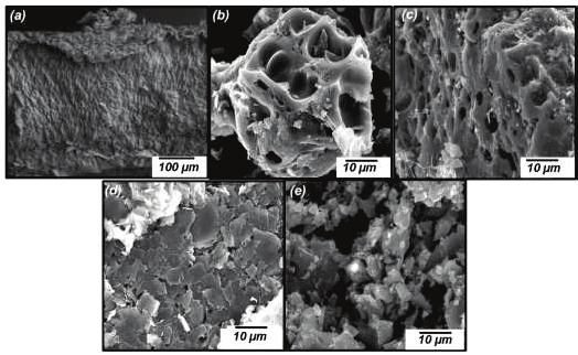
165 143
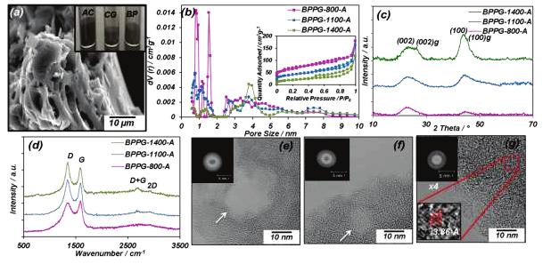
166 144
167 Table 5.1: Structure and textural properties of BPPG and BPPG-A Samples d 002 (Å) L a (nm) L c (nm) I G /I D a S BET (m 2 /g) b V t (cm 3 /g) c pore vol % (<2nm) BPPG BPPG BPPG-1400 BPPG-800- A A BPPG BPPG A 3.84/3.3 5 pore vol % 7.30/ / / / / AC (> 2nm) a I D and I G are the integrated intensities of D- and G-band. b Surface area was calculated with Brunauer_Emmett_Teller (BET) method. c The total pore volume was determined at a relative pressure of Figure 5.2(c) shows the XRD patterns of the BPPG-A specimens. The XRD patterns of the BPPG are shown in Figure 5.3(c). It can be seen that the 300 C activation will not appreciably alter the graphitic order/disorder. The results of the XRD analysis, along with the results of Raman and BET, are shown in Table 5.1. The average graphene interlayer spacing was calculated from the peak centers. The thickness and average width of the graphitic domains, L c and L a, are calculated based on the well-known Scherrer equation, using the FWHM values of (002) at 2θ ~ 23 o and (100) at 2θ ~ 43 o. As Table 5.1 demonstrates, the integraphene layer (d 002 ) spacing gradually shifts toward lower values with increasing carbonization temperature. However, a comparison of the 800 C, 1100 C and 1400 C carbons indicates that this trend is quite weak, and that in all cases the spacing is significantly above that of equilibrium graphite ( nm). In the 800 C and 1100 C specimens the average thickness of the pseudographitic domains is ~ 1.6 nm, indicating that they are composed of ~ 4 stacked graphene layers (i.e., 1.6/0.4 = 4). In the 1400 C specimens the domains are composed of ~ 5 stacked layers. 145
168 . 146
169 147
170 148
171 Table 5.2: XPS results on BPPG and BPPG-A that were mechanically ground after synthesis so as to expose bulk material to surface analysis XPS (After grinding) Samples K Mg P C O N Si Cl [wt%] [wt%] [wt%] [wt%] [wt%] [wt%] [wt%] [wt%] BPPG BPPG BPPG BPPG-800-A BPPG-1100-A BPPG-1400-A Electrochemical performance versus Na We performed cyclic voltammetry (CV) and galvanostatic discharge/charge cycling on both the BPPG and BPPG-A, tested between and 2.8 V vs. Na/Na +. Figures 5.6(a) and 5.6(b) show the CV curves and the galvanostatic discharge/charge profiles for BPPG-1100-A, at cycle 1, 2, 5 and 10. The CV and galvanostatic data for the other materials are shown in Figures 5.7, and 5.8. The inset in Figure 5.6(b) is the dq/dv curve, which has a similar shape to the CVs. Two small reduction peaks at ~0.5 and ~ 0.7 V are observed in the first CV scan and disappeared in the subsequent scans. The formation of a solid electrolyte interface (SEI) would occur at these potentials. However due to the carbons' low surface area, we attribute these two peaks more to irreversible Na insertion into the bulk. Table 5.3 shows the cycle 1 coulombic efficiency (CE) of the BPPG and BPPG-A specimens. There is a notable improvement in the cycle 1 CE with increasing order in the carbons (going from 63% to 73% for 800 C vs C carbonization) but only a marginal decrease in the CE with increased surface area (e.g. dropping to 61% for 800 C + activation). This indicates the cycle 1 irreversible trapping of Na is associated with carbon disorder, be it at the highly defective graphene sites or in the amorphous regions between the pseudographitic domains. However during steady state cycling the CE is 100%, hence minimal additional permanent trapping of Na occurs. 149
172 A pair of highly reversible (minimal voltage hysteresis) oxidation/reduction peaks are present at V, similar to lithium insertion in graphite. 5,7 As Table 5.4 points out, at an intermediate charging rate (50 ma/g) the reversible capacity of the as-carbonized and the activated specimens is very similar. For instance, for BPPG-1100 versus BPPG-1100-A the total capacity difference is 23 mah/g (362 mah/g vs. 385 mah/g). As Figure 5.6(c) shows, all the BPPG and BPPG-A display a sloping-voltage region, and a nearly flat plateau at potentials lower than 0.2 V. The effect of carbonization temperature on the fraction of the total capacity associated with the plateau below 0.1 V is summarized in the histogram shown in Figure 5.6(d). The sub-0.1 V capacities increase with higher degree of ordering, being 106 mah/g for BPPG- 800-A, 200 mah/g for BPPG-1100-A and 238 mah/g for BPPG-1400-A. The low voltage capacity is fully independent of activation, indicating that it is not due to nanopore filling by Na metal, aka "nanoplating". Charge storage in carbons for LIBs and NIBs has been ascribed to the following mechanisms, chemisorption on surface heteroatoms, 80 metal nanopore filling, i.e. "nanoplating", 52,78,81 intercalation between graphene layers, 12,54 and reversible adsorption at structural defect sites in the graphene The charge-discharge profiles in high surface area carbons with high O and N contents have a substantial voltage hysteresis, often being on the order of 1 V or more throughout the entire capacity range. 56,57,80 Below 0.2 V the 1100 C and 1400 C BPPG and BPPG-A have hysteresis that is less than 0.05 V. As we will demonstrate in the subsequent analysis, the key low voltage charge storage mechanism for BPPG is the reversible intercalation of Na between the graphene planes of the pseudographtic domains. In all the BPPG specimens the graphene sheets also contain a high content of defects. We attribute the sloping high voltage charge storage behavior to reversible binding of Na at graphene divacancies defects, as has been recently predicted by ab initio calculations
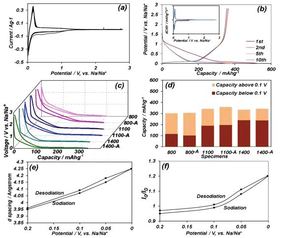
173 151
174 152
175 Table 5.4: Coulombic efficiency and cycling capacity of BPPG and BPPG-A, versus Na. Samples were activated at 0.05 A/g for 10 cycles and were subsequently tested at 0.1 A/g Samples Initial CE (%) Cycle 2 (mah/g) Cycle 50 (mah/g) Cycle 300 (mah/g) BPPG-800 (Na) BPPG-1100 (Na) BPPG-1400 (Na) BPPG-800-A (Na) BPPG-1100-A (Na) BPPG-1400-A (Na) The relatively high density of BPPG also delivers a high volumetric charge capacity. Figure 5.9 provides this result for BPPG-1100-A, as a function of cycle number. For all experiments we employed a mass loading of ~1 mg cm -2 giving an average electrode thickness of 14 µm (see cross section SEM image in Figure 5.9). This results in an electrode with a packing density of ~ 0.75 g cm -3. Thus the reversible volumetric capacity obtained for BPPG A is ~ 700 mah cm -3 by active material (i.e. based on the true density of the carbon), and ~ 270 mah cm -3 by electrode volume. It is difficult to make a one-to-one volumetric comparison with commercial LIB graphite since professionally manufactured commercial electrodes are both thicker (with correspondingly higher mass loading) and are roll-pressed rather than drop cast onto a current collector. The details of manufacturing process are almost always proprietary. However, it is possible to increase the packing density and the mass loading of BPPG to be closer to commercial systems. We employed a Carver TM laboratory press (4000 psi) to achieve electrodes with a mass loading of ~ 6.2 mg. The resultant electrode thickness was 39 µm on a geometric area of 1.54 cm 2. This electrode is also shown in Figure
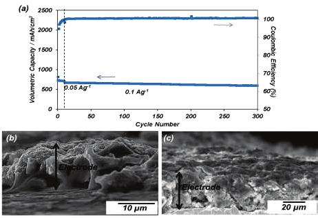
176 154
177 (~330 mah/g), the stoichiometric factor x in Na x C 6 is ~ Examining the interlayer upon subsequent desodiation indicates that the process is highly reversible, agreeing with the electrochemical testing. As indicated by the Raman spectra (Figure 5.6(f)), BPPG-1400-A becomes progressively more ordered during sodiation and subsequently disordered during the reverse process. Similar to the XRD results, the ordering is highly reversible with voltage. This Na insertion-induced ordering phenomena has not been previously reported. Neither XRD nor XPS show evidence of Na metal nanopore filling even at V. Metal peaks were not detected in the XRD patterns for any of the BPPG. We followed the XPS - scotch tape methodology employed in ref. 84 to analyze Na bonding in the interior of BPPG A. The C1s spectrum shown in Figure 5.10(d) shows minimal (Na)carbonates, indicating that the SEI layer was successfully removed along with the top of the carbon. Figure 5.10(c) demonstrates a strong binding peak of Na at ev, which almost entirely disappears at 2.8 V. We attribute this peak to C - Na bonds within the pseudographitic domains, although prior experimental evidence for this interpretation is unavailable. The binding energy for metallic sodium is ev, while for Na 2 O it is ev, both of which are conspicuously absent. The fact that the Na signal almost entirely disappears at 2.8 V is also a strong indication that the SEI is removed. XPS results on samples without using the scotch tape approach show a strong peak in Na 1s spectra at ~1071 ev at both and 2.8 V but with lower signal intensity after desodiation to 2.8 V. This indicates that some of the decomposition products that are formed can be partially dissolved. The presence of considerable (Na)carbonate peaks after desodiation to 2.8 V in both Na 1s and C 1s spectra indicates that these peaks could be related to the decomposition products rather than Na inside the electrode. This was further confirmed by SEM images of electrodes after desodiation to 2.8 V before and after using the scotch tape method (Figure 5.11). The morphology of the electrode after using the scotch tape method is almost identical to the as-prepared one with clean surfaces and sharp boundaries. By contrast, without using this method the surface is no longer smooth but rather rough in appearance with SEI layer covering the surface. 155
-(f) High resolution Na 1s, and C 1s XPS spectra for sodiated and desodiated BPPG-1400-A, analyzed after 10 cycles. 5.10(c) and 5.")
178 (a) XRD spectra for BPPG-1400-A at different discharge and charge voltages versus Na. (b) Raman spectra for BPPG-1400-A at different discharge and charge voltages versus Na. (c)-(f) High resolution Na 1s, and C 1s XPS spectra for sodiated and desodiated BPPG-1400-A, analyzed after 10 cycles. 5.10(c) and 5.10(d) show spectra for samples where the electrode's top SEI covered surface was removed by the scotch tape method. 5.10(e) and 5.10(f) show spectra for samples without the top layer removed, i.e. intact electrode covered by SEI. 156
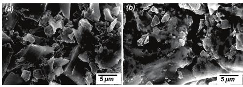
179 157
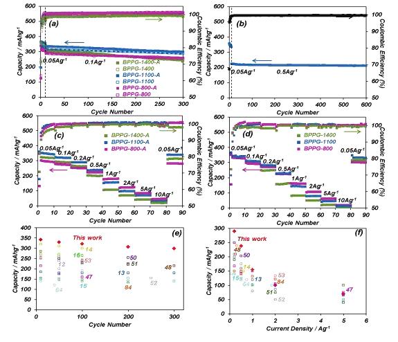
180 158
181 (b) Extended cycling performance and CE of the BPPG-1100-A electrode. (c) Rate performance of BPPG-A electrodes. (d) Rate performance of BPPG electrodes. (e) (f) Cycling capacity retention and rate capability comparison of BPPG-1100-A with the state-of-the-art in literature, tested versus Na. Red diamonds are our results. The introduction of limited micro and mesoporosity into the BPPG is therefore essential for reducing the solid diffusional limitations by creating carbon walls that are in effect much thinner than their macroscopic dimensions. At high rates every activated carbon (SA's of m 2 g -1 ) outperforms its unactivated counterpart (SA's of m 2 g -1 ). Among the ascarbonized materials BPPG-800 demonstrates the highest surface area (33 m 2 g -1 ) and rate performance, while BPPG-1400 shows the lowest surface area (14.5 m 2 g -1 ) and rate performance. Electrochemical impedance spectroscopy (EIS) was employed to further examine the cycling behavior of BPPG-A and BPPG specimens. The impedance spectra of the electrodes before and after cycling were modeled, with the equivalent circuit depicted in Figure Figure 5.14 shows the Nyquists plots for samples before cycling and after 300 cycles, respectively. The spectra consist of a depressed semicircle in the high- and middle-frequency regions and a straight line in the low-frequency region. R el represents the sum of electrical resistances (contacts, etc.), C dl the electrical double layer capacitance, R ct is the charge transfer resistance and Z W Warburg-type element associated with ion diffusion in the carbon electrode. For the cycled electrodes an additional parallel combination of a resistor and capacitor are added to represent ion transport through the SEI layer, 89 denoted as R f and C f, respectively. The numerical values obtained from modeling are listed in Table 5.5. Figure 5.13: Equivalent electronic circuits used to simulate the electrochemical impedance 159
182 160
183 BPPG-800 (Na) BPPG-1100 (Na) BPPG-1400 (Na) BPPG-800-A (Li) BPPG-1100-A (Li) BPPG-1400-A (Li) BPPG-800 (Li) BPPG-1100 (Li) BPPG-1400 (Li) For the as-prepared samples, the trend in the charge transfer resistance, which is roughly equal to the diameter of the semicircle in the spectra, indicates that the lower carbonization temperature gives higher charge transfer resistance (Figure 5.14(a)-(b)). After 300 cycles the charge transfer resistance is substantially larger for BPPG-1400-A and BPPG-1400 specimens (Figure 5.14(c) and Table 5.5), supporting the argument that the samples' inferior cycling coulombic efficiency is associated with higher rates of SEI formation. The cycling-induced increase in the charge transfer resistance is on par for the BPPG-1100-A and BPPG-800-A specimens. However the total charge transfer resistance of BPPG-800-A remains higher than for BPPG-1100-A, an effect probably associated with the underlying structure of the carbon. It is plausible that Na insertion into a more disordered carbon from the electrolyte will be less facile than for a more ordered counterpart. Thus there would be a higher charge transfer resistance both in the as-synthesized state, before there is any SEI, and after extensive cycling. As Figure 5.15(e) indicates, past the first several charge/discharges, the cycling induced increase in the charge transfer resistance in both BPPG-1100-A and BPPG-800-A is quite minimal. A comparison of the performance of the BPPG-1100-A specimen with state-of-the-art carbons is presented in Table 5.6 and in Figures 5.12(e) and 5.12(f). Figures 5.12(e) and 5.12(f) show the cycling performance and the rate capability comparison, respectively, with the solid red diamonds being our results. Table 5.6 emphasizes the plateau capacity (below 0.1 V) comparison of BPPG-1100-A with literature, an essential metric not captured in the total capacity plots presented in Figures 5.12(e) and 5.12(f). Carbons included in the comparison are carbon nanosheets, 52 carbon nanofibers, 13,16,53,57,80 hard carbon, 12,14 templated carbon, 64 highly 161
 200 mag -1 At 50 mag -1 (10 th Cyclability (discharge capacity) 342 mahg -1 at 11 th cycle 298 mahg -1 at 300 th cycle Rate performance 290")
184 Material BPPG-1100-A (this work) Initial coulombic efficiency (%) 67.8 Plateau capacity (capacity below 0.1 V vs Na/Na + ) 200 mag -1 At 50 mag -1 (10 th Cyclability (discharge capacity) 342 mahg -1 at 11 th cycle 298 mahg -1 at 300 th cycle Rate performance 290 mahg -1 at 200 mag mahg -1 at 500 mag
185 cycle) 88% capacity retention over 290 cycles at 100 mag mahg -1 at 1 Ag mahg -1 at 2 Ag mahg -1 at 5 Ag -1 Carbon Nanosheets (Ref. 56) 34.8 ca. 40 mahg -1 at 50mAg -1 (10 th cycle) ca. 260 mahg -1 at 10 th cycle ca. 155 mahg -1 at 200 th cycle 60% retention over 190 cycles at 50 mag -1 ca. 190mAhg -1 at 200mAg -1 ca. 125mAhg -1 at 500mAg -1 ca. 80 mahg -1 at 1Ag mahg -1 at 2 Ag mahg -1 at 5 Ag -1 Interconnected Carbon nanofibers (Ref. 80) 41.8 Not reported 151 mahg -1 at 10 th cycle mahg -1 at 200 th cycle 88.7% retention over 190 cycles at 200mAg mahg -1 at 200 mag mahg -1 at 500 mag mahg -1 at 1 Ag mahg -1 at 2 Ag mahg -1 at 5 Ag -1 Hard carbon particles (Ref. 12) 78 ca. 150 mahg -1 at 25mAg mahg -1 at 2 nd cycle 225 mahg -1 at 100 th cycle 88% retention over 98 cycles at 25 mag -1 Not reported Templated carbon (Ref. 64) 20 ca. 20 mahg -1 at 74mAg -1 (10 th cycle) 180 mahg -1 at 2 nd cycle, 120 mahg -1 at 40 th cycle 66.7% retention over 38 cycles at 74 mag -1 ca.140mahg -1 at 74mAg -1 ca.120mahg -1 at 740mAg -1 ca. 100mAhg -1 at 1.85 Ag -1 Carbon fibers (Ref. 57) 46 Not reported ca. 350 mahg -1 at 2 nd cycle 243 mahg -1 at 100 th cycle 70% retention over 98 cycles at 50 mahg mahg -1 at 200 mag mahg -1 at 500 mag mahg -1 at 1Ag mahg -1 at 2 Ag mahg -1 at 5 Ag -1 Highly disordered carbon (Ref. 55) 57.6 ca. 110 mahg -1 at 100 mag -1 (3 rd cycle) 255 mahg -1 at initial cycles 234 mahg -1 at 180 th 92% retention over 170 cycles at 100 mag mahg -1 at 200 mag mahg -1 at 500 mag mahg -1 at 1 Ag mahg -1 at 2 Ag mahg -1 at 5 Ag -1 Hollow carbon Nanowires (Ref. 52) 50.5 ca. 150 mahg -1 at 50mAg -1 (10 th cycle) ca. 255 mahg -1 at 10 th cycle ca. 220 mahg -1 at 200th cycle 86% retention over 190 cycles at 50 mag mAhg-1 at 250 mag mahg -1 at 500mAg -1 Hollow carbon nanospheres (Ref. 51) 41.5 ca. 20 mahg -1 at 50 mag -1 (10 th cycle) 250 mahg -1 at 10th cycle, 160 mahg -1 at 100th cycle 64% retention over 90 cycles at 100mAg mAhg -1 at 200mAg mAhg -1 at 500mAg mahg -1 at 1Ag mAhg -1 at 2Ag -1 75mAhg -1 at 5Ag -1 Carbonized peat moss (Ref. 54) mahg -1 at 50 mag -1 (10 th cycle) 284 mahg -1 at 11 th cycle 255 mahg -1 at 210 th cycle 90% retention over 200 cycles at 100 mag mahg -1 at 200 mag mahg -1 at 500 mag mahg -1 at 1Ag mahg -1 at 2Ag
186 66 mahg -1 at 5Ag -1 Carbon nanofibers (Ref. 13) Nanocellular carbon foams (Ref. 15) Porous carbon nanofiber (Ref. 16) Carbon fibers (Ref. 53) Hard carbon (Ref. 14) 58.7 Not reported 53.5 ca. 130 mahg -1 at 40 mag -1 (10 th cycle) Not reported ca. 170 mahg -1 at 50 mag -1 (10 th cycle) 200 mahg -1 at 2 nd cycle 180mAhg -1 at 300 th cycle 90% retention over 298 cycles at 200mAg mahg -1 at 2 nd cycle 137mAhg -1 at 300 th cycle 90% retention over 298 cycles at 100mAg mah g -1 at 10 th cycle 266 mah g -1 at 100 th cycle 95% retention over 90 cycles at 50 mag mahg -1 at 200 mag mahg -1 at 500 mag mahg -1 at 1 Ag mahg -1 at 2 Ag mahg -1 at 200mAg mahg -1 at 500mAg mahg -1 at 1Ag mahg -1 at 5Ag mahg -1 at 500mAg mahg -1 at 1Ag mahg -1 at 2Ag mahg -1 at 5Ag -1 < mah g -1 (1 st cycle) Not reported Not reported 61 >170 mah g -1 (1 st cycle) 340 mah g -1 at 2 nd cycle 300mAh g -1 at 120 th cycle 88% retention over118 cycles at ~30mA g mahg -1 at ~60mAg mahg -1 at ~300mAg mahg -1 at ~600mAg Electrochemical performance versus Li The dense BPPG carbons are also uniquely promising for LIB applications, as the highly defective graphene sheets within the pseudographic domains will reversibly bind with Li, while the near-surface nanopores will provide sites for underpotential metal deposition. Figure 5.16(a) shows the cycling performance of the BPPG-A electrodes, with the coulombic efficiency of the electrodes also being displayed. The cycling CE is close to 100%. Figure 5.16(b) shows the rate performance of BPPG-1100-A electrode. BPPG-800-A, which is the most disordered carbon, demonstrated by far the highest overall cycling capacity, being at 800 mah/g at cycle 300 when tested at 100 ma/g. This is direct evidence for the necessity of graphene defects in achieving a reversible capacity with Li that far surpasses that of commercial graphite. It has been shown that a divacancy is the thermodynamically most stable defect preferential Li adsorption site , 90, 91 and will also act as a The CV curve of the BPPG-1100-A specimens is shown in Figure 5.17(a). Lithiation/delithiation demonstrates a pronounced reduction peak at 0-1 V during the 1 st cycle and at V during the subsequent cycles. The discharge - charge profiles for BPPG-A and BPPG are shown in Figures 5.17 and The initial CEs are slightly lower when employing Li (Table 5.7) rather than Na (Table 5.4), which may be accounted for the difference in the 164
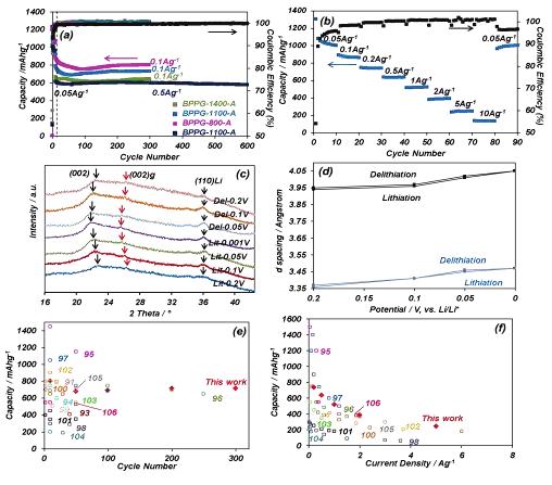
187 165
188 166
189 167
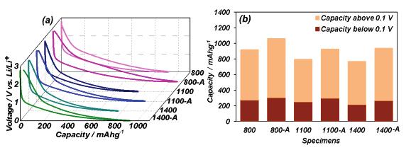
190 168
191 169
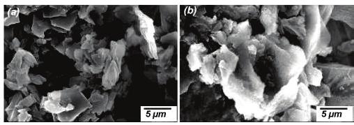
192 170
ALD TiO 2 coated Silicon Nanowires for Lithium Ion Battery Anodes with enhanced Cycling Stability and Coulombic Efficiency
 ALD TiO 2 coated Silicon Nanowires for Lithium Ion Battery Anodes with enhanced Cycling Stability and Coulombic Efficiency Elmira Memarzadeh Lotfabad a, Peter Kalisvaart a,*, Kai Cui b, Alireza Kohandehghan
Supporting Information. Peanut Shell Hybrid Sodium Ion Capacitor with Extreme. Energy - Power Rivals Lithium Ion Capacitors
 Electronic Supplementary Material (ESI) for Energy & Environmental Science. This journal is The Royal Society of Chemistry 214 Supporting Information Peanut Shell Hybrid Sodium Ion Capacitor with Extreme
High Rate and Durable, Binder Free Anode Based on Silicon Loaded MoO 3 Nanoplatelets
 Supplementary Information High Rate and Durable, Binder Free Anode Based on Silicon Loaded O 3 Nanoplatelets Alejandro Martinez-Garcia, Arjun Kumar Thapa,Ruvini Dharmadasa,, Tu Q. Nguyen, Jacek Jasinski,
6th International Conference on Advanced Design and Manufacturing Engineering (ICADME 2016)
") 6th International Conference on Advanced Design and Manufacturing Engineering (ICADME 2016) Porous Co3O4 irregular Micro-cubes with lithium storage performances Ting Wanga, Hao Zhengb, Jinsong Chengc,
6th International Conference on Advanced Design and Manufacturing Engineering (ICADME 2016) Porous Co3O4 irregular Micro-cubes with lithium storage performances Ting Wanga, Hao Zhengb, Jinsong Chengc,
Supplementary Information
 Supplementary Information Supplementary Figure 1 Characterization of precursor coated on salt template. (a) SEM image of Mo precursor coated on NaCl. Scale bar, 50 μm. (b) EDS of Mo precursor coated on
Investigation of anode materials for lithium-ion batteries
 University of Wollongong Thesis Collections University of Wollongong Thesis Collection University of Wollongong Year 2006 Investigation of anode materials for lithium-ion batteries Ling Yuan University
High Performance Lithium Battery Anodes Using Silicon Nanowires
 Supporting Online Materials For High Performance Lithium Battery Anodes Using Silicon Nanowires Candace K. Chan, Hailin Peng, Gao Liu, Kevin McIlwrath, Xiao Feng Zhang, Robert A. Huggins and Yi Cui * *To
Carbon-Silicon Core-Shell Nanowires as High Capacity Electrode for Lithium Ion Batteries
 Carbon-Silicon Core-Shell Nanowires as High Capacity Electrode for Lithium Ion Batteries NANO LETTERS XXXX Vol. xx, No. x - Li-Feng Cui, Yuan Yang, Ching-Mei Hsu, and Yi Cui* Department of Materials Science
Micron-Sized Nanoporous Antimony with Tunable Porosity for. High Performance Potassium-Ion Batteries
 1 Micron-Sized Nanoporous Antimony with Tunable Porosity for High Performance Potassium-Ion Batteries Yongling An, Yuan Tian, Lijie Ci, Shenglin Xiong, Jinkui Feng,*, Yitai Qian SDU & Rice Joint Center
Investigation of anode materials for lithium-ion batteries
 University of Wollongong Thesis Collections University of Wollongong Thesis Collection University of Wollongong Year 2006 Investigation of anode materials for lithium-ion batteries Ling Yuan University
SUPPLEMENTARY INFORMATION
 In the format provided by the authors and unedited. DOI: 10.1038/NNANO.2017.27 Revealing the reaction mechanisms of Li-O 2 batteries using environmental transmission electron microscopy Langli Luo, Bin
Supplementary Figure 1. Crystal structures of conventional layered and Li-rich layered manganese oxides. a, The crystal structure of rhombohedral
 Supplementary Figure 1. Crystal structures of conventional layered and Li-rich layered manganese oxides. a, The crystal structure of rhombohedral LiMO 2 (M = Ni, Co, Mn) with the space group R3m. b, The
Dramatically enhanced reversibility of Li 2 O in SnO 2 -based electrodes: the effect of nanostructure on high initial reversible capacity
 Electronic Supplementary Material (ESI) for Energy & Environmental Science. This journal is The Royal Society of Chemistry 2015 Electronic supplementary information for Dramatically enhanced reversibility
Microscopic Structural Analysis of Advanced Anode Material for Lithium Battery
 JFE TECHNICAL REPORT No. 22 (Mar. 2017) Microscopic Structural Analysis of Advanced Anode Material for Lithium Battery SIMAUCHI Yutaka *1 OHMORI Shigekazu *2 IKEMOTO Sachi *3 Abstract: analyzed the microstructure
De-ionized water. Nickel target. Supplementary Figure S1. A schematic illustration of the experimental setup.
 Graphite Electrode Graphite Electrode De-ionized water Nickel target Supplementary Figure S1. A schematic illustration of the experimental setup. Intensity ( a.u.) Ni(OH) 2 deposited on the graphite blank
Supplementary Figure 1. Photographs of the Suaeda glauca (S. glauca) Bunge at different stages of metal ion absorption. (a) Photographs of S.
 Bunge at different stages of metal ion absorption. (a) Photographs of S.") 1 2 3 4 5 6 7 Supplementary Figure 1. Photographs of the Suaeda glauca (S. glauca) Bunge at different stages of metal ion absorption. (a) Photographs of S. glauca after absorption of tin salt. (b) Photographs
1 2 3 4 5 6 7 Supplementary Figure 1. Photographs of the Suaeda glauca (S. glauca) Bunge at different stages of metal ion absorption. (a) Photographs of S. glauca after absorption of tin salt. (b) Photographs
Enhancement of connectivity and flux pinning in MgB2 superconducting bulks and wires
 University of Wollongong Research Online University of Wollongong Thesis Collection 1954-2016 University of Wollongong Thesis Collections 2009 Enhancement of connectivity and flux pinning in MgB2 superconducting
State Key Laboratory of Advanced Electromagnetic Engineering and Technology, School of
 Electronic Supplementary Material (ESI) for Nanoscale. This journal is The Royal Society of Chemistry 2018 Electrocatalysis of polysulfide conversion by conductive RuO 2 Nano Dots for lithium sulfur batteries
Rice husks as a sustainable source of nanostructured silicon for high performance Li-ion battery anodes
 Supplementary Information Rice husks as a sustainable source of nanostructured silicon for high performance Li-ion battery anodes Nian Liu 1, Kaifu Huo 2,3, Matthew T. McDowell 2, Jie Zhao 2 & Yi Cui 2,4
In situ generation of Li 2 FeSiO 4 coating on MWNT as a high rate cathode material for lithium ion batteries
 Supporting Information: In situ generation of Li 2 FeSiO 4 coating on MWNT as a high rate cathode material for lithium ion batteries Yi Zhao, Jiaxin Li, Ning Wang, Chuxin Wu, Yunhai Ding, Lunhui Guan*
Safe, Inexpensive, Long Life, High Power and Efficiency Batteries For Grid Scale Energy Storage Applications
 Safe, Inexpensive, Long Life, High Power and Efficiency Batteries For Grid Scale Energy Storage Applications Investigators Yi Cui, Associate Professor; Robert Huggins, Professor; Mauro Pasta, Postdoctoral
School of Materials Science and Engineering, South China University of Technology,
 Supporting information Zn/MnO 2 Battery Chemistry With H + and Zn 2+ Co-Insertion Wei Sun, Fei Wang, Singyuk Hou, Chongyin Yang, Xiulin Fan, Zhaohui Ma, Tao Gao, Fudong Han, Renzong Hu, Min Zhu *, Chunsheng
Sn Wears Super Skin: A New Design For Long Cycling Batteries
 Supporting Information Wears Super Skin: A New Design For Long Cycling Batteries Shuai Kang, Xi Chen, Junjie Niu* Department of Materials Science and Engineering, CEAS, University of Wisconsin-Milwaukee
measurements. The spectra show electrolyte in contact with the carbon fibre based gas diffusion layer
 Supplementary Figure 1. 7 Li NMR spectra of electrolyte in contact with potential substrates for in-situ NMR measurements. The spectra show electrolyte in contact with the carbon fibre based gas diffusion
SUPPLEMENTARY INFORMATION
 SUPPLEMENTARY INFORMATION SUPPLEMENTARY DISCUSSION AND FIGURES 1. Chemical and Structural Characterization (a) Grazing-incidence small-angle X-ray scattering (GISAXS) The structural evolution of the mesoporous
The Preparation of C/Ni Composite Nanofibers with Pores by Coaxial Electrospinning
 2016 International Conference on Intelligent Manufacturing and Materials (ICIMM 2016) ISBN: 978-1-60595-363-2 The Preparation of C/Ni Composite Nanofibers with Pores by Coaxial Electrospinning Yiqiang
Carbon Nanotube-Based Supercapacitors with Excellent AC-Line
 SUPPORTING INFORMATION FOR: Carbon Nanotube-Based Supercapacitors with Excellent AC-Line Filtering and Rate Capability via Improved Interfacial Impedance Yverick Rangom, Xiaowu (Shirley) Tang*, and Linda
Lithium Batteries with Nearly Maximum Metal. Storage Supporting Information
 Lithium Batteries with Nearly Maximum Metal Storage Supporting Information Abdul-Rahman O. Raji,, Rodrigo Villegas Salvatierra,, Nam Dong Kim, Xiujun Fan, Yilun Li, Gladys A. L. Silva, Junwei Sha and James
image of ZMO precursor/rgo. Scale bar, 50 nm. (b) XRD patterns of reduced graphene
 XRD patterns of reduced graphene") Supplementary Figures Supplementary Figure 1 Characterization of ZMO precursor/rgo. (a) STEM image of ZMO precursor/rgo. Scale bar, 50 nm. (b) XRD patterns of reduced graphene oxide (rgo) and ZMO precursor/rgo.
Supplementary Figures Supplementary Figure 1 Characterization of ZMO precursor/rgo. (a) STEM image of ZMO precursor/rgo. Scale bar, 50 nm. (b) XRD patterns of reduced graphene oxide (rgo) and ZMO precursor/rgo.
Application in High-Performance Lithium-
 Solution Ionic Strength Engineering as a Generic Strategy to Coat Graphene Oxide (GO) on Various Functional Particles and Its Application in High-Performance Lithium- Sulfur (Li-S) Batteries Jiepeng Rong,Mingyuan
Supporting Information
 Electronic Supplementary Material (ESI) for Energy & Environmental Science. This journal is The Royal Society of Chemistry 2018 Supporting Information High performance All-Solid-State Li-Se Batteries induced
Elucidating the Phase Transformation of Li4Ti5O12 Lithiation at the Nanoscale
 Elucidating the Phase Transformation of Li4Ti5O12 Lithiation at the Nanoscale Michael G. Verde 1*, Loïc Baggetto 2, Nina Balke 3, Gabriel M. Veith 2, Joon Kyo Seo 4, Ziying Wang 1, Ying Shirley Meng 1*
Urchin-like V 2 O 3 /C Hollow Nanospheres Hybrid for High-Capacity and Long-Cycle-Life Lithium Storage
 Supporting Information Urchin-like V 2 O 3 /C Hollow Nanospheres Hybrid for High-Capacity and Long-Cycle-Life Lithium Storage Peng Yu, Xu Liu, Lei Wang,* Chungui Tian, Haitao Yu, and Honggang Fu* Key Laboratory
Tailor Made Carbon and Graphite Based Anode Materials for Lithium Ion Batteries. Heribert Walter, Battery+Storage 2013
 Tailor Made Carbon and Graphite Based Anode Materials for Lithium Ion Batteries Heribert Walter, Battery+Storage 2013 Agenda SGL Group at a Glance Anode Materials Overview Material Synthesis and Modification
Supplementary Figure 1:
 b a c Supplementary Figure 1: Calibration of the Cs + sputtering rate on composite LiNi 0.7 Mn 0.15 Co 0.15 O 2 electrodes (500 ev ion energy, ~40 na measured sample current): (a) Optical profilometry
Amorphous and Nanocrystalline Mg 2 Si Thin Film Electrodes
 Manuscript# IMLB-070, LBNL-52142 Revised to Journal of Power Sources (Dec 13, 2002) Amorphous and Nanocrystalline Mg 2 Si Thin Film Electrodes Seung-Wan Song, a Kathryn A. Striebel, a,z Xiangyun Song a
Rapid degradation of methylene blue in a novel
 Title: Rapid degradation of methylene blue in a novel heterogeneous Fe 3 O 4 @rgo@tio 2 -catalyzed photo-fenton system Author names Xiaoling Yang, Wei Chen, Jianfei Huang, Ying Zhou, Yihua Zhu,* and Chunzhong
Supplementary Figure 1 The lithium polysulfide distribution on the patterned electrode.
 Supplementary Figure 1.The lithium polysulfide distribution on the patterned electrode. SEM image of the ITO-carbon electrode after dipping into Li 2 S 8 solution and drying, which shows the random distribution
Kuang-Che Hsiao. Supervisor: Prof. Tony West
 New Potential Cathode Materials for Lithium-ion ion Battery - Synthesis and characterization of Li 1+x FePO 4-x N x cathode - Kuang-Che Hsiao Supervisor: Prof. Tony West 08/06/2010 E-mail: dtp09kh@sheffield.ac.uk
Supporting Information
 Electronic Supplementary Material (ESI) for Journal of Materials Chemistry A. This journal is The Royal Society of Chemistry 2014 Supporting Information Hierarchical Orthorhombic V 2 O 5 Hollow Nanospheres
Corrosion. Lab. of Energy Conversion & Storage Materials. Produced by K. B. Kim
 Corrosion 대기환경에의한금속소재 (organic film coated steel) 의퇴화현상평가연구 Lab. of Energy Conversion & Storage Materials Produced by K. B. Kim Introduction AC Impedance Spectroscopy Application of AC Impedance to Corrosion
Supplementary Figures
 Supplementary Figures Supplementary Figure 1. (a) XRD patterns of mesoporous silica template, KIT-6, and mesoporous MoO2 obtained by nano-replication method. The KIT-6 template exhibits typical XRD peaks
Silver Diffusion Bonding and Layer Transfer of Lithium Niobate to Silicon
 Chapter 5 Silver Diffusion Bonding and Layer Transfer of Lithium Niobate to Silicon 5.1 Introduction In this chapter, we discuss a method of metallic bonding between two deposited silver layers. A diffusion
Supporting Information. Multistep Lithiation of Tin Sulfide: An Investigation Using in Situ Electron
 Supporting Information Multistep Lithiation of Tin Sulfide: An Investigation Using in Situ Electron Microscopy Sooyeon Hwang, Zhenpeng Yao, Lei Zhang, Maosen Fu,, Kai He, Liqiang Mai, Chris Wolverton,
Doped Si nanoparticles with conformal. and high-rate lithium-ion battery anodes
 Nanotechnology Nanotechnology 26 (2015) 365401 (6pp) doi:10.1088/0957-4484/26/36/365401 Doped Si nanoparticles with conformal carbon coating and cyclizedpolyacrylonitrile network as high-capacity and high-rate
Schottky Tunnel Contacts for Efficient Coupling of Photovoltaics and Catalysts
 Schottky Tunnel Contacts for Efficient Coupling of Photovoltaics and Catalysts Christopher E. D. Chidsey Department of Chemistry Stanford University Collaborators: Paul C. McIntyre, Y.W. Chen, J.D. Prange,
Nanowire Arrays and 3D Porous Conducting Networks for Li-Ion Battery Electrodes
 University of Colorado, Boulder CU Scholar Mechanical Engineering Graduate Theses & Dissertations Mechanical Engineering Spring 1-1-2014 Nanowire Arrays and 3D Porous Conducting Networks for Li-Ion Battery
Supplementary Figure 1: Sketch of XRD-EIS pouch cell design with Titanium current collectors serving as XRD windows, parafilm, kapton tape made from
 Supplementary Figure 1: Sketch of XRD-EIS pouch cell design with Titanium current collectors serving as XRD windows, parafilm, kapton tape made from polyimide used to seal Titanium (Ti) current collectors
Supporting Information. Carbon Welding by Ultrafast Joule Heating
 Supporting Information Carbon Welding by Ultrafast Joule Heating Yonggang Yao, 1,(a) Kun Fu, 1,(a) Shuze Zhu, 2 Jiaqi Dai, 1 Yanbin Wang, 1 Glenn Pastel, 1 Yanan Chen, 1 Tian Li, 1 Chengwei Wang, 1 Teng
Summary Chapter Chapter Chapter
 Ceria (CeO 2 ) has been extensively employed as an important component of automotive three-way catalysts (TWC) for reducing the exhaust pollutants. Besides this, fuel cell processes, oxygen permeation
Enhanced supercapacitor performance of 3D architecture tailored using atomically thin rgo-mos 2 2D sheets
 Electronic Supplementary Material (ESI) for RSC Advances. This journal is The Royal Society of Chemistry 2016 Electronic Supplementary Information Enhanced supercapacitor performance of 3D architecture
Unlocking the Potential of Amorphous Red Phosphorus Films as Long-term Stable. Negative Electrode for the Lithium Battery
 Electronic Supplementary Material (ESI) for Journal of Materials Chemistry A. This journal is The Royal Society of Chemistry 2016 Supporting Information Unlocking the Potential of Amorphous Red Phosphorus
Supplementary Information
 Electronic Supplementary Material (ESI) for Sustainable Energy & Fuels. This journal is The Royal Society of Chemistry 2018 Supplementary Information for Chemical Science, DOI: 10.1039/ ((please add manuscript
CHAPTER-VII SUMMARY AND CONCLUSIONS
 CHAPTER-VII SUMMARY AND CONCLUSIONS Chapter-VII Summary and Conclusions Sr. No. Title Page No. 7.1 Summary 167 7.2 Conclusions.. 171 CHAPTER SEVEN Summary and Conclusions 7.1: Summary The technologies
Supporting Information. Amorphous Red Phosphorus Embedded in Highly Ordered. Mesoporous Carbon with Superior Lithium and Sodium Storage.
 Supporting Information Amorphous Red Phosphorus Embedded in Highly Ordered Mesoporous Carbon with Superior Lithium and Sodium Storage Capacity Weihan Li, Zhenzhong Yang, Minsi Li, Yu Jiang, Xiang Wei,
Effect of heat treatment on electrochemical characteristics of spinel lithium titanium oxide
 Korean J. Chem. Eng., 27(1), 91-95 (2010) DOI: 10.1007/s11814-009-0298-0 RAPID COMMUNICATION Effect of heat treatment on electrochemical characteristics of spinel lithium titanium oxide Sung-Chul Hong*,
Supporting information
 Electronic Supplementary Material (ESI) for Energy & Environmental Science. This journal is The Royal Society of Chemistry 2015 Supporting information A Low Temperature Molten Salt Process for Aluminothermic
Supplementary Materials for
 advances.sciencemag.org/cgi/content/full/4/3/eaap7970/dc1 Supplementary Materials for In situ formation of molecular Ni-Fe active sites on heteroatom-doped graphene as a heterogeneous electrocatalyst toward
A novel rechargeable battery with magnesium anode, titanium dioxide cathode, and magnesim borohydride/tetraglyme electrolyte
 Electronic Supplementary Material (ESI) for ChemComm. This journal is The Royal Society of Chemistry 2015 A novel rechargeable battery with magnesium anode, titanium dioxide cathode, and magnesim borohydride/tetraglyme
Supporting Information
 Supporting Information Low-Temperature Molten-Salt Production of Silicon Nanowires by the Electrochemical Reduction of CaSiO 3 Yifan Dong, Tyler Slade, Matthew J. Stolt, Linsen Li, Steven N. Girard, Liqiang
Topic: Electrochemical Application of Carbon Materials MILD-EXFOLIATED GRAPHITE AS AN ANODE MATERIAL FOR LITHIUM ION BATTERY.
 Paper ID: 373 Topic: Electrochemical Application of Carbon Materials MILD-EXFOLIATED GRAPHITE AS AN ANODE MATERIAL FOR LITHIUM ION BATTERY Lin Zou, Yong-Ping Zheng, Feiyu Kang, Wanci Shen, Can Xu Laboratory
SUPPORTING INFORMATION. A Rechargeable Aluminum-Ion Battery Based on MoS 2. Microsphere Cathode
 SUPPORTING INFORMATION A Rechargeable Aluminum-Ion Battery Based on MoS 2 Microsphere Cathode Zhanyu Li a, Bangbang Niu a, Jian Liu a, Jianling Li a* Feiyu Kang b a School of Metallurgical and Ecological
Morphology controlled synthesis of monodispersed manganese. sulfide nanocrystals and their primary application for supercapacitor
 Electronic Supplementary Material (ESI) for Chemical Communications. This journal is The Royal Society of Chemistry 2015 Morphology controlled synthesis of monodispersed manganese sulfide nanocrystals
In Situ XRD and TEM Studies of Sol-Gel-based. Synthesis of LiFePO4
 In Situ XRD and TEM Studies of Sol-Gel-based Synthesis of LiFePO4 Dominika A. Ziolkowska a,*, Jacek B. Jasinski b,*, Bartosz Hamankiewicz c, Krzysztof P. Korona a, She-Huang Wu d and Andrzej Czerwinski
Next Generation Anodes for Li-Ion Cells: How to Achieve Both High Capacity and Cycle Stability When Using Silicon Metal
 Next Generation Anodes for Li-Ion Cells: How to Achieve Both High Capacity and Cycle Stability When Using Silicon Metal introduction Jeff Norris CEO +1.803.528.0941 JNorris@ParacleteEnergy.com Michigan
Tin Coated Viral-Nanoforests as Sodium-Ion. Battery Anodes
 Supporting information Tin Coated Viral-Nanoforests as Sodium-Ion Battery Anodes Yihang Liu, Yunhua Xu, Yujie Zhu, James N. Culver, Cynthia A. Lundgren, Kang Xu,*, and Chunsheng Wang*, Sn anodes fabrication:
All-solid-state Li battery using a light-weight solid electrolyte
 All-solid-state Li battery using a light-weight solid electrolyte Hitoshi Takamura Department of Materials Science, Graduate School of Engineering, Tohoku University Europe-Japan Symposium, Electrical
On the Role of Mechanics in the Design and Performance of Electrode Materials for Energy Storage
 On the Role of Mechanics in the Design and Performance of Electrode Materials for Energy Storage Pradeep R. Guduru School of Engineering, Brown University V. Sethuraman, M. Chon, S. Nadimpalli Collaborators:
Supplementary Information. Reversible superconductor-insulator transition in LiTi 2 O 4 induced by
 Supplementary Information Reversible superconductor-insulator transition in LiTi 2 O 4 induced by Li-ion electrochemical reaction K. Yoshimatsu 1,*, M. Niwa 1, H. Mashiko 1, T. Oshima 1 & A. Ohtomo 1,2
Supporting information
 Electronic Supplementary Material (ESI) for Nanoscale. This journal is The Royal Society of Chemistry 2018 Supporting information An amorphous material with sponge-like structure as anode for Liion and
2.4 Secondary Lithium Batteries Lithium-Metal Batteries Lithium-Ion Batteries Lithium Polymer Batteries...
 1 Basic Elements for Energy Storage and Conversion... 1 1.1 Energy Storage Ability... 1 1.2 The Sustained Energy.... 3 1.3 Energy Storage for Nano-electronics................... 4 1.4 Energy Storage...................................
INITIAL STUDY OF THE MICROSTRUCTURE OF CARBON FIBRES ACTING AS NEGATIVE ELECTRODES IN STRUCTURAL BATTERY COMPOSITES
 Munich, Germany, 26-30 th June 2016 1 INITIAL STUDY OF THE MICROSTRUCTURE OF CARBON FIBRES ACTING AS NEGATIVE ELECTRODES IN STRUCTURAL BATTERY COMPOSITES Fang Liu 1, Masoud Rashidi 2 and Leif E. Asp 3
STUDY & ANALYSIS OF ALUMINIUM FOIL AND ANATASE TITANIUM OXIDE (TiO2) USING TRANSMISSION ELECTRON MICROSCOPY
 USING TRANSMISSION ELECTRON MICROSCOPY") STUDY & ANALYSIS OF ALUMINIUM FOIL AND ANATASE TITANIUM OXIDE (TiO2) USING TRANSMISSION ELECTRON MICROSCOPY Ayush Garg Department of Chemical and Materials Engineering, University of Auckland, Auckland,
STUDY & ANALYSIS OF ALUMINIUM FOIL AND ANATASE TITANIUM OXIDE (TiO2) USING TRANSMISSION ELECTRON MICROSCOPY Ayush Garg Department of Chemical and Materials Engineering, University of Auckland, Auckland,
Supporting Information
 Supporting Information Hydrogenation Driven Conductive Na 2 Nanoarrays as Robust Binder-Free Anodes for Sodium-Ion Batteries Shidong Fu, Jiangfeng Ni, Yong Xu, Qiao Zhang*, and Liang Li*, College of Physics,
All Silicon Electrode Photo-Capacitor for Integrated Energy Storage and Conversion
 Supporting Information All Silicon Electrode Photo-Capacitor for Integrated Energy Storage and Conversion Adam P. Cohn 1,, William R. Erwin 3,,, Keith Share 1,2, Landon Oakes 1,2, Andrew S. Westover 1,2,
Supporting Information
 Supporting Information Earth Abundant Fe/Mn-Based Layered Oxide Interconnected Nanowires for Advanced K-Ion Full Batteries Xuanpeng Wang, Xiaoming Xu, Chaojiang Niu*, Jiashen Meng, Meng Huang, Xiong Liu,
Nanocrystalline LiFePO4 as cathode material for lithium battery applications S.C SIAH
 Nanocrystalline LiFePO as cathode material for lithium battery applications Abstract S.C SIAH Engineering Science Programme, National University of Singapore Kent Ridge, Singapore 119260 LiFePO was prepared
Growth of monocrystalline In 2 O 3 nanowires by seed orientation dependent vapour-solid-solid mechanism
 Electronic Supplementary Material (ESI) for Journal of Materials Chemistry C. This journal is The Royal Society of Chemistry 2014 Electronic Supplementary Information (ESI) Growth of monocrystalline In
Superior Additive of Exfoliated RuO 2 Nanosheet. Oxide over Graphene
 Supporting Information Superior Additive of Exfoliated RuO 2 Nanosheet for Optimizing the Electrode Performance of Metal Oxide over Graphene Seul Lee, a, Xiaoyan Jin a, In Young Kim, a Tae-Ha Gu, a Ji-Won
In operandi observation of dynamic annealing: a case. Supplementary Material
 In operandi observation of dynamic annealing: a case study of boron in germanium nanowire devices Supplementary Material Maria M. Koleśnik-Gray, 1,3,4 Christian Sorger, 1 Subhajit Biswas, 2,3 Justin D.
Nano-Confined Metal Oxide in Carbon Nanotube Composite Electrodes for Lithium Ion Batteries
 Florida International University FIU Digital Commons FIU Electronic Theses and Dissertations University Graduate School 3-31-2017 Nano-Confined Metal Oxide in Carbon Nanotube Composite Electrodes for Lithium
SUPPLEMENTARY INFORMATION
 SUPPLEMENTARY INFORMATION Nanoporous Metal/Oxide Hybrid Electrodes for Electrochemical Supercapacitors Xingyou Lang, Akihiko Hirata, Takeshi Fujita, Mingwei Chen * WPI Advanced Institute for Materials
Microstructural Characterization of Materials
 Microstructural Characterization of Materials 2nd Edition DAVID BRANDON AND WAYNE D. KAPLAN Technion, Israel Institute of Technology, Israel John Wiley & Sons, Ltd Contents Preface to the Second Edition
Supporting Information
 Electronic Supplementary Material (ESI) for Journal of Materials Chemistry A. This journal is The Royal Society of Chemistry 2018 Supporting Information Unveiling BiVO 4 Nanorods as a Novel Anode Material
Scalable approach to multi-dimensional bulk Si anodes via metal-assisted chemical etching
 Supplementary Information Scalable approach to multi-dimensional bulk Si anodes via metal-assisted chemical etching Byoung Man Bang, Hyunjung Kim, Hyun-Kon Song, Jaephil Cho* and Soojin Park* Interdisciplinary
Supplementary Figure S1 Crystal structure of the conducting filaments in sputtered SiO 2
 Supplementary Figure S1 Crystal structure of the conducting filaments in sputtered SiO 2 based devices. (a) TEM image of the conducting filament in a SiO 2 based memory device used for SAED analysis. (b)
Enhanced cyclability of Li O 2 batteries with cathodes of Ir and MnO 2 supported on well-defined TiN arrays
 Enhanced cyclability of Li O 2 batteries with cathodes of Ir and MnO 2 supported on well-defined TiN arrays Limin Leng, ab Jing Li, a Xiaoyuan Zeng, a Xinlong Tian, a Huiyu Song, a Zhimin Cui,* a Ting
PHYSICAL REVIEW LETTERS 107,
 Real-time Measurement of Stress and Damage Evolution During Initial Lithiation of Crystalline Silicon M. J. Chon, 1 V.A. Sethuraman, 1 A. McCormick, 1 V. Srinivasan, 2 P. R. Guduru 1,* 1 School of Engineering,
Three-dimensional graphene-based hierarchically porous carbon. composites prepared by a dual-template strategy for capacitive
 Electronic Supplementary Information (ESI) Three-dimensional graphene-based hierarchically porous carbon composites prepared by a dual-template strategy for capacitive deionization Xiaoru Wen, a Dengsong
Formation of High-quality Aluminum Oxide under Ion Beam Irradiation
 15th International School-Conference New materials Materials of innovative energy: development, characterization methods and application Volume 2018 Conference Paper Formation of High-quality Aluminum
EFFECTS OF CURRENT DENSITY ON SIZE AND SURFACE MORPHOLOGY OF HIGH SPEED DIRECT NANO-CRYSTALLINE NICKEL PLATING ON TITANIUM SURFACE
 EFFECTS OF CURRENT DENSITY ON SIZE AND SURFACE MORPHOLOGY OF HIGH SPEED DIRECT NANO-CRYSTALLINE NICKEL PLATING ON TITANIUM SURFACE Noor Zaimah 1, Azieyanti Nurain 1 and Sakhawat Hussain 2 1 Department
From Surface To Cell: Understanding the Lithium Ion Battery. The world leader in serving science
 From Surface To Cell: Understanding the Lithium Ion Battery 1 The world leader in serving science Content Discharge Detail the Li-ion Battery industry drivers & trends Our position in industry and our
Supporting Information. Kirkendall Diffusion, and their Electrochemical Properties for use in Lithium-ion
 Supporting Information Preparation of Hollow Fe 2 O 3 Nanorods and Nanospheres by Nanoscale Kirkendall Diffusion, and their Electrochemical Properties for use in Lithium-ion Batteries Jung Sang Cho 1,2,
Patterned Si thin film electrodes for enhancing structural stability
 NANO IDEA Open Access Patterned thin film electrodes for enhancing structural stability Gyu-bong Cho, Jung-pil Noh, Ho-jin Sung, Sang-hun Lee, Yeon-min Im, Hyo-jun Ahn and Ki-won Kim * Abstract A patterned
MXene-Bonded Activated Carbon as a Flexible. Electrode for High-Performance Supercapacitors
 Supporting information MXene-Bonded Activated Carbon as a Flexible Electrode for High-Performance Supercapacitors Lanyong Yu, Longfeng Hu, Babak Anasori, Yi-Tao Liu, Qizhen Zhu, Peng Zhang, Yury Gogotsi,
SUPPLEMENTARY INFORMATION
 High Electrochemical Activity of the Oxide Phase in Model Ceria- and Ceria-Ni Composite Anodes William C. Chueh 1,, Yong Hao, WooChul Jung, Sossina M. Haile Materials Science, California Institute of Technology,
A Robust Hybrid Zn-Battery with Ultralong Cycle Life
 A Robust Hybrid Zn-Battery with Ultralong Cycle Life Bing Li, a Junye Quan, b Adeline Loh, #a Jianwei Chai, a Ye Chen, b Chaoliang Tan, b Xiaoming Ge, a T. S. Andy Hor, a,c Zhaolin Liu, *a Hua Zhang *b
Progress on Sn-based thin-film anode materials for lithium-ion batteries
 Review SPECIAL ISSUE: New Energy Materials November 2012 Vol.57 No.32: 4119 4130 doi: 10.1007/s11434-012-5303-z Progress on Sn-based thin-film anode materials for lithium-ion batteries HU RenZong, LIU
Carbon Nanotubes for Li + Batteries. U.S. Government
 Assistant Professor Chemical & Biomedical Engineering Group Leader of CNT and Advanced Batteries NanoPower Research Laboratories (NPRL) Golisano Institute for Sustainability (GIS) Rochester Institute of
Effect of titanium additions to low carbon, low manganese steels on sulphide precipitation
 University of Wollongong Thesis Collections University of Wollongong Thesis Collection University of Wollongong Year 2008 Effect of titanium additions to low carbon, low manganese steels on sulphide precipitation