6th NDT in Progress Quantitative Characterization of Surface and Subsurface. Topography of An Optical Nano-Film/Substrate Using Scanning
|
|
|
- Gyles Willis
- 5 years ago
- Views:
Transcription
1 6th NDT in Progress 2011 International Workshop of NDT Experts, Prague, Oct 2011 Quantitative Characterization of Surface and Subsurface Topography of An Optical Nano-Film/Substrate Using Scanning Probe Acoustic Microscopy Qian CHENG, WenGang YAO, MengLu QIAN Institute of Acoustics, Tongji University, Shanghai, China Phone/Fax: , Abstract Using Scanning Probe Acoustic Microscopy (SPAM), we characterize the surface and subsurface topography of a nano HfO 2 film on SiO 2 substrate quantitatively. Surface topography shows that the roughness of the film s surface is less than 3 nm, while the acoustic image of Sample Vibration Mode (SVM) shows that there are dozens of random lines at the film s subsurface, which might be scratches from the polishing procedure. We also find that the detection depth of SPAM is sensitive to the frequency. After laser irradiation, the depth of laser-damaged hole in the film seems close to its thickness. Residual stress within film due to heat absorption is observed using a higher frequency. The phase images of Probe-Vibration Mode (PVM) show that the hydrophilicity of the damaged area seems higher than the undamaged area. This leads to stronger water vapor absorption in the air. Keywords: Scanning probe acoustic microscopy, optical nano-film, subsurface topography, scratch, laser-damaged, residual stress, hydrophilicity 1. Introduction In the high power laser system, the optical films are generally the weakest but crucial component, and their quality limits the laser output energy. When there are impurities or defects within or underneath a film, it s absorbed laser energy might exceed the damage threshold of the film, resulting in a local damage on the film [1-3]. One important kind of defects is scratch on the substrate due to polishing. It is the key feature responsible for adhesive strength between film and substrate. Besides deformation, the residual thermal stress might occur, the locally porosity and porous structure might change in the damaged area of film, causing the change in film s hydrophilicity. It s a challenge to make a qualitative and quantitative definition of a film s subsurface damage. In this study, we investigate the structural and mechanical properties in and under a HfO 2 film on SiO 2 substrate using SPAM. SPAM is a new nano-scale detection tool under continuing development for materials characterization Both the surface
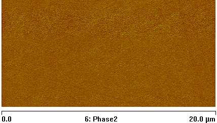
2 and subsurface images of a sample can be obtained from SPAM in situ simultaneously, the local elastic/electric/magnetic/thermal properties can also be obtained with different type of probes. There are three operation modes of SPAM: Sample Vibration Mode (SVM, i.e. contact mode) 4-6, Probe Vibration Mode (PVM, i.e. intermittent contact mode) 7-18, and resonant difference-frequency mode 16. In this paper, we set up a SPAM system by adding an acoustic module to a Dimension 3100 SPM system (Veeco Inc.) and operate in the first two modes. The thicknesses of HfO 2 film and SiO 2 substrate are ± 0.10 nm and 1.50 ± 0.01 mm respectively. The probe type is AppNano Sicon-200, the probe s resonant frequency is f 0 = 5-25 khz, the elastic constant is k = N/m, the relative humidity is %, and the temperature is Surface and subsurface topographies 2.1 Surface topography Topography shows that the HfO 2 film s surface is relatively smooth. The roughness is less than 2.61 ± 0.01 nm. 0 nm 500 nm
 shows some random lines on the subsurface of the sample while surface topography has not.")
3 Fig.1 Topography of a nano HfO 2 film on SiO 2 substrate 2.2 Subsurface topography Acoustic phase image of Sample Vibration Mode (SVM) shows some random lines on the subsurface of the sample while surface topography has not. Reviewing the whole coating procedure, we believe these lines should come from substrate surface scratching during the polishing procedure. As shown in Fig. 2, the width of a scratch is measured as µm, which is consistent with nm radius of abrasive. The acoustic frequency of sample vibration is f SV = 45 khz. 0 30
4 Width = µm Section Fig.2 Subsurface topography with some random lines. The detection of the subsurface structural and mechanical properties of a material is an advantage of the SPAM. One feature of the SPAM is the detection depth is very sensitive to the frequency. The lower the frequency, the deeper the detection depth. For this sample and this probe (f 0 = khz, k = N/m), 45 khz is the best frequency to detect the depth of film as shown in Fig. 3.


5 0 30 a) 24.6 khz b) 35.2 khz
")
 88.")
6 c) 35.8 khz d) 45.0 khz e) 88.2 khz
 of the biggest resonant peak is the best frequency to detect the depth of film 3.")
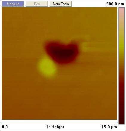
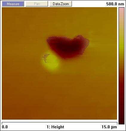
7 f) khz g) System frequency sweep Fig.3 Scratches in different acoustic phase images with different frequencies. The frequency (45 khz) of the biggest resonant peak is the best frequency to detect the depth of film 3. Laser-damaged nano-film To detect the damage threshold of the film, the sample was irradiated for 10 ns by an 1064 nm laser of 1/e 2 mm radius, 10 J/cm 2 power. During the high power laser's irradiation, HfO 2 film absorbs the heat, which leads to thermal and stress gradient and might even melt and be damaged locally when laser power exceeds the damage threshold. Except for damaged hole, the residual thermal stress might occur, the porosity and porous structure might change in the film damaged area leading to the change of film s hydrophilicity. 3.1 Depth of laser - damaged hole There are some laser-damaged holes appeared on the surface of the film. As shown in Fig. 4, the hole is irregular circular and the vertical depth of the hole was ± 0.10 nm, a little smaller than the thickness of the film ± 0.10 nm. We also find the width of scratches is somewhere between nm.
8 Depth = nm 0 nm 500 nm a) b) Width = µm 0 mv 160 mv c) d) Fig. 4 a) Topography of laser-damaged hole; b) Section of the hole along the white line in a) with nm depth close to the film thickness; c) Amplitude image of acoustic signal shows the scratches underneath the film; and d) Width of the scratches is around nm. 3.2 Residual stress The phase image of acoustic signal from another hole shows there is residual thermal stress around the laser-damaged hole. The average acoustic phase of this area is about 20 degrees higher than other area.
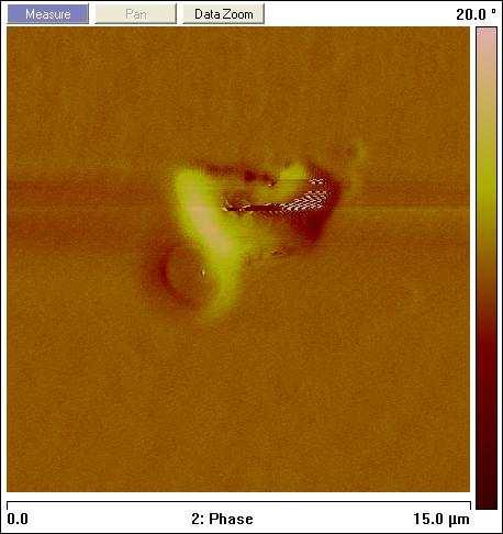
9 Fig. 5 residual thermal stress around damaged area 3.3 Hydrophilicity When the laser irradiation power exceeds the film s damage threshold, local porosity and porous structure might change in the film s damaged area which leads to the change of film s hydrophilicity. The sample in Fig. 6 was ongoing exposed to the air during the experiment. It is imaged with the PVM which is sensitive to water layer absorbed on the sample surface. The damping force of water layer will produce another vibration of the probe additional to the resonant vibration, which has greater effect on phase image of PVM than on height image. Fig. 6a) and b) were pictures of the sample when it is just taken out from the sealed bag. Fig. 6c) and d) were pictures 15 minutes afterwards, and Fig. 6e) and f) another 15 minutes later. Fig. 6a), c) and e) are height images, the others are phase images. Fig. 6g) is the section of 6f). The phase images show clearly that the film s damaged area and one side of splatter spot absorbed increasing amount of water from the air with the time exposed to the air while the undamaged area of film was hardly changed. The working frequency of this tip-sample system in PVM is f PV = 240 khz, while relative humidity is 45%. 0 nm 500 nm 0 20
 e) f)")


10 a) b) c) d) e) f) g)
11 Fig. 6 The phase images of PVM shows that the absorption to water vapor in air in the damaged area of HfO 2 film was stronger than in the undamaged area. f PV = 240 khz. 4. Conclusion Quantitative and qualitative results of structural and mechanical properties of a nano HfO 2 film on SiO 2 substrate using SPAM are presented in this paper. Surface topographies show that the roughness of film surface is less than 3 nm, while a lot of scratches due to polishing are observed on the SiO 2 substrate s surface under the HfO 2 film with SVM. After high power laser irradiation, damaged holes with depth close to the thickness of film appear in the film. Residual stress due to heat absorbing is observed within film with SVM. The phase images in PVM show that the hydrophilicity of the damaged area on the HfO 2 film is higher than the undamaged area, which leads to stronger absorption of water vapor in the air. We also find that the detection depth of SVM is sensitive to the sample vibration frequency, which means appropriate frequency should be chosen for detecting scratches and residual stress underneath or in a nano film. In conclusion, SPAM can be used as a quantitative and qualitative evaluation tools for subsurface damage of optical film. It will help better fabrication and usage of optical film. Acknowledgements This work was supported by the National Natural Science Foundation of China (No ). References 1. A. Callegari, E. Cartier, M. Gribelyuk, et al., 'Physical and electrical characterization of hafnium oxide and hafnium silicate sputtered films', J. Appl. Phys., Vol. 90, No. 12, pp , J.D.T. Kruschwitz and W.T. Pawlewicz, et al., 'Optical and durability properties of infrared transmitting thin films', Appl. Opt., Vol. 36, No. 10, pp , M. Alvisi, F. De Tomasi, M.R. Perronea, et al., 'Laser damage dependence on structural and optical properties of ion-assisted HfO2 thin films', Thin Solid Films, Vol. 396, No. 1-2, pp , H.R. Zeng, H.F. Yu, L.N. Zhang, et al., 'Local elastic response of individual grains in lead free Nb doped Bi4Ti3O12 piezoelectric ceramics', physica status solidi (a), Vol. 202, pp. R41 R43, Feb 2005.
12 5. O.V. Kolosov, M.R. Castell, C.D. Marsh, and G.D. Briggs, ' Imaging the elastic nanostructure of Ge islands by ultrasonic force microscopy', Phys. Rev. Letts, Vol. 81, No.5, , E. Kester, U. Rabe, L. Presmanes, Ph. Tailhades, and W. Arnold, ' Measurement of mechanical properties of nanoscaled ferrites using atomic force microscopy at ultrasonic frequencies', NanoStructured Materials, Vol. 12, No. 5-8, pp , Y.J. Zhao, Q. Cheng, M.L. Qian and J.H. Cantrell, 'Phase image contrast mechanism in intermittent contact atomic force microscopy', J. Appl. Phys. Vol. 108, pp , Nov Y.J. Zhao, Q. Cheng and M.L. Qian, 'Frequency Response of the Sample Vibration Mode in Scanning Probe Acoustic Microscope', Chin. Phys. Lett., Vol. 27, No. 5, pp , May P. Thota, S. MacLaren, and H. Dankowicz, 'Controlling bistability in tapping-mode atomic force microscopy using dual-frequency excitation', Appl. Phys. Lett., Vol. 91, No. 9, pp , Aug S. Basak and A. Raman, 'Dynamics of tapping mode atomic force microscopy in liquids: Theory and experiments', Appl. Phys. Lett., Vol. 91, No. 6, pp , Jun Y. Lin, X. C. Shen, J. J. Wang, et al., 'Measuring radial Young's modulus of DNA by tapping mode AFM', Chin. Sci. Bull., Vol. 52, No. 23, pp , Dec D. Solares, 'Eliminating bistability and reducing sample damage through frequency and amplitude modulation in tapping-mode atomic force microscopy', Meas. Sci. Technol., Vol. 18, pp , Jan A. Raman, J. Melcher, and R. Tung, 'Cantilever dynamics in atomic force microscopy', Nanotoday, Vol. 3, No. 1-2, pp , Feb W. Xu, M. Wood-Adams, and C.G. Robertson, ' Measuring local viscoelastic properties of complex materials with tapping mode atomic force microscopy', Polymer, Vol. 47, No. 13, pp , Jun T. Fukuma, J.I. Kilpatrick, and S.P. Jarvis, ' Phase modulation atomic force microscope with true atomic resolution', Rev. Sci. Instrum., Vol. 77, No. 12, pp , S.A. Cantrell, J.H. Cantrell, and P.T. Lillehei, 'Nanoscale subsurface imaging via resonant difference-frequency atomic force ultrasonic microscopy', J. Appl. Phys. No. 101, No. 11, pp , Jun Y. Song and B. Bhushan, 'Simulation of dynamic modes of atomic force microscopy using a 3D finite element model', Ultramicroscopy, Vol. 106, No. 8-9, pp , Jul 2006.
13 18. J. Polesel-Maris and S. Ganthier, ' A virtual dynamic atomic force microscope for image calculations', J. Appl. Phys., Vol. 97, No. 4, pp , Feb Wengang Yao, Qian Cheng, 'The Detection of Different Physical Properties of Laser-Damaged HfO2 Film on Sio2 Substrate by Scanning Probe Acoustic Microscope', Advanced Materials Research, Vol , pp , 2001.
PROCEEDINGS OF SPIE. Thin-film polarizer for high power laser system in China
 PROCEEDINGS OF SPIE SPIEDigitalLibrary.org/conference-proceedings-of-spie Thin-film polarizer for high power laser system in China Jianda Shao, Kui Yi, Meiping Zhu Jianda Shao, Kui Yi, Meiping Zhu, "Thin-film
CHAPTER 9 AFM PROFILING AND NANOLITHOGRAPHY WITH NEEDLE-TIPPED CANTILEVERS
 CHAPTER 9 AFM PROFILING AND NANOLITHOGRAPHY WITH NEEDLE-TIPPED CANTILEVERS Since Ag 2 Ga nanoneedles can be directly grown on (or even in place of) the tips on AFM cantilevers using the pulling technique
Local Oxide Growth Mechanisms on Nickel Films
 Materials Transactions, Vol. 48, No. 3 (2007) pp. 471 to 475 #2007 The Japan Institute of Metals Local Oxide Growth Mechanisms on Nickel Films Te-Hua Fang* 1 and Kuan-Jen Chen* 2 Institute of Mechanical
Magnetic Force Microscopy: nanoscale magnetic imaging and lithography
 NTEGRA Aura Magnetic Force Microscopy: nanoscale magnetic imaging and lithography The principle of Magnetic Force Microscopy (MFM) is based on the detection of the interaction between the sample and a
Evaluation of Mechanical Properties of Hard Coatings
 Evaluation of Mechanical Properties of Hard Coatings Comprehensive mechanical testing of two coated metal samples was performed on the UNMT- 1. The tests clearly distinguished brittle and ductile samples,
Laser damage threshold of AR coatings on phosphate glass
 Laser damage threshold of AR coatings on phosphate glass Optical Coatings for Laser Applications Wednesday, 12 th April 2017, Buchs SG, Switzerland dirk.apitz@schott.com, SCHOTT Suisse SA, Advanced Optics,
Fabrication and application of high quality diamond coated. CMP pad conditioners
 Fabrication and application of high quality diamond coated CMP pad conditioners Hua Wang 1,a, Fanghong Sun 1,b* 1 School of Mechanical Engineering, Shanghai Jiao Tong University, Shanghai, 200240, China
Advanced Manufacturing Choices
 Advanced Manufacturing Choices Table of Content Mechanical Removing Techniques Ultrasonic Machining (USM) Sputtering and Focused Ion Beam Milling (FIB) Ultrasonic Machining In ultrasonic machining (USM),
Fabrication of Micro and Nano Structures in Glass using Ultrafast Lasers
 Fabrication of Micro and Nano Structures in Glass using Ultrafast Lasers Denise M. Krol University of California, Davis IMI Glass Workshop Washington DC April 15-17, 2007 Femtosecond laser modification
Title: Localized surface plasmon resonance of metal nanodot and nanowire arrays studied by far-field and near-field optical microscopy
 Contract Number: AOARD-06-4074 Principal Investigator: Heh-Nan Lin Address: Department of Materials Science and Engineering, National Tsing Hua University, 101, Sec. 2, Kuang Fu Rd., Hsinchu 30013, Taiwan
Application Note #124 VITA: Quantitative Nanoscale Characterization and Unambiguous Material Identification for Polymers
 Local thermal analysis identifies polymer AFM image of polymer blend Application Note #124 VITA: Quantitative Nanoscale Characterization and Unambiguous Material Identification for Polymers VITA module
Scanning thermal microscopy probe capable of simultaneous electrical imaging and the addition of a diamond tip
 Scanning thermal microscopy probe capable of simultaneous electrical imaging and the addition of a diamond tip E Brown, L Hao, D C Cox and J C Gallop National Physical Laboratory, Hampton Road, Teddington,
Fabrication of micro/nano structures in glass by lasers
 Lehigh University Lehigh Preserve International Workshop on Scientific Challenges for Glass Research Glass Conferences and Workshops Spring 4-1-2007 Fabrication of micro/nano structures in glass by lasers
Influence of plasma treatment on laser-induced damage characters of HfO 2 thin films at 355nm
 Influence of plasma treatment on laser-induced damage characters of HfO 2 thin films at 355nm Dongping Zhang 1,*, Congjuan Wang 2, Ping Fan 1, Xingmin Cai 1, Zhuanghao Zheng 1, Jianda Shao 2, and Zhengxiu
nano-ta TM : Nano Thermal Analysis
 nano-ta TM : Nano Thermal Analysis Application Note #10 Correlation between nanoscale and bulk Thermal Analysis Authors: Dr. Greg Meyers and Dr. Andrew Pastzor Dow Chemical Introduction Thermal methods
Prometheus-L Reactor Building Layout
 Prometheus-L Reactor Building Layout Two Main Options for the Final Optic (1) SiO 2 or CaF 2 wedges 85 40 cm stiff, lightweight, actively cooled, neutron transparent substrate 4.6 m (2) Grazing incidence
Tribological and Mechanical Characterization of Carbon-Coated Sliders and Disks
 Tribol Lett (21) :23 29 DOI 1.17/s1129-9-92-1 ORIGINAL PAPER Tribological and Mechanical Characterization of Carbon-Coated Sliders and Disks R. Brunner F. E. Talke Received: 27 July 29 / Accepted: 2 September
Imaging of Microstructural Features and Local Stiffness of α and β Phases in Titanium Ti-6Al-4V Alloy by Atomic Force Acoustic Microscopy
 5th International Workshop NDT in Progress Meeting of NDT experts, October 12 14, 2009 Prague, Czech Republic, Hotel and Congress center Floret Imaging of Microstructural Features and Local Stiffness of
Identifying Cohesive Failure of Screen Protectors with Acoustic Emission
 Identifying Cohesive Failure of Screen Protectors with Acoustic Emission Prepared by Frank Liu 6 Morgan, Ste156, Irvine CA 92618 P: 949.461.9292 F: 949.461.9232 nanovea.com Today's standard for tomorrow's
Preparation and characterization of Co BaTiO 3 nano-composite films by the pulsed laser deposition
 Journal of Crystal Growth 289 (26) 48 413 www.elsevier.com/locate/jcrysgro Preparation and characterization of Co BaTiO 3 nano-composite films by the pulsed laser deposition Wu Weidong a,b,, He Yingjie
Organisation and melting of solution grown truncated lozenge polyethylene single crystals
 e-polymers 2003, no. 051. http://www.e-polymers.org ISSN 1618-7229 Organisation and melting of solution grown truncated lozenge polyethylene single crystals Mingwen Tian 1,2, Joachim Loos 1 * 1 Department
Surface Characterization with Nanometer Lateral Resolution Using the Vibration Modes of Atomic Force Microscope Cantilevers
 ECNDT 2006 - We.2.2.3 Surface Characterization with Nanometer Lateral Resolution Using the Vibration Modes of Atomic Force Microscope Cantilevers Ute RABE, Arnaud CARON, Kerstin SCHWARZ, Sigrun HIRSEKORN,
Integrated Silicon Heater for Tip-Based. Nanomanufacturing
 Supporting Information Wear Resistant Diamond Nanoprobe Tips with Integrated Silicon Heater for Tip-Based Nanomanufacturing Patrick C. Fletcher 1, Jonathan R. Felts 1, Zhenting Dai 1, Tevis T.B. Jacobs
Deposited by Sputtering of Sn and SnO 2
 Journal of the Korean Ceramic Society Vol. 49, No. 5, pp. 448~453, 2012. http://dx.doi.org/10.4191/kcers.2012.49.5.448 Comparative Study of Nitrogen Incorporated SnO 2 Deposited by Sputtering of Sn and
Enhanced Light Trapping in Periodic Aluminum Nanorod Arrays as Cavity Resonator
 Enhanced Light Trapping in Periodic Aluminum Nanorod Arrays as Cavity Resonator Rosure B. Abdulrahman, Arif S. Alagoz, Tansel Karabacak Department of Applied Science, University of Arkansas at Little Rock,
Nanoscratch evaluation of adhesive strength of Cu/PI films
 Computer Methods and Experimental Measurements VIII 303 Nanoscratch evaluation of adhesive strength of Cu/PI films K. Tanaka, K. Gunji & T. Katayama Department of Mechanical Engineering, Doshisha University,
Ceramic Processing Research
 Journal of Ceramic Processing Research. Vol. 11, No. 1, pp. 100~106 (2010) J O U R N A L O F Ceramic Processing Research Factors affecting surface roughness of Al 2 O 3 films deposited on Cu substrates
Spatter-Free Stable Conduction and Keyhole Welding of Copper with 275 Watt Blue Laser
 Spatter-Free Stable Conduction and Keyhole Welding of Copper with 275 Watt Blue Laser Abstract Laser welding of highly reflective materials such as copper has been problematic for infrared lasers due to
ZnO-based Transparent Conductive Oxide Thin Films
 IEEE EDS Mini-colloquium WIMNACT 32 ZnO-based Transparent Conductive Oxide Thin Films Weijie SONG Ningbo Institute of Material Technology and Engineering, Chinese Academy of Sciences, Ningbo, P. R. China
Integration of an optical fiber taper with an optical. microresonator fabricated in glass by femtosecond laser 3D. micromachining
 Integration of an optical fiber taper with an optical microresonator fabricated in glass by femtosecond laser 3D micromachining Jiangxin Song a,b, Jintian Lin a,b, Jialei Tang a,b, Lingling Qiao a, Ya
Microstructure, morphology and their annealing behaviors of alumina films synthesized by ion beam assisted deposition
 Nuclear Instruments and Methods in Physics Research B 206 (2003) 357 361 www.elsevier.com/locate/nimb Microstructure, morphology and their annealing behaviors of alumina films synthesized by ion beam assisted
EARLY STAGES OF THE CHEMICAL VAPOR DEPOSITION OF PYROLYTIC CARBON INVESTIGATED BY ATOMIC FORCE MICROSCOPY
 EARLY STAGES OF THE CHEMICAL VAPOR DEPOSITION OF PYROLYTIC CARBON INVESTIGATED BY ATOMIC FORCE MICROSCOPY Andreas Pfrang 1, Yong-Zhong Wan 1, Virginie De Pauw 2,WinfriedSend 2,Dagmar Gerthsen 2, Thomas
BLOCK COPOLYMERS ORGANIZATION AT INTERFACE
 THE 19 TH INTERNATIONAL CONFERENCE ON COMPOSITE MATERIALS BLOCK COPOLYMERS ORGANIZATION AT INTERFACE D.Fischer, S. Bistac *, M. Brogly, Université de Haute Alsace, LPIM, Mulhouse France * Corresponding
PeakForce Tapping and ScanAsyst An introduction to the technique featuring Bruker s Dimension Edge. Bede Pittenger, Ph.D.
 PeakForce Tapping and ScanAsyst An introduction to the technique featuring Bruker s Dimension Edge Bede Pittenger, Ph.D. Dimension Edge with ScanAsyst: High performance AFM breaking down cost and productivity
Damage Threats and Response of Final Optics for Laser-Fusion Power Plants
 Damage Threats and Response of Final Optics for Laser-Fusion Power Plants M. S. Tillack 1, S. A. Payne 2, N. M. Ghoniem 3, M. R. Zaghloul 1 and J. F. Latkowski 2 1 UC San Diego, La Jolla, CA 92093-0417
CONTENTS. Introduction. NSOM Optical Fiber Probes
 CONTENTS Introduction NSOM Optical Fiber Probes AFM Probes AFM Probes Hard to achieve Force Constants and Resonance Frequencies Deep Trench AFM Probes Electrical and STM Probes Hollow AFM Nanopipette Probes
NanoTA2 Sub-100nm Local Thermal Imaging and Analysis
 Anasys Instruments introduces the second generation of its award winning nano thermal analysis product, the NanoTA2. This system extends the capabilities of the nano-ta system by the addition of local
Interface Structure and Charge Trapping in HfO 2 -based MOSFETS
 Interface Structure and Charge Trapping in HfO 2 -based MOSFETS MURI - ANNUAL REVIEW, 13 and 14 th May 2008 S.K. Dixit 1, 2, T. Feng 6 X.J. Zhou 3, R.D. Schrimpf 3, D.M. Fleetwood 3,4, S.T. Pantelides
PATTERNING OF OXIDE THIN FILMS BY UV-LASER ABLATION
 Journal of Optoelectronics and Advanced Materials Vol. 7, No. 3, June 2005, p. 1191-1195 Invited lecture PATTERNING OF OXIDE THIN FILMS BY UV-LASER ABLATION J. Ihlemann * Laser-Laboratorium Göttingen e.v.,
Silver Diffusion Bonding and Layer Transfer of Lithium Niobate to Silicon
 Chapter 5 Silver Diffusion Bonding and Layer Transfer of Lithium Niobate to Silicon 5.1 Introduction In this chapter, we discuss a method of metallic bonding between two deposited silver layers. A diffusion
Repetition: Adhesion Mechanisms
 Repetition: Adhesion Mechanisms a) Mechanical interlocking b) Monolayer/monolayer c) Chemical bonding d) Diffusion e) Psedo diffusion due to augmented energy input (hyperthermal particles) Repetition:
Structure of mixed-phase Si films studied by C- AFM and X-TEM
 Journal of Physics: Conference Series Structure of mixed-phase Si films studied by C- AFM and X-TEM To cite this article: T Mates et al 2007 J. Phys.: Conf. Ser. 61 790 Related content - Making the most
Using Atomic Force Microscopy (AFM) for Engineering Low Scatter Thin Film Optics
 for Engineering Low Scatter Thin Film Optics") The World Leader In Scanning Probe Microscopy Using Atomic Force Microscopy (AFM) for Engineering Low Scatter Thin Film Optics By A. Duparré, N. Kaiser, M.G. Heaton Figure 2: AFM image of the surface structures
The World Leader In Scanning Probe Microscopy Using Atomic Force Microscopy (AFM) for Engineering Low Scatter Thin Film Optics By A. Duparré, N. Kaiser, M.G. Heaton Figure 2: AFM image of the surface structures
Preparation and structural characterization of thin-film CdTe/CdS heterojunctions
 JOURNAL OF OPTOELECTRONICS AND ADVANCED MATERIALS Vol. 8, No., June 006, p. 96-940 Preparation and structural characterization of thin-film CdTe/ heterojunctions I. SALAORU a, P. A. BUFFAT b, D. LAUB b,
PbS NANO THIN FILM PHOTOCONDUCTIVE DETECTOR
 International Journal of Physics and Research (IJPR) ISSN 2250-0030 Vol. 3, Issue 3, Aug 2013, 21-26 TJPRC Pvt. Ltd. PbS NANO THIN FILM PHOTOCONDUCTIVE DETECTOR SUDAD S. AHMED, EMAN K. HASSAN & FATN EMAD
Co-Evolution of Stress and Structure During Growth of Polycrystalline Thin Films
 Co-Evolution of Stress and Structure During Growth of Polycrystalline Thin Films Carl V. Thompson and Hang Z. Yu* Dept. of Materials Science and Engineering MIT, Cambridge, MA, USA Effects of intrinsic
Tennessee State University College of Engineering and Technology Department of Mechanical Engineering
 Tennessee State University College of Engineering and Technology Department of Mechanical Engineering The Impact of Modeling, Simulation, and Characterization of the Mechanical Properties of Nano-materials
In the Proceedings of the Second Asia-Pacific Workshop on Near-field Optics, Beijing, China, October 20-23, 1999.
 In the Proceedings of the Second Asia-Pacific Workshop on Near-field Optics, Beijing, China, October 20-23, 1999. NEAR-FIELD SCANNING OPTICAL MICROSCOPY OF ELECTROMIGRATION IN YBCO Suzanne Huerth, Michael
Detection of Skin Disbond in Honeycombs and Coating Detachment by Laser Tapping Technique
 1st International Symposium on Laser Ultrasonics: Science, Technology and Applications July 16-18 2008, Montreal, Canada Detection of Skin Disbond in Honeycombs and Coating Detachment by Laser Tapping
Effects of substrate temperature and ambient oxygen pressure on growth of Ba(Fe 1/2 Nb 1/2 )O 3 thin films by pulsed laser deposition
O 3 thin films by pulsed laser deposition") Article Materials Science September 2013 Vol.58 No.27: 3398 3402 doi: 10.1007/s11434-013-5980-2 Effects of substrate temperature and ambient oxygen pressure on growth of Ba(Fe 1/2 Nb 1/2 )O 3 thin films
Article Materials Science September 2013 Vol.58 No.27: 3398 3402 doi: 10.1007/s11434-013-5980-2 Effects of substrate temperature and ambient oxygen pressure on growth of Ba(Fe 1/2 Nb 1/2 )O 3 thin films
Supplimentary Information. Large-Scale Synthesis and Functionalization of Hexagonal Boron Nitride. Nanosheets
 Electronic Supplementary Material (ESI) for Nanoscale. This journal is The Royal Society of Chemistry 2014 Supplimentary Information Large-Scale Synthesis and Functionalization of Hexagonal Boron Nitride
Optical Coatings. Photonics 4 Luxury Coatings , Genève. Dr. Andreas Bächli Head of Optical Coatings at RhySearch, Buchs (SG)
") Optical Coatings Photonics 4 Luxury Coatings 21.06.2017, Genève Dr. Andreas Bächli Head of Optical Coatings at RhySearch, Buchs (SG) RhySearch The Research- and Innovation Center in the Rhine Valley RhySearch
Optical Coatings Photonics 4 Luxury Coatings 21.06.2017, Genève Dr. Andreas Bächli Head of Optical Coatings at RhySearch, Buchs (SG) RhySearch The Research- and Innovation Center in the Rhine Valley RhySearch
Interface quality and thermal stability of laser-deposited metal MgO multilayers
 Interface quality and thermal stability of laser-deposited metal MgO multilayers Christian Fuhse, Hans-Ulrich Krebs, Satish Vitta, and Göran A. Johansson Metal MgO multilayers metal of Fe, Ni 80 Nb 20,
Excimer Laser Annealing of Hydrogen Modulation Doped a-si Film
 Materials Transactions, Vol. 48, No. 5 (27) pp. 975 to 979 #27 The Japan Institute of Metals Excimer Laser Annealing of Hydrogen Modulation Doped a-si Film Akira Heya 1, Naoto Matsuo 1, Tadashi Serikawa
Tribomechanical Properties of DLC Coatings Deposited by Magnetron Sputtering on Metallic and Insulating Substrates
 Tribomechanical Properties of DLC Coatings Deposited by Magnetron Sputtering on Metallic and Insulating Substrates Dr. Iván Fernández Martínez Indianapolis, May 10th, 2016 Diamond Like Carbon (DLC) Diamond-like
scattering study of phase separation at initially mixed HfO 2 -SiO
 ERC TeleSeminar In situ low-angle x-ray x scattering study of phase separation at initially mixed HfO -SiO thin film interfaces Paul C. McIntyre Jeong-hee Ha Department of Materials Science and Engineering,
Surface Modification of Cr-Mo Steel Using New Water Jet Cavitation Technology
 Research & Reviews: Journal of Material Science DOI: 10.4172/2321-6212.1000209 e-issn: 2321-6212 www.rroij.com Surface Modification of Cr-Mo Steel Using New Water Jet Cavitation Technology Masataka Ijiri
The Effect of Annealing Heat Treatment on Structural and Optical Properties of Ce-doped ZnO Thin Films
 4th International Conference on Computer, Mechatronics, Control and Electronic Engineering (ICCMCEE 2015) The Effect of Annealing Heat Treatment on Structural and Optical Properties of Ce-doped Thin Films
LOW TEMPERATURE GROWTH OF SMOOTH INDIUM TIN OXIDE FILMS BY ULTRAVIOLET ASSISTED PULSED LASER DEPOSITION
 Journal of Optoelectronics and Advanced Materials Vol. 4, No. 1, March 2002, p. 21-25 LOW TEMPERATURE GROWTH OF SMOOTH INDIUM TIN OXIDE FILMS BY ULTRAVIOLET ASSISTED PULSED LASER DEPOSITION V. Craciun,
ARTICLE IN PRESS. Materials Science in Semiconductor Processing
 Materials Science in Semiconductor Processing ] (]]]]) ]]] ]]] Contents lists available at ScienceDirect Materials Science in Semiconductor Processing journal homepage: www.elsevier.com/locate/mssp High-dielectric
Characterization of Materials with a Combined AFM/Raman Microscope
 Characterization of Materials with a Combined AFM/Raman Microscope Marko Surtchev 1, Sergei Magonov 1 and Mark Wall 2 1 NT-MDT America, Tempe, AZ U.S.A. 2 Thermo Fisher Scientific, Madison, WI, U.S.A.
Integrative In-situ Detection of Defects in Aeroengine Blades Combining Borescope and Eddy Current Techniques
 18th World Conference on Nondestructive Testing, 16-20 April 2012, Durban, South Africa Integrative In-situ Detection of Defects in Aeroengine Blades Combining Borescope and Eddy Current Techniques Wugang
Nanomechanical Properties of Biologically Significant Microstructural Elements of Wood
 Nanomechanical Properties of Biologically Significant Microstructural Elements of Wood Valery Bliznyuk, Roman Rabiej, Ondrej Pekarovic Western Michigan University, Kalamazoo, MI 49008 Objectives To reveal
Magnetic patterning: local manipulation of the intergranular. exchange coupling via grain boundary engineering
 Magnetic patterning: local manipulation of the intergranular exchange coupling via grain boundary engineering Kuo-Feng Huang, 1 Jung-Wei Liao, 1 Cheng-Yu Hsieh, 2 Liang-Wei Wang, 1 Yen-Chun Huang, 1 Wei-Chih
DEPOSITION OF Al 2 O 3 ON CERAMIC SUBSTRATES BY PECVD METHOD. Lucie Špirková a Vlastimil Brožek a Jean Durand b
 DEPOSITION OF Al 2 O 3 ON CERAMIC SUBSTRATES BY PECVD METHOD Lucie Špirková a Vlastimil Brožek a Jean Durand b a) Institute of Chemical Technology, 166 28 Prague, Czech Republic b) Laboratoire des Matériaux
micromachines ISSN X
 Micromachines 2012, 3, 55-61; doi:10.3390/mi3010055 Article OPEN ACCESS micromachines ISSN 2072-666X www.mdpi.com/journal/micromachines Surface Plasmon Excitation and Localization by Metal-Coated Axicon
Grain Sizes and Surface Roughness in Platinum and Gold Thin Films. L.L. Melo, A. R. Vaz, M.C. Salvadori, M. Cattani
 Journal of Metastable and Nanocrystalline Materials Vols. 20-21 (2004) pp. 623-628 online at http://www.scientific.net 2004 Trans Tech Publications, Switzerland Grain Sizes and Surface Roughness in Platinum
Morphology of Thin Aluminum Film Grown by DC Magnetron Sputtering onto SiO 2 on Si(100) Substrate
 Substrate") Morphology of Thin Aluminum Film Grown by DC Magnetron Sputtering onto SiO 2 on Si(1) Substrate Fan Wu Microelectronics Center, Medtronic Inc., Tempe, AZ 85261 James E. Morris Department of Electrical
Morphology of Thin Aluminum Film Grown by DC Magnetron Sputtering onto SiO 2 on Si(1) Substrate Fan Wu Microelectronics Center, Medtronic Inc., Tempe, AZ 85261 James E. Morris Department of Electrical
NEBRASKA NANOSCALE FACILITY CHARACTERIZATION FACILITIES
 NEBRASKA NANOSCALE FACILITY CHARACTERIZATION FACILITIES Jeff Shield Department of Mechanical & Materials Engineering Nebraska Center for Materials and Nanoscience National Nanotechnology Coordinated Infrastructure
Micro-Electro-Mechanical Systems (MEMS) Fabrication. Special Process Modules for MEMS. Principle of Sensing and Actuation
 Fabrication. Special Process Modules for MEMS. Principle of Sensing and Actuation") Micro-Electro-Mechanical Systems (MEMS) Fabrication Fabrication Considerations Stress-Strain, Thin-film Stress, Stiction Special Process Modules for MEMS Bonding, Cavity Sealing, Deep RIE, Spatial forming
Micro-Electro-Mechanical Systems (MEMS) Fabrication Fabrication Considerations Stress-Strain, Thin-film Stress, Stiction Special Process Modules for MEMS Bonding, Cavity Sealing, Deep RIE, Spatial forming
Chapter 3: Powders Production and Characterization
 Chapter 3: Powders Production and Characterization Course Objective... To introduce selective powder production processes and characterization methods. This course will help you : To understand properties
HONEYCOMB MECHANICAL BEHAVIOR USING MACROINDENTATION
 HONEYCOMB MECHANICAL BEHAVIOR USING MACROINDENTATION. Prepared by Duanjie Li, PhD 6 Morgan, Ste156, Irvine CA 92618 P: 949.461.9292 F: 949.461.9232 nanovea.com Today's standard for tomorrow's materials.
Supporting Information
 Supporting Information Thermal Oxidation of WSe 2 Nano-sheets Adhered on SiO 2 /Si Substrates Yingnan Liu, a, Cheng Tan, b,c, Harry Chou, c Avinash Nayak, b Di Wu, a Rudresh Ghosh, c Hsiao- Yu Chang, b
Full Nanomechanical Characterization of Ultra-Thin Films
 APPLICATION NOTE By: Jeffrey Schirer and Julia Nowak, Ph.D. Hysitron, Inc. Eiji Kusano and Mune-aki Sakamoto Department of Chemistry, Kanazawa Institute of Technology, Japan Full Nanomechanical Characterization
EFFECT OF GROWTH TEMPERATURE ON THE CATALYST-FREE GROWTH OF LONG SILICON NANOWIRES USING RADIO FREQUENCY MAGNETRON SPUTTERING
 International Journal of Nanoscience Vol. 10, Nos. 1 & 2 (2011) 13 17 #.c World Scienti c Publishing Company DOI: 10.1142/S0219581X11007594 EFFECT OF GROWTH TEMPERATURE ON THE CATALYST-FREE GROWTH OF LONG
Supplementary Information
 Supplementary Information Supplementary Figure 1 Characterization of precursor coated on salt template. (a) SEM image of Mo precursor coated on NaCl. Scale bar, 50 μm. (b) EDS of Mo precursor coated on
An XPS and Atomic Force Microscopy Study of the Micro-Wetting Behavior of Water on Pure Chromium* 1
 Materials Transactions, Vol. 44, No. 3 (2003) pp. 389 to 395 #2003 The Japan Institute of Metals An XPS and Atomic Force Microscopy Study of the Micro-Wetting Behavior of Water on Pure Chromium* 1 Rongguang
Effect of Substrate Discontinuities on the Propagating Surface Plasmon Polariton
 Electronic Supplementary Material (ESI) for Nanoscale. This journal is The Royal Society of Chemistry 2014 Supplemental Information for: Effect of Substrate Discontinuities on the Propagating Surface Plasmon
Weight (%) Temperature ( C)
 Temperature ( C)") Weight (%) 100 80 60 40 20 0 0 100 200 300 400 500 600 Temperature ( C) Supplementary Figure 1. Thermal analysis of (UPyU) 3 TMP. Thermogravimetric analysis (TGA) curve of (UPyU) 3 TMP from 25 to 600 C.
Weight (%) 100 80 60 40 20 0 0 100 200 300 400 500 600 Temperature ( C) Supplementary Figure 1. Thermal analysis of (UPyU) 3 TMP. Thermogravimetric analysis (TGA) curve of (UPyU) 3 TMP from 25 to 600 C.
EDGE CHIPPING RESISTANCE USING MACROINDENTATION TESTING
 EDGE CHIPPING RESISTANCE USING MACROINDENTATION TESTING Prepared by Ali Mansouri 6 Morgan, Ste156, Irvine CA 92618 P: 949.461.9292 F: 949.461.9232 nanovea.com Today's standard for tomorrow's materials.
Progress in the Understanding of PEFC Degradation related to Liquid Water interactions
 Progress in the Understanding of PEFC Degradation related to Liquid Water interactions K. Andreas Friedrich, German Aerospace Center (DLR), Institute of Technical Thermodynamics Outline Introduction to
Surface Roughness Investigations on Nb Samples using Optical Profilometry
 Surface Roughness Investigations on Nb Samples using Optical Profilometry A. Navitski, S. Lagotzky, G. Müller FB C Physik, Bergische Universität Wuppertal gmueller@uni-wuppertal.de Motivation and strategy
SUPPLEMENTARY INFORMATION
 High Electrochemical Activity of the Oxide Phase in Model Ceria- and Ceria-Ni Composite Anodes William C. Chueh 1,, Yong Hao, WooChul Jung, Sossina M. Haile Materials Science, California Institute of Technology,
A Functional Micro-Solid Oxide Fuel Cell with. Nanometer Freestanding Electrolyte
 Electronic Supplementary Material (ESI) for Journal of Materials Chemistry A. This journal is The Royal Society of Chemistry 2017 SUPPLEMENTARY INFORMATION A Functional Micro-Solid Oxide Fuel Cell with
Techniques to Improve Coating Adhesion of Superhard Coatings
 Journal of Metals, Materials and Minerals. Vol.16 No.2 pp.19-23, 2006 Techniques to Improve Coating Adhesion of Superhard Coatings Nurot PANICH 1, Panyawat WANGYAO 1*, Nuntapol VATTANAPRATEEP 2 and Sun
Mechanical Properti es of ZnO:Mo Transparent Conducting Oxide Thin Film Prepared by Sputtering
 CHINESE JOURNAL OF PHYSICS VOL. 51, NO. 3 June 2013 Mechanical Properti es of ZnO:Mo Transparent Conducting Oxide Thin Film Prepared by Sputtering Y. C. Lin, C. C. Chen, and W. Y. Lai Department of Mechatronics
IMAGING OF MICROSTRUCTURAL FEATURES AND LOCAL STIFFNESS OF Α- AND Β-PHASES IN THE TITANIUM ALLOY TI- 6AL-4V BY ATOMIC FORCE ACOUSTIC MICROSCOPY
 IMAGING OF MICROSTRUCTURAL FEATURES AND LOCAL STIFFNESS OF Α- AND Β-PHASES IN THE TITANIUM ALLOY TI- 6AL-4V BY ATOMIC FORCE ACOUSTIC MICROSCOPY Jonas O. RABE, Ute RABE, Sigrun HIRSEKORN Fraunhofer Institute
Electronic Supplementary Information. Etching-free patterning method for electrical characterizations of atomically thin CVD-grown MoSe 2 film
 Electronic Supplementary Material (ESI) for Nanoscale. This journal is The Royal Society of Chemistry 2014 Electronic Supplementary Information Etching-free patterning method for electrical characterizations
Deposition of C-F Thin Films by Sputtering and Their Micromechanical Properties
 M. New Wang Diamond et al. and Frontier Carbon Technology 29 Vol. 15, No. 1 2005 MYU Tokyo NDFCT 472 Deposition of C-F Thin Films by Sputtering and Their Micromechanical Properties Mei Wang, Shuichi Watanabe
Heteroepitaxy of Monolayer MoS 2 and WS 2
 Supporting Information Seed Crystal Homogeneity Controls Lateral and Vertical Heteroepitaxy of Monolayer MoS 2 and WS 2 Youngdong Yoo, Zachary P. Degregorio, James E. Johns* Department of Chemistry, University
GURU JAMBHESHWAR, UNIVERSITY OF SCIENCE & TECHNOLOGY, HISAR Department of Bio & Nano Tech. GJUS&T, Hisar.
 GURU JAMBHESHWAR, UNIVERSITY OF SCIENCE & TECHNOLOGY, HISAR INVITATION FOR QUOTATION You are invited to submit your most competitive quotation for the following goods with item wise detailed specifications
MICRO-THERMAL, X-RAY AND RAMAN ANALYSES OF POLYOLEFIN INTERFACES
 MICRO-THERMAL, X-RAY AND RAMAN ANALYSES OF POLYOLEFIN INTERFACES T. Nishino, M. Kotera, D. Izumo, Y.Urushihara Graduate School of Engineering, Kobe University Rokko, Nada, Kobe 657-8501, Japan tnishino@kobe-u.ac.jp
Previous Lecture. Vacuum & Plasma systems for. Dry etching
 Previous Lecture Vacuum & Plasma systems for Dry etching Lecture 9: Evaporation & sputtering Objectives From this evaporation lecture you will learn: Evaporator system layout & parts Vapor pressure Crucible
A Study of the Formation Modes of Nanosized Oxide Structures of Gallium Arsenide by Local Anodic Oxidation
 ISSN 6-786, Semiconductors,, Vol. 6, No., pp. 66 6. Pleiades Publishing, Ltd.,. Original Russian Text O.A. Ageev, V.A. Smirnov, M.S. Solodovnik, A.V. Rukomoikin, V.I. Avilov,, published in Izvestiya vysshikh
Nano Wear Testing Polymer Coated Glass
 Nano Wear Testing Polymer Coated Glass Prepared by Jorge Ramirez 6 Morgan, Ste56, Irvine CA 9268 P: 949.46.9292 F: 949.46.9232 nanovea.com Today's standard for tomorrow's materials. 2 NANOVEA INTRO New
Vertical nano-composite heteroepitaxial thin films with manganites and ferroelectrics. Yonghang Pei Physics Department
 Vertical nano-composite heteroepitaxial thin films with manganites and ferroelectrics Yonghang Pei Physics Department Outline Introduction to MultiFerroics La 1 x Sr x MnO 3 Experiment Summary and Future
Supporting Information
 Copyright WILEY VCH Verlag GmbH & Co. KGaA, 69469 Weinheim, Germany, 2012. Supporting Information for Small, DOI: 10.1002/smll. 201102654 Large-Area Vapor-Phase Growth and Characterization of MoS 2 Atomic
Simple method for formation of nanometer scale holes in membranes. E. O. Lawrence Berkeley National Laboratory, Berkeley, CA 94720
 Simple method for formation of nanometer scale holes in membranes T. Schenkel 1, E. A. Stach, V. Radmilovic, S.-J. Park, and A. Persaud E. O. Lawrence Berkeley National Laboratory, Berkeley, CA 94720 When
Conductivity Mapping with Resolution of 140 nm in Diameter by Eddy Current Method Using Small Solenoid Coil
 Materials Transactions, Vol. 43, No. 12 (2002) pp. 3217 to 3221 c 2002 The Japan Institute of Metals Conductivity Mapping with Resolution of 140 nm in Diameter by Eddy Current Method Using Small Solenoid
Polycrystalline Silicon Produced by Joule-Heating Induced Crystallization
 Polycrystalline Silicon Produced by Joule-Heating Induced Crystallization So-Ra Park 1,2, Jae-Sang Ro 1 1 Department of Materials Science and Engineering, Hongik University, Seoul, 121-791, Korea 2 EnSilTech