Chin C. Lee Electrical Engineering & Computer Science Materials and Manufacturing Technology University of California, Irvine
|
|
|
- Lauren Lindsey
- 6 years ago
- Views:
Transcription
1 IEEE CPMT OC Chapter s Inaugural Technical meeting Sept. 20, 2011 Silver Flip-chip Interconnect Technology Chin C. Lee Electrical Engineering & Computer Science Materials and Manufacturing Technology University of California, Irvine
2 Outline Solders and Soldering Fluxless Soldering: 3 methods An example: Fluxless Ag-In Bonding Solid State Atomic Bonding Solder Flip-Chip Technology Silver Flip-Chip Technology Summary

3 Pb-Sn solders & phase diagram Eutectic: 63 wt. % Sn Ohtani H., Okuda K., and Ishida K., Thermodynamic Study of Phase Equilibria in the Pb-Sn-Sb System, J. Phase Equilib., Vol. 16, 1995, p
4 Pb-free solders: SAC(Sn2.5Ag1.0Cu) Most popular Pb-free solders: Sn with Ag and/or Cu Sn3.5Ag eutectic: melting temperature 220ºC, plumber s solder 220 o C < Sn-Ag binary phase diagram >
5 Soldering process Sn solder Cu 6 Sn 5 Cu Soldering is a chemical reaction, not a diffusion bonding IMC formation is necessary for successful bonding Exceptions: our fluxless bonding processes
6 Flux action in soldering Copper oxides Tin oxides Molten Sn-based solder Flux+Salts Copper Copper Cu 6 Sn 5 Flux (resin acid) + metal oxides salts +H 2 O 2R-COOH + CuO (R-COO) 2 Cu + H 2 O 2R-COOH + SnO (R-COO) 2 Sn + H 2 O [R=carboxyl residue] Fresh metal + fresh solder IMC It is not possible to produce void-free joint over large area
7 Outline Solders and Soldering Fluxless Soldering: 3 methods A UCI example: Fluxless Ag-In Bonding Solid State Atomic Bonding Solder Flip-Chip Technology Silver Flip-Chip Technology Summary
8 Fluxless Processes Dealing with Tin Oxides (I) Fluorine treatment: Plasma Assisted Dry Soldering (PADS) process, Concern: SnO x + yf SnO x F y Potential problems: (a) fluorine is known to etch SiO 2 and SiN, (b) the RF power used may damage IC chips. (II) Ar + 10% H 2 plasma ( watts of RF power) dry cleaning agent to etch away the oxide layer on Sn3.5Ag and Sn63Pb solders. High RF power may damage IC chips or sensitive devices. 11. N. Koopman, S. Bobbio, S. Nangalia, J. Bousaba, B. Peikarski, Fluxless soldering in air and nitrogen, Proc. IEEE Electronic Components and Technology Conference, pp , Orlando, Florida, June 2-4, Chang B. Park, Soon M. Hong, Jae P. Jung, Choon S. Kang and Y. E. Shin, A study on the fluxless soldering of Si wafer/glass substrate using Sn3.5Ag and Sn37 Pb solder, Materials Transactions, 42, no. 5, pp , Soon M. Hong, Choon S. Kang, and Jae P. Jung, Plama reflow bumping of Sn3.5%Ag solder for flux-free flip chip package application, IEEE Trans. Advanced Packaging, 27, pp , Feb
9 How to achieve fluxless bonding? Our process To provide oxidation-free environment: 4 requirements Process Solder manufacture Capping layer over solder Dealing with capping layer Approach Electroplating or vacuum deposition Au, Ag, or Cu Dissolution Bonding process Vacuum or inert gas or H 2
10 Outline Solders and Soldering Fluxless Soldering: 3 approaches An example: Fluxless Ag-In Bonding Solid State Atomic Bonding Solder Flip-Chip Technology Silver Flip-Chip Technology Summary
11 Fluxless Ag-In Bonding Why Ag-In system? Requirements by sponsors: Fluxless Bonding temperature <200 C Lifetime: 15 years at 150 deg. C Pattern-able Most recent: 200 deg. C continuous operation 11
12 The element matrix Cu Ga Ag In Sn Au Pb Bi
13 Ag 2 In Ag 3 In Ag-In Phase Diagram bonding temperature (Ag): Ag solid solution 13
+Ag 2 In 166 C In(L or S)+2Ag -> Ag 2")
14 Ag 2 In Ag-In phase diagram ASM Phase Diagram Center Indium melts at 157 C 2AgIn 2 -> 3In(L)+Ag 2 In 166 C In(L or S)+2Ag -> Ag 2 In
15 Design of Ag-In bonding for high temperature operations A Plated In Plated thick Ag B adhesion layer Plated Ag Ag cap layer Adhesion layer Final joint: thick Ag layer + AgIn alloy (Ag 2 In) Advantages: Low bonding temperature: 170~190 High re-melting temp. 660 High electrical & thermal conductivities Joints become better at use: reverse the traditional trend Ductile Ag layer to manage CTE mismatch Pattern-able Pressure=100psi
16 The formation of Ag-In Joint Bonding structure and Reactions Si Plated In Plated thick Ag Cr/Au Plated Ag Ag cap layer Cu Si Cr/Au Plated Ag Si Cr/Au Ag 2 In Si Cr/Au Ag In+AgIn 2 Plated Ag Cu Plated Ag Cu molten phase Ag Cu Before bonding At bonding temperature ( C) After cooling down to R.T. 16
17 An example : Si bonded to Cu substrate Bonding conditions: 180 C, 100psi, 0.1 torr vacuum Si Plated In (5μm) Plated Ag (30μm) Cu Cr/Au Ag (15μm) Ag cap layer Maximum stress-free shear strain Si Ag-In Cu ( 1 2 )(T 2 T 1 ) L h α 1, α 2 : CTE of Cu (17) and Si (3) T 2 : Solidifying temp., 166 o C T 1 : Room temperature, 25 o C L : Diagonal of Si chip (7mm) h : Thickness of bonding layer (45μm)
+Ag Si Ag-In Ag 2 In (Ag) +Ag 46um")
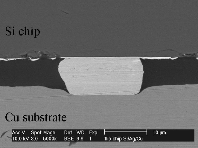
18 Si bonded to Cu: cross section SEM Si (Ag)+Ag Si Ag-In Ag 2 In (Ag) +Ag 46um Cu Cu
 8μm")
+ Ag Cu")
19 Si bonded to Cu: EDX analysis of the joint Si +15 Ag+(Ag) 8μm Ag 2 In (Ag) +Ag (Ag)+ Ag 8μm Ag 2 In interface (Ag)+ Ag Cu -20
20 Outline Solders and Soldering Fluxless Soldering: 3 methods An example: Fluxless Ag-In Bonding Solid State Atomic Bonding Solder Flip-Chip Technology Silver Flip-Chip Technology Summary
21 Solid-state Silver Bonding The fundamental belief: - When A atoms and B atoms are brought within atomic distance so that they see each other, bonding will occur provided that they agree to share electrons. The challenge: - How to bring A atoms and B atoms within atomic range on the bonding interface? Approach: - Deformation of material A so that it conforms to and follow the surface of material B - What needed: pressure, temperature & clean surfaces
22 Conventional compression bonding methods Laminated metal Procedure Note [1] Ti to Al Cold roll at R.T. 50% reduction in thickness [2] Ni to Pd-25wt.% Ag Cold roll at R.T. [3] Cu to LCP Surface activation Cold roll at R.T. 75% reduction in thickness Cold roll under pressure of 46,400 psi In our process: 260 o C at 1,000psi (6.9 MPa) for 4 minutes We believe: they bond in seconds or less [1] J. G. Luo and Viola L. Acoff, Using cold roll bonding and annealing to process Ti/Al multi-layered composites from elemental foils, Materials Science and Engineering A, 379, pp , 2004 [2] S. Tosti, Supported and laminated Pd-based metallic membranes, International Journal of Hydrogen Energy, 28, pp , 2003 [3] Kouji Nanbu, Shinji Ozawa, Kazuo Yoshida et al., Low temperature bonded Cu/LCP materials for FPCs and their characteristics, IEEE Transactions on Components and Packaging Technologies, 28, pp.760, 2005

23 Bonding design I: Si-Ag foil-cu One step Bonding Si chip + Ag foil + Cu substrate Cr/Au Ag foil Si chip Cu substrate Si chip Ag foil Ag foil Cu substrate


24 Bonding design II: Si Ag(plated) on Cu Bonding structure Si chip + Post-annealed plated Ag Cu substrate Cr/Au Si chip plated Ag Cu substrate Si chip plated Ag plated Ag Cu substrate


25 Microstructure of plated Ag Hall-Petch Eq: σ y =σ o + k y *d -1/2 d: average grain diameter σ y : yield strength σ o and k: material parameters as-plated after o C for 3hrs

26 Shear strength: Si-Ag interface Shear test Sample E Si chip Ag foil Copper Test speed: 300µm/sec Ag foil Copper - All Si chips broke except Sample D - Fracture interface is inside Si 5mm Failure force Sample Fracture force A 51.5 Kg B 29.3 Kg C 32.4 Kg D 10.8 Kg E 22.4 Kg MIL-STD-883G: 5 Kg

27 Force (Kg) Shear strength: Ag-Cu interface Shear test Sample A Ag foil Copper Ag foil Copper Test speed:300µm/sec - Ag foil yields - Fracture interface is inside bulk Ag 5mm Force vs. Distance Failure force Sample Failure force A 59.8 Kg B 57.5 Kg 60 Ag(A) Ag(B) Distance (um)
28 Outline Solders and Soldering Fluxless Soldering: 3 methods An example: Fluxless Ag-In Bonding Solid State Atomic Bonding Solder Flip-Chip Technology Silver Flip-Chip Technology Summary
29 Solder flip chip interconnect Thermal interface material Heat spreader Silicon chip Underfill Lid sealant Package substrate PCB Solder Silicon chip Solder UBM 1 IMC 1 Solder UBM1 Materials Sn-Ag-Cu Ni/Au or Ni/Cu Package substrate IMC 2 UBM 2 IMC1 UBM2 Ni 3 Sn 4 or Cu 6 Sn 5 Ni/Au Solder Solder IMC 2 IMC2 Cu 6 Sn 5 or Ni 3 Sn 4 PCB IMC 3 UBM 3 UBM3 IMC3 Cu Cu 6 Sn 5 29

 solder reaction in flip chip technology, Mater. Sci. Eng. R., Vol. 34, pp. 1-58, 2001.")

30 Flip chip solder joints Ref: C. Chen, H. M. Tong, and K. N. Tu, Electromigration and Thermomigration in Pb-free Flip Chip Solder Joints, Annu. Rev. Mater. Res., vol. 40, pp , Ref: K. N. Tu and K. Zheng, Tin-lead (SnPb) solder reaction in flip chip technology, Mater. Sci. Eng. R., Vol. 34, pp. 1-58, μm pad 40μm pad 20μm pad 10μm pad μm pitch 60μm pitch 40μm pitch 20μm pitch Ref: K. O donnell, UBM: Creating the Critical Interface, Available Online,


31 Ref: J. W. Nah and K. N. Tu, Electromigration in flip chip solder joint, Lead-free technology workshop, TMS Annual Meeting, San Francisco, CA, 2005.


32 Ref: H. Ye, C. Basaran, and D. C. Hopkins, Mechanical Implications of High Current Densities in Flip Chip Solder Joints, IMECE, pp , ASME, Ref: C. Basaran, H. Ye, D. C. Hopkins, D. Frear, and J.K. Lin, Flip Chip Solder Joint Failure Modes, Available Online, display/238913/articles/advanced-packaging/volume-14/issue- 10/features/flip-chip-solder-joint-failure-modes.html Ref: D. R. Frear, Materials Issues in Area-Array Microelectronic Packaging, JOM, vol. 51, no. 3, pp , 1999.


33 Optical Image: solder balls Sn-37Pb Sn-0.7Cu Sn-3.5Ag Sn-3.8Ag-0.3Cu Ref: D. R. Frear, J. W. Jang, J. K. Lin, and C. Zhang, Pb-Free Solders for Flip-Chip Interconnects, JOM, vol. 51, no. 6, pp , 2001.
34 Solder flip chip joints: Analysis ϕ UBM h Cu Si Package UBM: under bump metallurgy IMC: intermetalic compound layer IMC 1 h s IMC 2 h = joint height, h s = solder height Δs Shear strain: ε sh = Δs/h s Solder aspect ratio: γ s = h s /ϕ < 0.7 As ϕ -> h s & ε sh As time -> h s & ε sh As ϕ -> R solder = (ρ)(4h/πϕ 2 ) = (ρ)(4/π)(h/ϕ)(1/ϕ)
35 Outline Solders and Soldering Fluxless Soldering: 3 methods A UCI example: Fluxless Ag-In Bonding Solid State Atomic Bonding Solder Flip-Chip Technology Silver Flip-Chip Technology Summary
36 Silver flip-chip interconnect Why silver? It is simply the best choice. Challenge: How to bond silver without it melting? Answer: Solid state atomic bonding.
37 Properties of relevant materials Properties Copper Silver Gold Tin 96.5Sn3.5Ag Melting Point ( o C) 1, , Density (g/cc) Thermal conductivity (watt/cm-k) Electrical Conductivity (/Ωcm) Thermal Expansion Coeff. (/k) x x x x x x x x x x10-6 Yield Strength (psi) 10,000 1, ,300 3,600 Ultimate Tensile Strength (psi) 32,000 21,000 17,000 2,000 5,000~7,000 Young s modulus (psi) 1.92x x x x x10 6 Elongation at break (%) ~80 37 Hardness (Brinell)


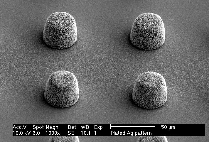
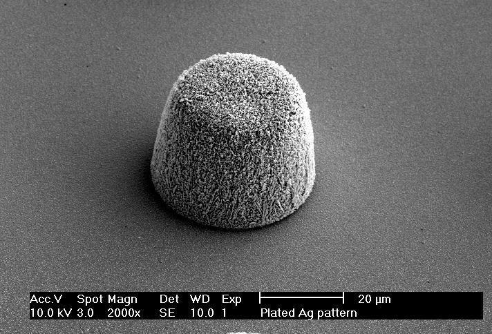
38 40µm Ag columns on Si/Cr/Au


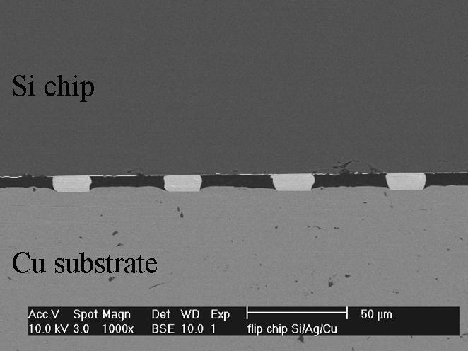
39 Si with Ag columns bonded to Cu: I Peak temperature: 270 o C, Pressure applied: 960psi Si chip Si chip Ag Cu substrate Cu Cu substrate Si chip Ag Si chip Cu substrate Cu Cu substrate


40 Si with Ag columns bonded to Cu: II Peak temperature: 270 o C, Pressure applied: 760psi Si chip Si chip Cu substrate Cu substrate Si chip Si chip Cu substrate Cu substrate


41 Si with Ag columns bonded to Cu: III Peak temperature: 260 o C, Pressure applied: 680psi Si chip Si chip Cu substrate Cu substrate Si Si chip Si chip Ag Cu Cu substrate Cu substrate
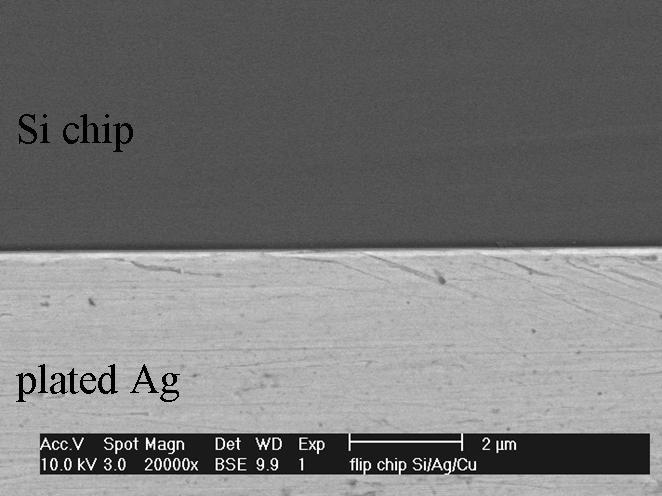
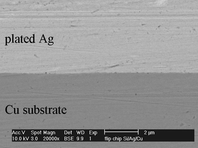
42 Bonding interfaces High magnification SEM images on interfaces Si/Cr/Au/Ag Ag/Cu Si chip Ag Ag Cu substrate

43 Bonding interfaces Are they really bonded or just mechanical interlocking? Si/Cr/Au/Ag Ag/Cu Si chip Ag Ag Cu substrate


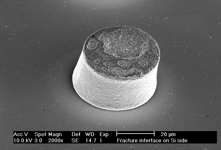
44 Fracture of 40µm Ag flip chip joints Sample with 50x50 array withstands at least 6.3kg pull force (MIL-STD-883E failure force:1.93kg). Broke by shear&pull Fracture surface on Cu side 44


45 Fracture modes: Cu side I II b II a III Si Fracture modes I. Ag-Cu interface: No Ag stays on Cu II. Within Ag column: a. Most Ag column stays on Cu b. Small portion of Ag stays on Cu III. Within Si chip: Nearly all Ag column with Si piece stays on Cu 45


46 Fracture modes: Si side III II a II a II b II b III 46

47 15µm Ag flip chip interconnect Total pressure = 800psi, 0.1gm per column, 125x125 array 47
48 Outline Solders and Soldering Fluxless Soldering: 3 methods A example: Fluxless Ag-In Bonding Solid State Atomic Bonding Solder Flip-Chip Technology Silver Flip-Chip Technology Summary
49 Potential Advantages of Ag flip-chip: In random order High electrical conductivity, 7.7 times of that of Pb-free solders. High thermal conductivity, 5.2 times of that of Pb-free solders. No flux; completely fluxless. No IMCs; issues associated with IMC & IMC growth do not exist. No solder mask needed. No molten phase involved; the bump can better keep its shape and geometry. No molten phase involved; bridging of adjacent bumps does not occur. Ductile Ag manages CTE mismatch between chips & packages. Ag joints have high melting temperature, 961ºC. Aspect ratio of bumps can be greater than 1. Alignment tolerance: up to ¼ pitch The size of columns is only limited by the lithographic process. Yet to be identified.
50 Thank you. Questions?
An Innovative High Throughput Thermal Compression Bonding Process
 An Innovative High Throughput Thermal Compression Bonding Process Li Ming 2 September 2015 Outline Introduction Throughput improved TCB Process Liquid Phase Contact (LPC) bonding Flux-LPC-TCB under inert
Lead-Free Solder Bump Technologies for Flip-Chip Packaging Applications
 Lead-Free Solder Bump Technologies for Flip-Chip Packaging Applications Zaheed S. Karim 1 and Jim Martin 2 1 Advanced Interconnect Technology Ltd. 1901 Sunley Centre, 9 Wing Yin Street, Tsuen Wan, Hong
Electromigration failure mechanisms for SnAg3.5 solder bumps on Ti/Cr-Cu/Cu and Ni P /Au metallization pads
 JOURNAL OF APPLIED PHYSICS VOLUME 96, NUMBER 8 15 OCTOBER 2004 Electromigration failure mechanisms for SnAg3.5 solder bumps on Ti/Cr-Cu/Cu and Ni P /Au metallization pads T. L. Shao, Y. H. Chen, S. H.
Thermo-Mechanical FEM Analysis of Lead Free and Lead Containing Solder for Flip Chip Applications
 Thermo-Mechanical FEM Analysis of Lead Free and Lead Containing Solder for Flip Chip Applications M. Gonzalez 1, B. Vandevelde 1, Jan Vanfleteren 2 and D. Manessis 3 1 IMEC, Kapeldreef 75, 3001, Leuven,
Micro-Impact Test on Lead-Free BGA Balls on Au/Electrolytic Ni/Cu Bond Pad
 Micro- Test on Lead-Free BGA Balls on Au/Electrolytic Ni/Cu Bond Pad Shengquan Ou*, Yuhuan Xu and K. N. Tu Department of Materials Science and Engineering, UCLA, Los Angeles, CA, 90095-1595 M. O. Alam,
Interfacial reactions of BGA Sn 3.5%Ag 0.5%Cu and Sn 3.5%Ag solders during high-temperature aging with Ni/Au metallization
 Materials Science and Engineering B 113 (2004) 184 189 Interfacial reactions of BGA Sn 3.5%Ag 0.5%Cu and Sn 3.5%Ag solders during high-temperature aging with Ni/Au metallization Ahmed Sharif, M.N. Islam,
Electromigration in Flip Chip Solder Joints
 Electromigration in Flip Chip Solder Joints K.N. Tu Dept. of Materials Science & Engineering, UCLA 1. Introduction 2. Why does electromigration in solder joint become a reliability problem? 3. Electromigration
1 Thin-film applications to microelectronic technology
 1 Thin-film applications to microelectronic technology 1.1 Introduction Layered thin-film structures are used in microelectronic, opto-electronic, flat panel display, and electronic packaging technologies.
Interfacial reactions of Sn Cu solder with Ni/Au surface finish on Cu pad during reflow and aging in ball grid array packages
 Materials Science and Engineering B 117 (2005) 246 253 Interfacial reactions of Sn Cu solder with Ni/Au surface finish on Cu pad during reflow and aging in ball grid array packages M.N. Islam, Y.C. Chan
Study of the Interface Microstructure of Sn-Ag-Cu Lead-Free Solders and the Effect of Solder Volume on Intermetallic Layer Formation.
 Study of the Interface Microstructure of Sn-Ag-Cu Lead-Free Solders and the Effect of Solder Volume on Intermetallic Layer Formation. B. Salam +, N. N. Ekere, D. Rajkumar Electronics Manufacturing Engineering
WF6317. A superactive low-volatile/high heat-resistant water-soluble flux for ball soldering
 WF637 A superactive low-volatile/high heat-resistant water-soluble flux for ball soldering Low viscosity and high tacking power stabilize ball holding force and ensures excellent solder wettability Easy
Manufacturing and Reliability Modelling
 Manufacturing and Reliability Modelling Silicon Chip C Bailey University of Greenwich London, England Printed Circuit Board Airflow Temperature Stress at end of Reflow Stress Product Performance in-service
Thermomigration and electromigration in Sn58Bi ball grid array solder joints
 J Mater Sci: Mater Electron (2010) 21:1090 1098 DOI 10.1007/s10854-009-9992-2 Thermomigration and electromigration in Sn58Bi ball grid array solder joints X. Gu K. C. Yung Y. C. Chan Received: 18 August
Copyright 2008 Year IEEE. Reprinted from IEEE ECTC May 2008, Florida USA.. This material is posted here with permission of the IEEE.
 Copyright 2008 Year IEEE. Reprinted from IEEE ECTC 2008. 27-30 May 2008, Florida USA.. This material is posted here with permission of the IEEE. Such permission of the IEEE does not in any way imply IEEE
Interfacial Reactions between the Sn-9Zn Solder and Au/Ni/SUS304 Multi-layer Substrate
 , July 6-8, 2011, London, U.K. Interfacial Reactions between the Sn-9Zn Solder and Au/Ni/SUS304 Multi-layer Substrate *Yee-Wen Yen 1, Chien-Chung Jao 2, Kuo-Sing Chao 1, Shu-Mei Fu Abstract Sn-9Zn lead-free
SCV Chapter, CPMT Society, IEEE September 14, Voids at Cu / Solder Interface and Their Effects on Solder Joint Reliability
 Voids at / Solder Interface and Their Effects on Solder Joint Reliability Zequn Mei, Mudasir Ahmad, Mason Hu, Gnyaneshwar Ramakrishna Manufacturing Technology Group Cisco Systems, Inc. Acknowledgement:
Jeong et al.: Effect of the Formation of the Intermetallic Compounds (1/7)
") Jeong et al.: Effect of the Formation of the Intermetallic Compounds (1/7) Effect of the Formation of the Intermetallic Compounds between a Tin Bump and an Electroplated Copper Thin Film on both the Mechanical
Jeong et al.: Effect of the Formation of the Intermetallic Compounds (1/7) Effect of the Formation of the Intermetallic Compounds between a Tin Bump and an Electroplated Copper Thin Film on both the Mechanical
Recrystallization Effect and Electric Flame-Off Characteristic of Thin Copper Wire
 Materials Transactions, Vol. 47, No. 7 (2006) pp. 1776 to 1781 #2006 The Japan Institute of Metals Recrystallization Effect and Electric Flame-Off Characteristic of Thin Copper Wire Fei-Yi Hung*, Yuan-Tin
Composition/wt% Bal SA2 (SABI) Bal SA3 (SABI + Cu) Bal
 Bal SA3 (SABI + Cu) Bal") Improving Thermal Cycle and Mechanical Drop Impact Resistance of a Lead-free Tin-Silver-Bismuth-Indium Solder Alloy with Minor Doping of Copper Additive Takehiro Wada 1, Seiji Tsuchiya 1, Shantanu Joshi
Improving Thermal Cycle and Mechanical Drop Impact Resistance of a Lead-free Tin-Silver-Bismuth-Indium Solder Alloy with Minor Doping of Copper Additive Takehiro Wada 1, Seiji Tsuchiya 1, Shantanu Joshi
Dissolution of electroless Ni metallization by lead-free solder alloys
 Journal of Alloys and Compounds 388 (2005) 75 82 Dissolution of electroless Ni metallization by lead-free solder alloys Ahmed Sharif, Y.C. Chan, M.N. Islam, M.J. Rizvi Department of Electronic Engineering,
Fluxless Process of Fabricating In Au Joints on Copper Substrates
 IEEE TRANSACTIONS ON COMPONENTS AND PACKAGING TECHNOLOGIES, VOL. 23, NO. 2, JUNE 2000 377 Fluxless Process of Fabricating In Au Joints on Copper Substrates William W. So and Chin C. Lee, Senior Member,
Failure Modes of Flip Chip Solder Joints Under High Electric Current Density
 C. Basaran e-mail: cjb@buffalo.edu H. Ye D. C. Hopkins Electronic Packaging Laboratory, University at Buffalo, SUNY, Buffalo, New York D. Frear J. K. Lin Freescale semiconductor Inc., Tempe, Arizona Failure
Electric Flame-Off Characteristics and Fracture Properties of 20 m Thin Copper Bonding Wire
 Materials Transactions, Vol. 5, No. 2 (29) pp. 293 to 298 #29 The Japan Institute of Metals Electric Flame-Off Characteristics and Fracture Properties of 2 m Thin Copper Bonding Wire Fei-Yi Hung 1; *,
LS720V Series. Comparison of crack progression between Sn-Cu-Ni-Ge and M773. Development of Ag-free/M773 alloy
 LS72V Series Low-Ag/Ag-free solder pastes with lower void Reduces voids by improving fluidity of flux during solder melting Reduces voids even in bottom surface electrode type components by improving solder
Effect of Magnesium Addition on Microstructure and Mechanical Properties of Lead-Free Zinc-Silver Solder Alloys
 Effect of Magnesium Addition on Microstructure and Mechanical Properties of Lead-Free Zinc-Silver Solder Alloys Md. Anisul Islam * and Ahmed Sharif Department of Materials and Metallurgical Engineering,
Influence of Thermomigration on Lead-Free Solder Joint Mechanical Properties
 Mohd F. Abdulhamid Cemal Basaran 1 e-mail: cjb@buffalo.edu Electronic Packaging Laboratory, University at Buffalo, SUNY, Buffalo, NY 14260 Influence of Thermomigration on Lead-Free Solder Joint Mechanical
Jacques Matteau. NanoBond Assembly: A Rapid, Room Temperature Soldering Process. Global Sales Manager. indium.us/f018
 Jacques Matteau Global Sales Manager NanoBond Assembly: A Rapid, Room Temperature Soldering Process jmatteau@indium.com indium.us/f014 indium.us/f018 Terminology A few key terms NanoFoil is the heat source
Advanced Analytical Techniques for Semiconductor Assembly Materials and Processes. Jason Chou and Sze Pei Lim Indium Corporation
 Advanced Analytical Techniques for Semiconductor Assembly Materials and Processes Jason Chou and Sze Pei Lim Indium Corporation Agenda Company introduction Semiconductor assembly roadmap challenges Fine
Low Cycle Fatigue Testing of Ball Grid Array Solder Joints under Mixed-Mode Loading Conditions
 Tae-Sang Park Mechatronics & Manufacturing Technology Center, Corporate Technology Operations, Samsung Electronics Co., LTD, 416, Maetan-3Dong, Yeongtong-Gu, Suwon-City, Gyeonggi-Do, 443-742, Korea e-mail:
Packaging Effect on Reliability for Cu/Low k Damascene Structures*
 Packaging Effect on Reliability for Cu/Low k Damascene Structures* Guotao Wang and Paul S. Ho Laboratory of Interconnect & Packaging, TX 78712 * Work supported by SRC through the CAIST Program TRC 2003
Effects of Lead on Tin Whisker Elimination
 Effects of Lead on Tin Whisker Elimination Wan Zhang and Felix Schwager Rohm and Haas Electronic Materials Lucerne, Switzerland inemi Tin Whisker Workshop at ECTC 0 May 30, 2006, in San Diego, CA Efforts
A Roadmap to Low Cost Flip Chip Technology and Chip Size Packaging using Electroless Nickel Gold Bumping
 A Roadmap to Low Cost Flip Chip Technology and Chip Size Packaging using Electroless Nickel Gold Bumping T. Oppert, T. Teutsch, E. Zakel Pac Tech Packaging Technologies GmbH Am Schlangenhorst 15-17, Germany
System Level Effects on Solder Joint Reliability
 System Level Effects on Solder Joint Reliability Maxim Serebreni 2004 2010 Outline Thermo-mechanical Fatigue of solder interconnects Shear and tensile effects on Solder Fatigue Effect of Glass Style on
Microelectronics Reliability
 Microelectronics Reliability 49 (2009) 269 287 Contents lists available at ScienceDirect Microelectronics Reliability journal homepage: www.elsevier.com/locate/microrel Interfacial fracture toughness of
3D-WLCSP Package Technology: Processing and Reliability Characterization
 3D-WLCSP Package Technology: Processing and Reliability Characterization, Paul N. Houston, Brian Lewis, Fei Xie, Ph.D., Zhaozhi Li, Ph.D.* ENGENT Inc. * Auburn University ENGENT, Inc. 2012 1 Outline Packaging
Controlling the Microstructures from the Gold-Tin Reaction
 Controlling the Microstructures from the Gold-Tin Reaction J. Y. Tsai, C. W. Chang, Y. C. Shieh, Y. C. Hu, and C. R. Kao* Department of Chemical & Materials Engineering National Central University Chungli
Metals I. Anne Mertens
 "MECA0139-1: Techniques "MECA0462-2 additives : et Materials 3D printing", Selection", ULg, 19/09/2017 25/10/2016 Metals I Anne Mertens Introduction Outline Metallic materials Materials Selection: case
The Morphology Evolution and Voiding of Solder Joints on QFN Central Pads with a Ni/Au Finish
 The Morphology Evolution and Voiding of Solder Joints on QFN Central Pads with a Ni/Au Finish Julie Silk 1, Jianbiao Pan 2, Mike Powers 1 1 Agilent Technologies, 1400 Fountaingrove Parkway, Santa Rosa,
SLID bonding for thermal interfaces. Thermal performance. Technology for a better society
 SLID bonding for thermal interfaces Thermal performance Outline Background and motivation The HTPEP project Solid-Liquid Inter-Diffusion (SLID) Au-Sn SLID Cu-Sn SLID Reliability and bond integrity Alternative
Analysis of plating grain size effect on whisker
 Journal of Mechanical Science and Technology 23 (2009) 2885~2890 Journal of Mechanical Science and Technology www.springerlink.com/content/1738-494x DOI 10.1007/s12206-009-0720-x Analysis of plating grain
Electromigration Behavior of through-si-via (TSV) Interconnect for 3-D Flip Chip Packaging
 Interconnect for 3-D Flip Chip Packaging") Materials Transactions, Vol. 51, No. 5 (2010) pp. 1020 to 1027 #2010 The Japan Institute of Metals EXPRESS REGULAR ARTICLE Electromigration Behavior of through-si-via (TSV) Interconnect for 3-D Flip Chip
Materials Transactions, Vol. 51, No. 5 (2010) pp. 1020 to 1027 #2010 The Japan Institute of Metals EXPRESS REGULAR ARTICLE Electromigration Behavior of through-si-via (TSV) Interconnect for 3-D Flip Chip
Atmosphere Effect on Soldering of Flip Chip Assemblies. C. C. Dong Air Products and Chemicals, Inc. U.S.A.
 Atmosphere Effect on Soldering of Flip Chip Assemblies C. C. Dong Air Products and Chemicals, Inc. U.S.A. Atmosphere Effect on Soldering of Flip Chip Assemblies Abstract An experimental study was conducted
curamik CERAMIC SUBSTRATES AMB technology Design Rules Version #04 (09/2015)
") curamik CERAMIC SUBSTRATES AMB technology Design Rules Version #04 (09/2015) Content 1. Geometric properties 1.01. Available ceramic types / thicknesses... 03 1.02. thicknesses (standard)... 03 3. Quality
curamik CERAMIC SUBSTRATES AMB technology Design Rules Version #04 (09/2015) Content 1. Geometric properties 1.01. Available ceramic types / thicknesses... 03 1.02. thicknesses (standard)... 03 3. Quality
Reflow Profiling: Time a bove Liquidus
 Reflow Profiling: Time a bove Liquidus AIM/David Suraski Despite much research and discussion on the subject of reflow profiling, many questions and a good deal of confusion still exist. What is clear
Evaluation of Cu Pillar Chemistries
 Presented at 2016 IMAPS Device Packaging Evaluation of Cu Pillar Chemistries imaps Device Packaging Conference Spring 2016 Matthew Thorseth, Mark Scalisi, Inho Lee, Sang-Min Park, Yil-Hak Lee, Jonathan
Non-Conductive Adhesive (NCA) Trapping Study in Chip on Glass Joints Fabricated Using Sn Bumps and NCA
 Trapping Study in Chip on Glass Joints Fabricated Using Sn Bumps and NCA") Materials Transactions, Vol. 49, No. 9 (2008) pp. 2100 to 2106 #2008 The Japan Institute of Metals Non-Conductive Adhesive (NCA) Trapping Study in Chip on Glass Joints Fabricated Using Sn Bumps and NCA
Materials Transactions, Vol. 49, No. 9 (2008) pp. 2100 to 2106 #2008 The Japan Institute of Metals Non-Conductive Adhesive (NCA) Trapping Study in Chip on Glass Joints Fabricated Using Sn Bumps and NCA
EFFECT OF Ag COMPOSITION, DWELL TIME AND COOLING RATE ON THE RELIABILITY OF Sn-Ag-Cu SOLDER JOINTS. Mulugeta Abtew
 EFFECT OF Ag COMPOSITION, DWELL TIME AND COOLING RATE ON THE RELIABILITY OF Sn-Ag-Cu SOLDER JOINTS Mulugeta Abtew Typical PCB Assembly Process PCB Loading Solder Paste Application Solder Paste Inspection
DEVELOPMENT OF LEAD-FREE ALLOYS WITH ULTRA-HIGH THERMO- MECHANICAL RELIABILITY
 As originally published in the SMTA Proceedings. DEVELOPMENT OF LEAD-FREE ALLOYS WITH ULTRA-HIGH THERMO- MECHANICAL RELIABILITY Pritha Choudhury, Ph.D., Morgana Ribas, Ph.D., Ranjit Pandher, Ph.D., Anil
Effect of Surface Finishes on Ball Shear Strength in BGA Joints with Sn 3.5 mass%ag Solder
 Materials Transactions, Vol. 43, No. 4 (2002) pp. 751 to 756 c 2002 The Japan Institute of Metals EXPRESS REGULR RTICLE Effect of Surface Finishes on all Shear Strength in G Joints with Sn 3.5 mass%g Solder
Self-Organized Interconnection Process Using Solderable ACA (Anisotropic Conductive Adhesive)
") Materials Transactions, Vol. 50, No. 7 (2009) pp. 1684 to 1689 Special Issue on New Functions and Properties of Engineering Materials Created by Designing and Processing #2009 The Japan Institute of Metals
Materials Transactions, Vol. 50, No. 7 (2009) pp. 1684 to 1689 Special Issue on New Functions and Properties of Engineering Materials Created by Designing and Processing #2009 The Japan Institute of Metals
Flip Chip - Integrated In A Standard SMT Process
 Flip Chip - Integrated In A Standard SMT Process By Wilhelm Prinz von Hessen, Universal Instruments Corporation, Binghamton, NY This paper reviews the implementation of a flip chip product in a typical
Plasma for Underfill Process in Flip Chip Packaging
 Plasma for Underfill Process in Flip Chip Packaging Jack Zhao and James D. Getty Nordson MARCH 2470-A Bates Avenue Concord, California 94520-1294 USA Published by Nordson MARCH www.nordsonmarch.com 2015
A Study of the Effect of Indium Filler Metal on the Bonding Strength of Copper and Tin
 Koyama et al.: A Study of the Effect of Indium Filler Metal (1/6) [Technical Paper] A Study of the Effect of Indium Filler Metal on the Bonding Strength of Copper and Tin Shinji Koyama, Seng Keat Ting,
High-Temperature-Resistant Interconnections Formed by Using Nickel Micro-plating and Ni Nano-particles for Power Devices
 Kato et al.: High-Temperature-Resistant Interconnections (1/6) [Technical Paper] High-Temperature-Resistant Interconnections Formed by Using Nickel Micro-plating and Ni Nano-particles for Power Devices
Fluxless soldering using Electron Attachment (EA) Technology
 Technology") Fluxless soldering using Electron Attachment (EA) Technology Proprietary, patented innovation for wafer level packaging applications including wafer bump and copper pillar reflow. Air Products has partnered
Fluxless soldering using Electron Attachment (EA) Technology Proprietary, patented innovation for wafer level packaging applications including wafer bump and copper pillar reflow. Air Products has partnered
Unique Failure Modes from use of Sn-Pb and Lead-Free (mixed metallurgies) in PCB Assembly: CASE STUDY
 in PCB Assembly: CASE STUDY") Unique Failure Modes from use of Sn-Pb and Lead-Free (mixed metallurgies) in PCB Assembly: CASE STUDY Frank Toth, and Gary F. Shade; Intel Corporation, Hillsboro, OR, USA {francis.toth.jr@intel.com, (503)-696-1546}
Unique Failure Modes from use of Sn-Pb and Lead-Free (mixed metallurgies) in PCB Assembly: CASE STUDY Frank Toth, and Gary F. Shade; Intel Corporation, Hillsboro, OR, USA {francis.toth.jr@intel.com, (503)-696-1546}
Ultra Fine Pitch Bumping Using e-ni/au and Sn Lift-Off Processes
 Ultra Fine Pitch Bumping Using e-ni/au and Sn Lift-Off Processes Andrew Strandjord, Thorsten Teutsch, and Jing Li Pac Tech USA Packaging Technologies, Inc. Santa Clara, CA USA 95050 Thomas Oppert, and
IBM Research Report. Yoon-Chul Sohn, Jin Yu KAIST 373-1, Guseong-Dong, Yuseong-Gu Daejeon Korea
 RC23513 (W0502-039) February 4, 2005 Materials Science IBM Research Report Effect of Intermetallics Spalling on the Mechanical Behavior of Electroless Ni(P)/Pb-free Solder Interconnection Yoon-Chul Sohn,
Cu Pillar Interconnect and Chip-Package-Interaction (CPI) for Advanced Cu Low K chip
 for Advanced Cu Low K chip") EPRC 12 Project Proposal Cu Pillar Interconnect and Chip-Package-Interaction (CPI) for Advanced Cu Low K chip 15 th Aug 2012 Page 1 Introduction: Motivation / Challenge Silicon device with ultra low k
EPRC 12 Project Proposal Cu Pillar Interconnect and Chip-Package-Interaction (CPI) for Advanced Cu Low K chip 15 th Aug 2012 Page 1 Introduction: Motivation / Challenge Silicon device with ultra low k
Lead Free No Clean Solder Paste 4900P Technical Data Sheet 4900P
 Description MG Chemicals has developed a unique flux system designed specifically for high temperature lead free alloys. It provides the fluxing activity levels that promote thermal stability and prevents
Advances in Printing nano Cu and Using Existing Cu Based Manufacturing Processes. Michael J. Carmody Chief Scientist, Intrinsiq Materials
 Advances in Printing nano Cu and Using Existing Cu Based Manufacturing Processes Michael J. Carmody Chief Scientist, Intrinsiq Materials Why Use Copper? Lower Cost than Silver. Print on Numerous Substrates.
Introduction to the phase diagram Uses and limitations of phase diagrams Classification of phase diagrams Construction of phase diagrams
 Prof. A.K.M.B. Rashid Department of MME BUET, Dhaka Concept of alloying Classification of alloys Introduction to the phase diagram Uses and limitations of phase diagrams Classification of phase diagrams
A STUDY OF THE ENEPIG IMC FOR EUTECTIC AND LF SOLDERS
 A STUDY OF THE ENEPIG IMC FOR EUTECTIC AND LF SOLDERS G.Milad, D.Gudeczauskas, G.Obrien, A.Gruenwald Uyemura International Corporation Southington, CT ABSTRACT: The solder joint formed on an ENEPIG surface
TSV Processing and Wafer Stacking. Kathy Cook and Maggie Zoberbier, 3D Business Development
 TSV Processing and Wafer Stacking Kathy Cook and Maggie Zoberbier, 3D Business Development Outline Why 3D Integration? TSV Process Variations Lithography Process Results Stacking Technology Wafer Bonding
Ultralow Residue Semiconductor Grade Fluxes for Copper Pillar Flip-Chip
 Ultralow Residue Semiconductor Grade Fluxes for Copper Pillar Flip-Chip SzePei Lim (Presenter), Jason Chou, Maria Durham, and Dr. Andy Mackie Indium Corporation 1 Outline of Presentation Roadmaps and challenges
Effects of Design, Structure and Material on Thermal-Mechanical Reliability of Large Array Wafer Level Packages
 Effects of Design, Structure and Material on Thermal-Mechanical Reliability of Large Array Wafer Level Packages Bhavesh Varia 1, Xuejun Fan 1, 2, Qiang Han 2 1 Department of Mechanical Engineering Lamar
Synchrotron Radiation X-Ray Microdiffraction of Pb-free solders
 Synchrotron Radiation X-Ray Microdiffraction of Pb-free solders Advanced Light Source, Lawrence Berkeley National Laboratory Collaborators: W.J. Choi, T.Y. Lee, A. Wu, K.-N. Tu, UCLA W.A. Caldwell, R.
DSP 615D (Sn63/Pb37) NO CLEAN DISPENSING SOLDER PASTE
 NO CLEAN DISPENSING SOLDER PASTE") SN/AG/CU. 862 Rev.A TECHNICAL DATA SHEET TECHNICAL SPECIFICATIONS SN/AG/CU. 862 Rev DSP 615D (Sn63/Pb37) NO CLEAN DISPENSING SOLDER PASTE CORPORATE HEADQUARTERS USA: 315 Fairbank St. Addison, IL 60101!
SN/AG/CU. 862 Rev.A TECHNICAL DATA SHEET TECHNICAL SPECIFICATIONS SN/AG/CU. 862 Rev DSP 615D (Sn63/Pb37) NO CLEAN DISPENSING SOLDER PASTE CORPORATE HEADQUARTERS USA: 315 Fairbank St. Addison, IL 60101!
Solder joint reliability of cavity-down plastic ball grid array assemblies
 cavity-down plastic ball grid array S.-W. Ricky Lee Department of Mechanical Engineering, The Hong Kong University of Science and, Kowloon, Hong Kong John H. Lau Express Packaging Systems, Inc., Palo Alto,
IEEE TRANSACTIONS ON COMPONENTS, PACKAGING, AND MANUFACTURING TECHNOLOGY PART B, VOL. 20, NO. 1, FEBRUARY
 IEEE TRANSACTIONS ON COMPONENTS, PACKAGING, AND MANUFACTURING TECHNOLOGY PART B, VOL. 20, NO. 1, FEBRUARY 1997 87 Effect of Intermetallic Compounds on the Thermal Fatigue of Surface Mount Solder Joints
Aging Treatment Characteristics of Shear Strength in Micro Solder Bump
 Materials Transactions, Vol. 43, No. 2 (22) pp. 3234 to 3238 c 22 The Japan Institute of Metals Aging Treatment Characteristics of Shear Strength in Micro Solder Bump Chong-Hee Yu, Kyung-Seob Kim 2, Yong-Bin
UTILIZATION OF ATMOSPHERIC PLASMA SURFACE PREPARATION TO IMPROVE COPPER PLATING PROCESSES.
 SESSION 14 MATERIALS AND PROCESSES FOR ADVANCED PACKAGING UTILIZATION OF ATMOSPHERIC PLASMA SURFACE PREPARATION TO IMPROVE COPPER PLATING PROCESSES. Eric Schulte 1, Gilbert Lecarpentier 2 SETNA Corporation
Failure Modes in Wire bonded and Flip Chip Packages
 Failure Modes in Wire bonded and Flip Chip Packages Mumtaz Y. Bora Peregrine Semiconductor San Diego, Ca. 92121 mbora@psemi.com Abstract The growth of portable and wireless products is driving the miniaturization
The Effect of Cu and Ni on the Structure and Properties of the IMC Formed by the Reaction of Liquid Sn-Cu Based Solders with Cu Substrate
 WDS'08 Proceedings of Contributed Papers, Part III, 220 224, 2008. ISBN 978-80-7378-067-8 MATFYZPRESS The Effect of Cu and Ni on the Structure and Properties of the IMC Formed by the Reaction of Liquid
Field Condition Reliability Assessment for SnPb and SnAgCu Solder Joints in Power Cycling Including Mini Cycles
 Field Condition Reliability Assessment for SnPb and SnAgCu Solder Joints in Power Cycling Including Mini Cycles Min Pei 1, Xuejun Fan 2 and Pardeep K. Bhatti 2 1 Georgia Tech, 801 Ferst Dr. NW, Atlanta,
Kyoung-Soon Bok, Woo-Suk Choi, and Chul-Lae Cho Samsung Techwin co., LTD. 14 Nongseo-Ri, Kiheung-Eub, Youngin-Si, Kyoungki-Do, , Korea
 Studies on Ni-Sn Intermetallic Compound and P-rich Ni Layer at the ckel UBM - Solder Interface and Their Effects on Flip Chip Solder Joint Reliability Young-Doo Jeon and Kyung-Wook Paik Micro-Electronic
Arch. Metall. Mater. 62 (2017), 2B,
, 2B,") Arch. Metall. Mater. 62 (2017), 2B, 1027-1031 DOI: 10.1515/amm-2017-0147 D. KONCZ-HORVÁTH*#, G. GERGELY*, Z. GÁCSI* WHISKER-LIKE FORMATIONS IN Sn-3.0Ag-Pb ALLOYS In this study, different types of whisker-like
Arch. Metall. Mater. 62 (2017), 2B, 1027-1031 DOI: 10.1515/amm-2017-0147 D. KONCZ-HORVÁTH*#, G. GERGELY*, Z. GÁCSI* WHISKER-LIKE FORMATIONS IN Sn-3.0Ag-Pb ALLOYS In this study, different types of whisker-like
Becoming Lead Free. Automotive Electronics. Antonio Aires Soldering Technical Specialist Visteon Corporation - Palmela Plant
 Automotive Electronics Becoming Lead Free Antonio Aires Soldering Technical Specialist Visteon Corporation - Palmela Plant 1 Agenda 1. Leadfree Electronics Drivers 2. Requirements 3. Areas of Impact 4.
Impacts of the bulk Phosphorous content of electroless Nickel layers to Solder Joint Integrity
 Impacts of the bulk Phosphorous content of electroless Nickel layers to Solder Joint Integrity Sven Lamprecht, Kuldip Johal, Dr. H.-J. Schreier, Hugh Roberts Atotech Deutschland GmbH Atotech USA, Berlin
Influence of Thermal Cycling on the Microstructure and Shear Strength of Sn3.5Ag0.75Cu and Sn63Pb37 Solder Joints on Au/Ni Metallization
 68 J. Mater. Sci. Technol., Vol.23 No.1, 2007 Influence of Thermal Cycling on the Microstructure and Shear Strength of Sn3.5Ag0.75Cu and Sn63Pb37 Solder Joints on Au/Ni Metallization Hongtao CHEN 1,2),
Comparative Study of NiNiP Leadframes from Different Processes
 Comparative Study of NiNiP Leadframes from Different Processes Wu-Hu Li *1, Jeffrey Khai Huat Low 1, Harry Sax 2, Raymond Solis Cabral 1, Esperidion De Castro Salazar 1, Pauline Min Wee Low 1 1 Infineon
Component Palladium Lead Finish - Specification Approved by Executive Board 1997-xx-xx August 22 Version
 Component Palladium Lead Finish - Specification Approved by Executive Board 1997-xx-xx August 22 Version Appendices 1. User Commitment Form 2. Supplier Compliance Form Table of contents 1. Background 2.
Sample Preparation for Mitigating Tin Whiskers in alternative Lead-Free Alloys
 As originally published in the IPC APEX EXPO Conference Proceedings. Sample Preparation for Mitigating Tin Whiskers in alternative Lead-Free Alloys Mehran Maalekian Karl Seelig, V.P. Technology Timothy
A COMPARISON OF TIN-SILVER-COPPER LEAD-FREE SOLDER ALLOYS Karl Seelig and David Suraski AIM, Incorporated
 A COMPARISON OF TIN-SILVER-COPPER LEAD-FREE SOLDER ALLOYS Karl Seelig and David Suraski AIM, Incorporated info@aimsolder.com ABSTRACT As the electronics industry begins to focus upon the tin-silver-copper
SMU 2113 ENGINEERING SCIENCE. PART 1 Introduction to Mechanics of Materials and Structures
 SMU 2113 ENGINEERING SCIENCE PART 1 Introduction to Mechanics of Materials and Structures These slides are designed based on the content of these reference textbooks. OBJECTIVES To introduce basic principles
Sample Preparation for Mitigating Tin Whiskers in alternative Lead-Free Alloys
 Sample Preparation for Mitigating Tin Whiskers in alternative Lead-Free Alloys Mehran Maalekian Karl Seelig, V.P. Technology Timothy O Neill, Technical Marketing Manager AIM Solder Cranston, RI Abstract
SINCE the Pb-based solders have many advantages in cost,
 IEEE TRANSACTIONS ON COMPONENTS AND PACKAGING TECHNOLOGIES, VOL. 31, NO. 3, SEPTEMBER 2008 661 Numerical Investigation of Underfill Failure Due to Phase Change of Pb-Free Flip Chip Solders During Board-Level
Lead Free Surface Mount Technology. Ian Wilding BSc Senior Applications Engineer Henkel Technologies
 Lead Free Surface Mount Technology Ian Wilding BSc Senior Applications Engineer Henkel Technologies Overview of the Presentation First contact: Impact on the production operator Packaging Labelling Impact
Interconnects. Outline. Interconnect scaling issues Aluminum technology Copper technology. Properties of Interconnect Materials
 Interconnects Outline Interconnect scaling issues Aluminum technology Copper technology 1 Properties of Interconnect Materials Metals Silicides Barriers Material Thin film Melting resistivity point ( C)
Effects of Current Stressing on Shear Properties of Sn-3.8Ag-0.7Cu Solder Joints
 J. Mater. Sci. Technol., 2010, 26(8), 737-742. Effects of Current Stressing on Shear Properties of Sn-3.8Ag-0.7Cu Solder Joints X.J. Wang 1), Q.L. Zeng 1), Q.S. Zhu 1), Z.G. Wang 1) and J.K. Shang 1,2)
II. A. Basic Concept of Package.
 Wafer Level Package for Image Sensor Module Won Kyu Jeung, Chang Hyun Lim, Jingli Yuan, Seung Wook Park Samsung Electro-Mechanics Co., LTD 314, Maetan3-Dong, Yeongtong-Gu, Suwon, Gyunggi-Do, Korea 440-743
Microelectronic Engineering
 Microelectronic Engineering 86 (2009) 2086 2093 Contents lists available at ScienceDirect Microelectronic Engineering journal homepage: www.elsevier.com/locate/mee Effect of Ag micro-particles content
DSP 798LF (Sn42/Bi58) LEAD FREE WATER SOLUBLE SOLDER PASTE
 LEAD FREE WATER SOLUBLE SOLDER PASTE") LF217. 798LF Rev.A TECHNICAL DATA SHEET TECHNICAL SPECIFICATIONS LF217. 798LF Rev DSP 798LF (Sn42/Bi58) LEAD FREE WATER SOLUBLE SOLDER PASTE CORPORATE HEADQUARTERS USA: 315 Fairbank St. Addison, IL 630-628-8083
LF217. 798LF Rev.A TECHNICAL DATA SHEET TECHNICAL SPECIFICATIONS LF217. 798LF Rev DSP 798LF (Sn42/Bi58) LEAD FREE WATER SOLUBLE SOLDER PASTE CORPORATE HEADQUARTERS USA: 315 Fairbank St. Addison, IL 630-628-8083
Power Electronics Packaging Solutions for Device Junction Temperature over 220 o C
 EPRC 12 Project Proposal Power Electronics Packaging Solutions for Device Junction Temperature over 220 o C 15 th August 2012 Page 1 Motivation Increased requirements of high power semiconductor device
Fraunhofer ENAS Current results and future approaches in Wafer-level-packaging FRANK ROSCHER
 Fraunhofer ENAS - Current results and future approaches in Wafer-level-packaging FRANK ROSCHER Fraunhofer ENAS Chemnitz System Packaging Page 1 System Packaging Outline: Wafer level packaging for MEMS
180 Lake Front Drive Hunt Valley, MD
 Innovation for Sputter Target Bonding: Leveraging the NanoBond Advantage Dr Omar M Knio 180 Lake Front Drive Hunt Valley, MD 21030 www.rntfoil.com Outline Company Background Technology and Technology Background
Freescale Semiconductor Tape Ball Grid Array (TBGA) Overview
 Overview") Freescale Semiconductor Tape Ball Grid Array (TBGA) Overview Revision 0 2006 Freescale and the Freescale logo are trademarks of Freescale Semiconductor, Inc. All other product or service names are the
Freescale Semiconductor Tape Ball Grid Array (TBGA) Overview Revision 0 2006 Freescale and the Freescale logo are trademarks of Freescale Semiconductor, Inc. All other product or service names are the
AND Ti-Si-(Al) EUTECTIC ALLOYS Introduction. temperatur-dependent
 EUTECTIC ALLOYS Introduction. temperatur-dependent") NATO Advanced Research Workshop Metallic Materials with high structural Efficiency Kyiv, Ukraine, 07.-13.09.2003 Max-Planck-Institute for Iron Research, Duesseldorf, Germany Prof. Dr.-Ing. STRUCTURES AND
NATO Advanced Research Workshop Metallic Materials with high structural Efficiency Kyiv, Ukraine, 07.-13.09.2003 Max-Planck-Institute for Iron Research, Duesseldorf, Germany Prof. Dr.-Ing. STRUCTURES AND
Australian Journal of Basic and Applied Sciences. Pb-Free Solder Ball Robustness Comparison under AC and TC Reliability Test
 AENSI Journals Australian Journal of Basic and Applied Sciences ISSN:1991-8178 Journal home page: www.ajbasweb.com Pb-Free Solder Ball Robustness Comparison under AC and TC Reliability Test 1,2 Tan Cai
Reliability And Processability Of Sn/Ag/Cu Solder Bumped Flip Chip Components On Organic High Density Substrates
 Reliability And Processability Of Sn/Ag/Cu Solder Bumped Flip Chip Components On Organic High Density Substrates Minja Penttilä, Kauppi Kujala Nokia Mobile Phones, Research and Technology Access Itamerenkatu