Epitaxial Growth of Rhenium with Sputtering
|
|
|
- Domenic Weaver
- 5 years ago
- Views:
Transcription
1 Epitaxial Growth of Rhenium with Sputtering Seongshik Oh 1,3, Dustin A. Hite 1,*, K. Cicak 1, Kevin D. Osborn 1, Raymond W. Simmonds 1, Robert McDermott 2, Ken B. Cooper 2, Matthias Steffen 2, John M. Martinis 2, and David P. Pappas 1 1 National Institute of Standards and Technology, Boulder, Colorado University of California, Santa Barbara, California Department of Physics, University of Illinois, Urbana, Illinois * Present address: Western State College, Gunnison, Colorado Abstract We have grown epitaxial Rhenium (Re) (0001) films on α-al 2 O 3 (0001) substrates using sputter deposition in an ultra high vacuum system. We find that better epitaxy is achieved with DC rather than with RF sputtering. With DC sputtering, epitaxy is obtained with the substrate temperatures above 700 C and deposition rates below 1 Å/s. The epitaxial Re films are typically composed of terraced hexagonal islands with screw dislocations, and island size gets larger with high temperature post-deposition annealing. The growth starts in a three dimensional mode but transforms into two dimensional mode as the film gets thicker. With a thin (~2 nm) seed layer deposited at room temperature
2 and annealed at a high temperature, the initial three dimensional growth can be suppressed. This results in larger islands when a thick film is grown at 850 C on the seed layer. We also find that when a room temperature deposited Re film is annealed to higher temperatures, epitaxial features start to show up above ~600 C, but the film tends to be disordered. Contribution of the U.S. government, not subject to copyright. Keywords: Epitaxy, Rhenium, Sputtering 1. Introduction Epitaxial superconducting films of refractory metals are a promising new template for single crystal tunnel barriers in Josephson junction quantum bit (qubit) devices [1]. In existing Josephson junction qubits, it is believed that the widely-used amorphous AlO x tunnel barriers have undesirable two-state fluctuators. It is speculated that single-crystal tunnel barriers such as sapphire (α-al 2 O 3 ) may be free of such decoherence sources [1]. The refractory metals are appealing because preparation of a single-crystal tunnel barrier requires an epitaxial base electrode of high melting temperature with a good lattice match
3 to the tunnel barrier. Along this line, Re is a good candidate because it has a very high melting temperature (3186 C) and a hexagonal close packed (hcp) structure with a very good lattice match (a = 2.76 Å) to the oxygen sublattice (a = 2.77 Å) of α-al 2 O 3 (0001) [2]. Re also has a reasonably high superconducting critical temperature (T c = 1.7 K) [3], which is compatible with the present qubit technology [1]. In addition, according to the free energy of oxide formation under the same oxidation condition, Re has much weaker tendency for oxidation than do most other elemental superconductors such as Nb [4], and thus a sharp interface between the base layer and the oxide tunnel barrier will be relatively easy to achieve with Re. The most common epitaxial growth technique for refractory metals such as Re is the electron-beam (e-beam) based molecular beam epitaxy (MBE) technique [5], since the popular Knudsen cell based MBE [6] is not compatible with the high melting temperatures of refractory metals. On the other hand, the dominant thin film deposition method for device fabrication is sputtering [7]. While there are reports of epitaxial growth of Re by e-beam evaporation in the literature [3,8] and epitaxial growth of other metals by sputtering [7], in this work we give a detailed report on the epitaxial growth of Re using sputter deposition technique. We describe the relationship between epitaxy and
4 growth parameters using various in situ and ex situ analysis tools such as reflective high energy electron diffraction (RHEED), low energy electron diffraction (LEED), Auger electron spectroscopy (AES), atomic force microscopy (AFM) and scanning tunneling microscopy (STM). 2. Experimental All of the films in this report were grown in an ultra high vacuum (UHV) sputtering chamber and transferred into various analysis chambers for the RHEED, LEED, AES and STM studies without breaking vacuum. Base pressure of the system is about Torr, and the system is composed of three isolated chambers and a load-lock. The sample is transferred between chambers using magnetically driven sample transfer rods. Among the three UHV chambers, the first one is dedicated to Re sputtering, equipped with a radiative sample heating stage (maximum 850 C continuous), and pumped by a turbomolecular pump (TMP). The other two chambers are each pumped by an ion pump and a titanium sublimation pump in addition to a TMP, and are used for RHEED, LEED, AES and STM analysis. The epitaxy of the films was checked by RHEED and LEED, and the morphology studied by use of in situ STM and ex situ AFM (tapping mode).
5 RHEED and LEED are taken with 5.0 kev and up-to 1 kev e-beams, respectively. AES was used to check the cleanliness of the substrate and impurity levels of the film. Sputtering was performed in an Ar environment (~5 mtorr) by used of a magnetron sputtering gun that is capable of both DC and RF operation and is fitted with a 1 diameter Re target (99.9 % purity). AES on the as-sputtered films showed no trace of Ar. This shows that Ar incorporation is negligible. The substrate was an epi-ready α-al 2 O 3 (0001) cut from a commercial c-plane sapphire wafer. The substrate showed atomically flat terraces as measured by AFM. The substrate was scratch-free and the measured root mean square (RMS) roughness was about 2 Å. Prior to introducing the substrate into the chamber, it was ultrasonically degreased in acetone and isopropyl alcohol. The substrate was then cleaned in situ by annealing at 850 C for one hour. There was no measurable trace of carbon or any other contaminants in the AES spectrum. 3. Results and discussion
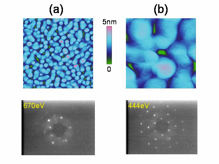
6 As a first step for the epitaxial growth, we compared RF and DC operation using the same sputtering gun. Fig. 1(a) & (b) show the difference between RF and DC sputtered films grown both at 850 C, respectively. The DC sputtered film shows better epitaxy even with a higher deposition rate than the RF sputtered film. AFM of these samples shows that the island sizes are much larger in DC sputtered films (> 100 nm in diameter) than for RF sputtered films (< 50 nm in diameter). In addition, DC sputtered films show atomic step terraces, while RF sputtered films show no terraces within the AFM resolution. Finally, the DC sputtered films show sharper hexagonal LEED patterns than the RF sputtered films. These differences are most likely due to the fact that RF sputtering has more of an etching effect on the sample surface during deposition than does DC sputtering. This observation indicates that DC operation is better for epitaxial growth. Accordingly, all the following growth studies were performed using only DC sputtering. The quality of the epitaxy is sensitive to both the sputtering power and the substrate temperature. For example, when the deposition rate was higher than 1 Å/s (DC, 30 W), no diffraction pattern was seen in LEED. In contrast, with reduced deposition rate of ~0.3 Å/s (DC, 6 W), both a sharp diffraction pattern in LEED and terraced islands in AFM
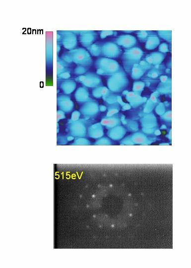
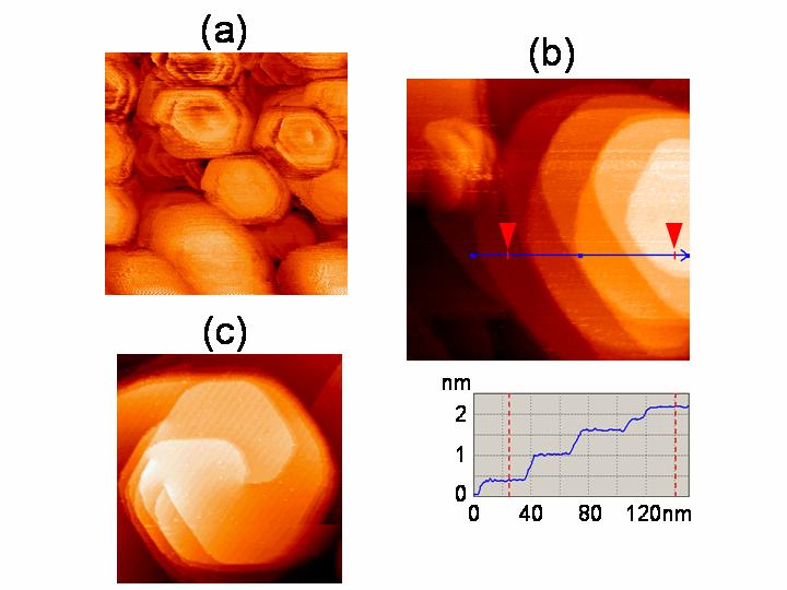
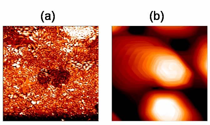
7 were observed, as shown in Fig. 1(b). However, even with the lowest deposition rate of ~0.3 Å/s, for substrate temperatures below 500 C, no measurable LEED pattern was observed. On the other hand, when the growth temperature was increased to 700 C, a noticeable diffraction pattern showed up (Fig. 2). In fact, the epitaxial quality continues to improve as the growth temperature increases, as shown for an 850 C grown film in Fig. 1(b). Comparison of both the AFM images and the LEED patterns shows that higher growth temperature is preferable for Re epitaxy. With in situ STM studies, more accurate morphological information can be obtained with minimal surface contamination problems. The STM image in Fig. 3(a) shows that an 850 C (DC, 7 W) grown film is composed of terraced, hexagonal islands that are typically ~100 nm in diameter. As shown in Fig. 3(b) the most commonly observed step is 3 Å high. This corresponds to two atomic Re layers, considering that the c-axis lattice constant of the tri-atomic layered hcp Re unit cell is ~4.5 Å. Frequently, two terraces merge into a 6 Å step and occasionally multiple steps converge to form steeper edges. Another interesting feature is that every hexagonal island has a screw dislocation at the center as shown in Fig. 3(c). This indicates that the growth proceeds in a spiral mode
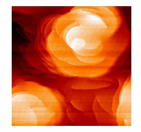
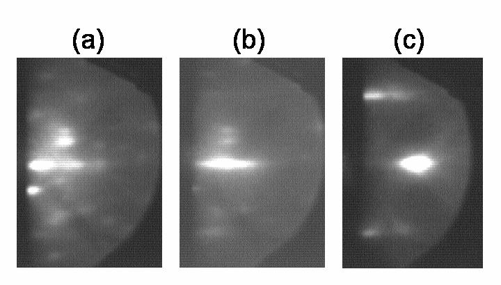
8 with the screw dislocation as the growth flow axis. This spiral growth is a well-known phenomenon [9] and is commonly observed in other systems [10-12]. When the 850 C grown film was annealed at 1200 C for half an hour, the terraces got wider and the average island diameter increased to about 200 nm, as shown in Fig. 4. However, qualitative features of the epitaxial film such as the existence of screw dislocations and multiple step terraces remain unchanged. The RHEED images in Fig. 5 show the epitaxial growth evolution at 850 C. Initially, the film grows in a 3D fashion, which appears as a multiply oriented, spotty diffraction pattern shown in Fig. 5(a). As the film gets thicker, the 3D spots gradually diminish, and 2D streaks start to develop (Fig. 5(b)). Eventually when the film gets much thicker (> 50 nm), only 2D streaks remain (Fig. 5(c)). This indicates that the initial heteroepitaxy (Re on sapphire) starts as Volmer-Weber (VW) type (3D growth) but that later the Re homoepitaxy (Re on Re) proceeds with Frank-Van der Merwe (FV) mode (2D growth) [13].
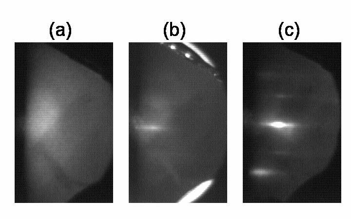
9 The initial VW 3D mode can be avoided by use of a seed layer technique [14]. When a thin (2 nm) Re is deposited at room temperature, no discernible RHEED pattern is observed (Fig. 6(a)), indicating that the film is not ordered. However, high temperature (850 C) annealing of this seed layer transforms it into a single crystalline 2D structure, which appears as a streaky RHEED pattern in Fig. 6(b). When more Re is deposited on top of the seed layer at 850 C, the RHEED remains 2D throughout the whole growth (Fig. 6(c)). The effect of this seed layer scheme is shown also in the STM images of Fig. 7(a)&(b). When the seed layer is annealed at 850 C, the film remains flat with randomly shaped small islands (Fig. 7(a)). At this stage, the surface morphology reflects the combined roughness of the substrate and the film. After another 130 nm of Re is deposited onto the seed layer at 850 C, large hexagonal islands are observed (Fig. 7(b)). Compared with the film in Fig. 3(a), which was grown without any seed layer, the most significant difference is that the islands are a factor of two larger (~200 nm vs. ~100 nm in diameters). Other than that, other features are similar. This shows that the epitaxial features such as hexagonal islands, screw dislocations and multiple steps are not due to the initial VW growth mode but are an intrinsic thermodynamic property of Re (0001) growth.
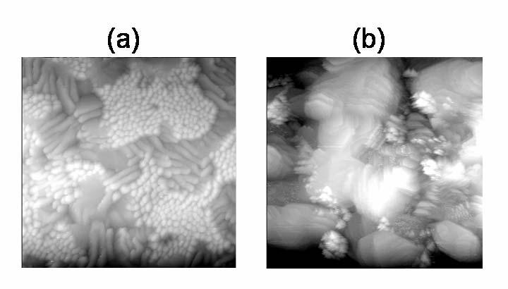
10 Finally, in order to see the effect of temperature on the surface morphology of Re, we performed annealing tests on room temperature (RT) sputtered Re films. According to RHEED (very diffuse and not shown here), a RT sputtered Re film grows polycrystalline. The STM image in Fig. 8(a) shows that the RT sputtered film (130 nm thick) is composed of small islands with c-axis normal to the surface and tubular structures with c- axis along the tube direction. When the film was heated, a major morphology transformation occurred at around 600 C, above which temperature c-axis oriented hexagonal islands emerged together with other complicated structures (Fig. 8(b)) (RHEED also showed streaky but diffuse diffraction (not shown here)). This implies that although the annealed RT grown films show some epitaxial features, they are not completely single-crystalline. Additional annealing to higher temperatures (up to 1200 C) induced no further qualitative change in the morphology. 4. Summary We described growth of epitaxial Re film on sapphire substrate with sputtering. Under similar growth conditions, DC sputtering gives noticeably better epitaxy than RF. The best epitaxy is obtained at the lowest deposition rate and at the highest growth temperature. With DC sputtering, considerable epitaxy is obtained only below 1 Å/s in
11 deposition rate and above 700 C in growth temperature. Epitaxial Re (0001) films are composed of hexagonal islands with screw dislocations and multiply stepped terraces. High temperature epitaxial growth directly onto the base sapphire surface starts with initial 3D growth mode and gradually transforms into 2D growth. A thin seed layer grown at room temperature and annealed at a high temperature helps suppress the initial 3D growth and results in island sizes larger by a factor of two. However, all of these epitaxial films showed evidence of multiple steps that appear to be converging into larger, a-plane faces that are perpendicular to the film plane. The question of whether or not these are atomically flat planes could not be resolved in this study due to the finite radius of the STM tip. We are currently investigating the efficacy of these films as the bottom electrode for tunnel junctions in superconducting quantum bit devices. Acknowledgement We appreciate useful discussions with Paul Welander, J. N. Eckstein and Alexander Popov. This work was supported by the National Security Agency (NSA) Advanced Research and Development Activity (ARDA) through Army Research Office grants W911NF and MOD717304, by the North Atlantic Treaty Organization
12 (NATO) through Grant PST.CLG , and by the National Institute of Standards and Technology (NIST).
13 References [1] R. W. Simmonds, K. M. Lang, D. A. Hite, S. Nam, D. P. Pappas and J. M. Martinis, Phys. Rev. Lett., 93 (2004) /1. [2] Y. Wu, E. Garfunkel, and T. E. Madey, J. Vac. Sci. Technol., A 14 (1996) [3] A. U. Haq and O. Meyer, Thin Solid Films, 94 (1982) 119. [4] G. V. Samsonov, The Oxide Handbook, (IFI/Plenum Data Company, 1982). [5] A. R. Wildes, J. Mayer, and K. Theis-Bröhl, Thin Solid Films, 401 (2001) 7. [6] A. Cho, Molecular Beam Epitaxy, (Woodburry, New York, 1994). [7] G. R. Harp and S. S. P. Parkin, Thin Solid Films, 288 (1996) 315. [8] T. Bauer, M. Schreck, S. Gsell, F. Hormann, and B. Stritzker, Phys. Stat. Sol. (A), 199 (2003) 19. [9] N. W. Ashcroft and N. D. Mermin, Solid State Physics, Chap 30 (W. B. Saunders Company, 1976). [10] S. H. Cheung, L. X. Zheng, M. H. Xie, S. Y. Tong and N. Ohtani, Phy. Rev. B 64, (2001) [11] B. Wassermann, Philosophical Magazine, 83 (2003) [12] P. Sobotik and I. Ošt ádal, J. of Crystal Growth, 197 (1999) 955. [13] A. Zangwill, Physics at Surfaces, Chap 16 (Cambridge University Press, 1988).
14 [14] A. R. Smith, K.-J. Chao, Q. Niu and C.-K. Shih, Science, 273 (1996) 223.
15 Figure Captions Figure 1: AFM and LEED images of RF vs DC sputtered films grown at 850 C; both are 130 nm thick. Scan area is 1 µm 1 µm. (a) RF 30 W, 0.17 Å/s. (b) DC 6 W, 0.26 Å/s. DC sputtering results in sharper LEED patterns and much larger islands even with a higher deposition rate. Figure 2: Epitaxy obtained at 700 C with DC 6 W; film thickness is 130 nm. Scan area is 1 µm 1 µm. No measurable LEED pattern is observed up to the growth temperature of 500 C. When the growth temperature is increased to 700 C, a clear diffraction pattern emerges as shown here. However, compared with the 850 C grown film presented in Fig. 1(b), the 700 C grown film has inferior epitaxial quality; the surface is rougher, island sizes are smaller, and the LEED pattern is not as sharp. Figure 3: STM images of an epitaxial film (DC 7 W, 0.35 Å/s, grown at 850 C, 130 nm thick). (a) Scan area is 500 nm 500 nm and the full gray scale corresponds to ~15 nm in height. Hexagonal islands (~100 nm in diameter) are commonly observed,
16 which is related to the c-axis oriented hcp structure. (b) Zoomed-in view of (a) (220 nm 220 nm scan area). The line scan covers two single steps and two double steps, and results in height variation of ~1.8 nm. This implies that the single step (~3.0 Å) corresponds to two Re atomic layers since the c-axis lattice constant of hcp Re, which is composed of three Re atomic layers, is ~4.5 Å. Occasionally multiple steps merge together to form steep edges. (c) Zoomed-in view of a typical hexagonal island, which has a screw dislocation at the center: 200 nm 200 nm scan area. Figure 4: STM image taken after 1200 C annealing of an 850 C grown epitaxial film (500 nm 500 nm of scan area). Compared with Fig. 3(a), the island sizes are about twice as large in diameter (~200 nm) and the terraces have also become noticeably wider. Figure 5: RHEED images at different stages of epitaxial growth (850 C, DC 7 W). (a) After 2 nm of Re, multiply oriented 3D spots are observed. (b) After 10 nm of Re, 3D spots are weaker and 2D streaks are more pronounced. (c) After 100 nm of Re, 3D spots are completely gone and only bright 2D streaks are observable.
17 Figure 6: RHEED images for the seed layer growth scheme. (a) After 2 nm of Re is sputtered at room temperature, no diffraction pattern is observed. (b) When the seed layer is annealed at 850 C, a streaky diffraction pattern shows up, which implies that the seed layer has become 2D and single-crystalline. (c) 130 nm of Re is sputtered on top of the seed layer at 850 C and a sharp 2D diffraction pattern is observed; 2D growth mode is maintained throughout the whole growth. Figure 7: STM images for the seed layer growth scheme (500 nm 500 nm of scan area). (a) After 2 nm of RT sputtered Re is annealed at 850 C, the surface is composed of tiny islands (~10 nm in diameter). The full gray scale corresponds to ~3 nm in height. (b) After 130 nm of Re is deposited on top of the seed layer at 850 C, large islands (~200 nm in diameter) with many terrace steps are formed. The full gray scale corresponds to ~15 nm in height. Note that the islands are significantly bigger than those of the regular 850 C grown films (Fig. 3(a)). Figure 8: Annealing test of RT grown films (500 nm 500 nm of scan area). The full gray scale corresponds to ~10 nm in height for both images. (a) 130 nm of Re sputtered at RT. Circular islands with c-axis normal to the surface and tubular
18 islands with c-axis along the tubular axis are observed. (b) After the RT sputtered Re film is annealed above 600 C, the surface morphology is completely changed. This particular image is obtained after 750 C annealing. Not only hexagonal islands, but also other complicated oriented features can be seen. Although not clearly shown in this image, screw dislocations are also observed on the hexagonal islands.
19 Figure 1
20 Figure 2
21 Figure 3
22 Figure 4
23 Figure 5
24 Figure 6
25 Figure 7
26 Figure 8
Nucleation and growth of nanostructures and films. Seongshik (Sean) Oh
 Oh") Nucleation and growth of nanostructures and films Seongshik (Sean) Oh Outline Introduction and Overview 1. Thermodynamics and Kinetics of thin film growth 2. Defects in films 3. Amorphous, Polycrystalline
Nucleation and growth of nanostructures and films Seongshik (Sean) Oh Outline Introduction and Overview 1. Thermodynamics and Kinetics of thin film growth 2. Defects in films 3. Amorphous, Polycrystalline
Epitaxial growth of (001) and (111) Ni films on MgO substrates
 and (111) Ni films on MgO substrates") Epitaxial growth of (001) and (111) Ni films on MgO substrates Rosa Alejandra Lukaszew 1, Vladimir Stoica, Ctirad Uher and Roy Clarke Physics Department, University of Michigan, Ann Arbor 1 Presently at
Epitaxial growth of (001) and (111) Ni films on MgO substrates Rosa Alejandra Lukaszew 1, Vladimir Stoica, Ctirad Uher and Roy Clarke Physics Department, University of Michigan, Ann Arbor 1 Presently at
Scanning tunneling microscopy observation of surface reconstruction of GaN on sapphire and 6H-SiC
 Scanning tunneling microscopy observation of surface reconstruction of GaN on sapphire and 6H-SiC A.R. Smith*, V. Ramachandran*, R.M. Feenstra*, D.W. Greve**, J. Neugebauer***, J.E. Northrup****, M. Shin*****,
Temperature dependence of molecular beam epitaxy of GaN on SiC (0001)
") Temperature dependence of molecular beam epitaxy of GaN on SiC (0001) V. Ramachandran a, A. R. Smith a, R. M. Feenstra a and D. W. Greve b a Department of Physics, b Department of Electrical and Computer
Temperature dependence of molecular beam epitaxy of GaN on SiC (0001) V. Ramachandran a, A. R. Smith a, R. M. Feenstra a and D. W. Greve b a Department of Physics, b Department of Electrical and Computer
6.8 Magnetic in-plane anisotropy of epitaxially grown Fe-films on vicinal Ag(001) and Au(001) with different miscut orientations
 and Au(001) with different miscut orientations") C. Epitaxial Growth 6.8 Magnetic in-plane anisotropy of epitaxially grown Fe-films on vicinal Ag(001) and Au(001) with different miscut orientations M. Rickart, A.R. Frank, J. Jorzick, Ch. Krämer, S.O.
C. Epitaxial Growth 6.8 Magnetic in-plane anisotropy of epitaxially grown Fe-films on vicinal Ag(001) and Au(001) with different miscut orientations M. Rickart, A.R. Frank, J. Jorzick, Ch. Krämer, S.O.
Morphology of Thin Aluminum Film Grown by DC Magnetron Sputtering onto SiO 2 on Si(100) Substrate
 Substrate") Morphology of Thin Aluminum Film Grown by DC Magnetron Sputtering onto SiO 2 on Si(1) Substrate Fan Wu Microelectronics Center, Medtronic Inc., Tempe, AZ 85261 James E. Morris Department of Electrical
Morphology of Thin Aluminum Film Grown by DC Magnetron Sputtering onto SiO 2 on Si(1) Substrate Fan Wu Microelectronics Center, Medtronic Inc., Tempe, AZ 85261 James E. Morris Department of Electrical
Deposition and characterization of sputtered ZnO films
 Superlattices and Microstructures 42 (2007) 89 93 www.elsevier.com/locate/superlattices Deposition and characterization of sputtered ZnO films W.L. Dang, Y.Q. Fu, J.K. Luo, A.J. Flewitt, W.I. Milne Electrical
Molecular Beam Epitaxy (MBE) BY A.AKSHAYKRANTH JNTUH
 BY A.AKSHAYKRANTH JNTUH") Molecular Beam Epitaxy (MBE) BY A.AKSHAYKRANTH JNTUH CONTENTS Introduction What is Epitaxy? Epitaxy Techniques Working Principle of MBE MBE process & Epitaxial growth Working conditions Operation Control
Molecular Beam Epitaxy (MBE) BY A.AKSHAYKRANTH JNTUH CONTENTS Introduction What is Epitaxy? Epitaxy Techniques Working Principle of MBE MBE process & Epitaxial growth Working conditions Operation Control
OUTLINE. Preparation of III Nitride thin 6/10/2010
 Preparation of III Nitride thin films for LEDs Huaxiang Shen Supervisor: Dr. Adrian Kitai 1 2 Two kinds of EL devices Light emitting diodes Powder EL and thin film EL http://en.wikipedia.org/wiki/file:pnjunction
TEM Study of the Morphology Of GaN/SiC (0001) Grown at Various Temperatures by MBE
 Grown at Various Temperatures by MBE") TEM Study of the Morphology Of GaN/SiC (0001) Grown at Various Temperatures by MBE W.L. Sarney 1, L. Salamanca-Riba 1, V. Ramachandran 2, R.M Feenstra 2, D.W. Greve 3 1 Dept. of Materials & Nuclear Engineering,
TEM Study of the Morphology Of GaN/SiC (0001) Grown at Various Temperatures by MBE W.L. Sarney 1, L. Salamanca-Riba 1, V. Ramachandran 2, R.M Feenstra 2, D.W. Greve 3 1 Dept. of Materials & Nuclear Engineering,
Growth and Surface Reconstructions of AlN(0001) Films
 Films") Growth and Surface Reconstructions of AlN(0001) Films C. D. Lee 1*, Y. Dong 1, R. M. Feenstra 1, J. E. Northrup 2, J. Neugebauer 3 1 Dept. Physics, Carnegie Mellon University, Pittsburgh, PA 15213 2 Palo
Growth and Surface Reconstructions of AlN(0001) Films C. D. Lee 1*, Y. Dong 1, R. M. Feenstra 1, J. E. Northrup 2, J. Neugebauer 3 1 Dept. Physics, Carnegie Mellon University, Pittsburgh, PA 15213 2 Palo
Effect of substrate heating on elimination of pinholes in sputtering deposited SiO2 films on LiNbO3 single crystal substrates
 Thin Solid Films 335 (1998) 117-121 Effect of substrate heating on elimination of pinholes in sputtering deposited SiO2 films on LiNbO3 single crystal substrates Hirotoshi Nagata a, *, Tetsuya Fujino b,
Preparation of atomically clean and flat Si(100) surfaces by low-energy ion sputtering and low-temperature annealing
 surfaces by low-energy ion sputtering and low-temperature annealing") Preparation of atomically clean and flat Si(100) surfaces by low-energy ion sputtering and low-temperature annealing J. C. Kim a,b, J.-Y. Ji b, J. S. Kline a, J. R. Tucker a, and T.-C. Shen b,* a Department
Preparation of atomically clean and flat Si(100) surfaces by low-energy ion sputtering and low-temperature annealing J. C. Kim a,b, J.-Y. Ji b, J. S. Kline a, J. R. Tucker a, and T.-C. Shen b,* a Department
8. Epitaxy. - Extended single-crystal film formation on top of a crystalline substrate
 8. Epitaxy 1. Introduction επι(epi placed or resting upon) ταξιζ(taxis arrangement) - Extended single-crystal film formation on top of a crystalline substrate - Homoepitaxy : Film and substrate are the
Evolution of atomic-scale roughening on Si(001)-(2 1) surfaces resulting from high temperature oxidation
-(2 1) surfaces resulting from high temperature oxidation") Evolution of atomic-scale roughening on Si(001)-(2 1) surfaces resulting from high temperature oxidation J. V. Seiple and J. P. Pelz Department of Physics, The Ohio State University, Columbus, Ohio 43210
Evolution of atomic-scale roughening on Si(001)-(2 1) surfaces resulting from high temperature oxidation J. V. Seiple and J. P. Pelz Department of Physics, The Ohio State University, Columbus, Ohio 43210
Applications for HFETs
 Applications for HFETs Ga-face Quantum well is formed at the interface AlGaN GaN Buffer P SP P SP P PE -σ s +σ int 2DEG + ve φ b d σ comp AlGaN σ int E 0 GaN E c E F c-plane sapphire σ 2DEG σ surf Higher
Supporting Online Material for
 www.sciencemag.org/cgi/content/full/327/5961/60/dc1 Supporting Online Material for Polarization-Induced Hole Doping in Wide Band-Gap Uniaxial Semiconductor Heterostructures John Simon, Vladimir Protasenko,
Ruthenium Oxide Films Prepared by Reactive Biased Target Sputtering
 Ruthenium Oxide Films Prepared by Reactive Biased Target Sputtering Hengda Zhang Anthony Githinji 1. Background RuO2 in both crystalline and amorphous forms is of crucial importance for theoretical as
Physics and Material Science of Semiconductor Nanostructures
 Physics and Material Science of Semiconductor Nanostructures PHYS 570P Prof. Oana Malis Email: omalis@purdue.edu Today Bulk semiconductor growth Single crystal techniques Nanostructure fabrication Epitaxial
ARTICLE IN PRESS. Materials Science in Semiconductor Processing
 Materials Science in Semiconductor Processing ] (]]]]) ]]] ]]] Contents lists available at ScienceDirect Materials Science in Semiconductor Processing journal homepage: www.elsevier.com/locate/mssp High-dielectric
Annealing effects on (0 0 1) Ni films grown on MgO
 Ni films grown on MgO") Applied Surface Science 219 (2003) 74 79 Annealing effects on (0 0 1) Ni films grown on MgO Rosa Alejandra Lukaszew a,*, Zhengdong Zhang a, Vladimir Stoica b, Roy Clarke b a Department of Physics and Astronomy,
Applied Surface Science 219 (2003) 74 79 Annealing effects on (0 0 1) Ni films grown on MgO Rosa Alejandra Lukaszew a,*, Zhengdong Zhang a, Vladimir Stoica b, Roy Clarke b a Department of Physics and Astronomy,
High Density Iron Silicide Nanodots Formed by Ultrathin SiO 2 Film Technique
 Available online at www.sciencedirect.com Procedia Engineering 36 (2012 ) 382 387 IUMRS-ICA 2011 High Density Iron Silicide Nanodots Formed by Ultrathin SiO 2 Film Technique Yoshiaki Nakamura a,b* a Graduate
Heterostructures of Oxides and Semiconductors - Growth and Structural Studies
 Heterostructures of Oxides and Semiconductors - Growth and Structural Studies Beamline 17B1 W20 X-ray Scattering beamline Authors M. Hong and J. R. Kwo National Tsing Hua University, Hsinchu, Taiwan H.
Croissance et propriétés magnétiques de réseaux planaires auto-organisés de nanofils de Fer
 Croissance et propriétés magnétiques de réseaux planaires auto-organisés de nanofils de Fer B. Borca, O.Fruchart, M. Hasegawa, C. Meyer Laboratoire Louis Néel (CNRS-UJF-INPG) Grenoble Olivier Fruchart
SiC crystal growth from vapor
 SiC crystal growth from vapor Because SiC dissolves in Si and other metals can be grown from melt-solutions: Liquid phase epitaxy (LPE) Solubility of C in liquid Si is 0.029% at 1700oC high T process;
The Fabrication of Epitaxial Magnetic Tunnel Junctions. Drew Allen, Rainer Schad
 The Fabrication of Epitaxial Magnetic Tunnel Junctions Drew Allen, Rainer Schad and Department of Physics and Astronomy University of Alabama Why Epitaxial Tunnel Junctions? Magnetic Tunnel junctions consist
Simple method for formation of nanometer scale holes in membranes. E. O. Lawrence Berkeley National Laboratory, Berkeley, CA 94720
 Simple method for formation of nanometer scale holes in membranes T. Schenkel 1, E. A. Stach, V. Radmilovic, S.-J. Park, and A. Persaud E. O. Lawrence Berkeley National Laboratory, Berkeley, CA 94720 When
Structural Properties of GaN Films Grown by Molecular Beam Epitaxy on Singular and Vicinal 6H-SiC(0001)
") Structural Properties of GaN Films Grown by Molecular Beam Epitaxy on Singular and Vicinal 6H-SiC(0001) C. D. Lee, 1 R. M. Feenstra, 1 O. Shigiltchoff, 2 R. P. Devaty 2 and W. J. Choyke 2 1 Department
Structural Properties of GaN Films Grown by Molecular Beam Epitaxy on Singular and Vicinal 6H-SiC(0001) C. D. Lee, 1 R. M. Feenstra, 1 O. Shigiltchoff, 2 R. P. Devaty 2 and W. J. Choyke 2 1 Department
Magnetic Tunnel Junction Based on MgO Barrier Prepared by Natural Oxidation and Direct Sputtering Deposition
 www.nmletters.org Magnetic Tunnel Junction Based on MgO Barrier Prepared by Natural Oxidation and Direct Sputtering Deposition Xiaohong Chen 1,2,, Paulo. P. Freitas 2 (Received 12 December 11; accepted
Growth and Doping of SiC-Thin Films on Low-Stress, Amorphous Si 3 N 4 /Si Substrates for Robust Microelectromechanical Systems Applications
 Journal of ELECTRONIC MATERIALS, Vol. 31, No. 5, 2002 Special Issue Paper Growth and Doping of SiC-Thin Films on Low-Stress, Amorphous Si 3 N 4 /Si Substrates for Robust Microelectromechanical Systems
Growth Of TiO 2 Films By RF Magnetron Sputtering Studies On The Structural And Optical Properties
 Journal of Multidisciplinary Engineering Science and Technology (JMEST) Growth Of TiO 2 Films By RF Magnetron Sputtering Studies On The Structural And Optical Properties Ahmed K. Abbas 1, Mohammed K. Khalaf
Pre-treatment of low temperature GaN buffer layer deposited on AlN Si substrate by hydride vapor phase epitaxy
 Ž. Surface and Coatings Technology 131 000 465 469 Pre-treatment of low temperature GaN buffer layer deposited on AlN Si substrate by hydride vapor phase epitaxy Ha Jin Kim, Ho-Sun Paek, Ji-Beom Yoo Department
Preparation and characterization of Co BaTiO 3 nano-composite films by the pulsed laser deposition
 Journal of Crystal Growth 289 (26) 48 413 www.elsevier.com/locate/jcrysgro Preparation and characterization of Co BaTiO 3 nano-composite films by the pulsed laser deposition Wu Weidong a,b,, He Yingjie
Ferromagnetic transition in Ge 1 x Mn x Te semiconductor layers
 Materials Science-Poland, Vol. 25, No. 2, 2007 Ferromagnetic transition in Ge 1 x Mn x Te semiconductor layers W. KNOFF *, P. DZIAWA, V. OSINNIY, B. TALIASHVILI, V. DOMUCHOWSKI, E. ŁUSAKOWSKA, K. ŚWIĄTEK,
Thermal Evaporation. Theory
 Thermal Evaporation Theory 1. Introduction Procedures for depositing films are a very important set of processes since all of the layers above the surface of the wafer must be deposited. We can classify
Synthesis and Characterization of DC Magnetron Sputtered ZnO Thin Films Under High Working Pressures
 Accepted Manuscript Synthesis and Characterization of DC Magnetron Sputtered ZnO Thin Films Under High Working Pressures M. Hezam, N. Tabet, A. Mekki PII: S0040-6090(10)00417-7 DOI: doi: 10.1016/j.tsf.2010.03.091
Preparation and structural characterization of thin-film CdTe/CdS heterojunctions
 JOURNAL OF OPTOELECTRONICS AND ADVANCED MATERIALS Vol. 8, No., June 006, p. 96-940 Preparation and structural characterization of thin-film CdTe/ heterojunctions I. SALAORU a, P. A. BUFFAT b, D. LAUB b,
ECE 440 Lecture 27 : Equilibrium P-N Junctions I Class Outline:
 ECE 440 Lecture 27 : Equilibrium P-N Junctions I Class Outline: Fabrication of p-n junctions Contact Potential Things you should know when you leave Key Questions What are the necessary steps to fabricate
The effect of growth parameters on CrN thin films grown by molecular beam epitaxy
 The effect of growth parameters on CrN thin films grown by molecular beam epitaxy Y. H. Liu 1, Kangkang Wang, Wenzhi Lin, Abhijit Chinchore, Meng Shi, Jeongihm Pak and A. R. Smith 1 Department of Physics
Platypus Gold Coated Substrates. Bringing Science to the Surface
 Platypus Gold Coated Substrates Bringing Science to the Surface Overview Gold Coated Substrates - Gold Coating Introduction - Glossary of Terms - Gold Coating Methods - Critical Features Platypus Gold
High-resolution electron microscopy of grain boundary structures in yttria-stabilized cubic zirconia
 Mat. Res. Soc. Symp. Proc. Vol. 654 2001 Materials Research Society High-resolution electron microscopy of grain boundary structures in yttria-stabilized cubic zirconia K. L. Merkle, L. J. Thompson, G.-R.
Institute of Solid State Physics. Technische Universität Graz. Deposition. Franssila: Chapters 5 & 6. Peter Hadley
 Technische Universität Graz Institute of Solid State Physics Deposition Franssila: Chapters 5 & 6 Peter Hadley Silicon wafers Total Thickness Variation: a good 8" Prime wafer would be < 15 m Site flatness
Optimized structural properties of wurtzite GaN on SiC(0001) grown by molecular beam epitaxy
 grown by molecular beam epitaxy") Optimized structural properties of wurtzite GaN on SiC(0001) grown by molecular beam epitaxy V. Ramachandran and R. M. Feenstra Department of Physics, Carnegie Mellon University, Pittsburgh, PA 15213 W.
Optimized structural properties of wurtzite GaN on SiC(0001) grown by molecular beam epitaxy V. Ramachandran and R. M. Feenstra Department of Physics, Carnegie Mellon University, Pittsburgh, PA 15213 W.
Delta-phase manganese gallium on gallium nitride: a magnetically tunable spintronic system
 Mater. Res. Soc. Symp. Proc. Vol. 1118 2009 Materials Research Society 1118-K06-06 Delta-phase manganese gallium on gallium nitride: a magnetically tunable spintronic system Kangkang Wang 1, Abhijit Chinchore
Citation for published version (APA): Borsa, D. M. (2004). Nitride-based insulating and magnetic thin films and multilayers s.n.
: Borsa, D. M. (2004). Nitride-based insulating and magnetic thin films and multilayers s.n.") University of Groningen Nitride-based insulating and magnetic thin films and multilayers Borsa, Dana Maria IMPORTANT NOTE: You are advised to consult the publisher's version (publisher's PDF) if you wish
University of Groningen Nitride-based insulating and magnetic thin films and multilayers Borsa, Dana Maria IMPORTANT NOTE: You are advised to consult the publisher's version (publisher's PDF) if you wish
Formation of Cupric Oxide Films on Quartz Substrates by Annealing the Copper Films
 Journal of Applied Chemical Research, 9, 2, 73-79 (2015) Journal of Applied Chemical Research www.jacr.kiau.ac.ir Formation of Cupric Oxide Films on Quartz Substrates by Annealing the Copper Films Abstract
Pulsed Laser Deposition of Epitaxial Titanium Nitride on Magnesium Oxide substrate
 Pulsed Laser Deposition of Epitaxial Titanium Nitride on Magnesium Oxide substrate By, Preetam ANBUKARASU UTRIP 2012 (1 st Crew) Under the Guidance of, Prof. Tetsuya HASEGAWA, Solid State Chemistry Lab,
Ag 2 S: Fabrication and Characterization Techniques
 2 2 S: Fabrication and Characterization Techniques This chapter describes two fabrication methods used for the growth of 2 S thin films. The specific growth parameters are presented for each method as
InGaAs (110) surface cleaning using atomic hydrogen Tyler Kent 1, Mary Edmonds 1, Ravi Droopad 3, Andrew C. Kummel 1,2,a
 surface cleaning using atomic hydrogen Tyler Kent 1, Mary Edmonds 1, Ravi Droopad 3, Andrew C. Kummel 1,2,a") Solid State Phenomena Vol. 219 (2015) pp 47-51 Online available since 2014/Sep/26 at www.scientific.net (2015) Trans Tech Publications, Switzerland doi:10.4028/www.scientific.net/ssp.219.47 InGaAs (110)
Solid State Phenomena Vol. 219 (2015) pp 47-51 Online available since 2014/Sep/26 at www.scientific.net (2015) Trans Tech Publications, Switzerland doi:10.4028/www.scientific.net/ssp.219.47 InGaAs (110)
Silver Diffusion Bonding and Layer Transfer of Lithium Niobate to Silicon
 Chapter 5 Silver Diffusion Bonding and Layer Transfer of Lithium Niobate to Silicon 5.1 Introduction In this chapter, we discuss a method of metallic bonding between two deposited silver layers. A diffusion
III Fabrication of the samples
 III Fabrication of the samples The fabrication of the samples for SPR measurement consists of three steps. It begins with glass substrates cleaning using ultrasonication, followed by the deposition of
Development of low roughness, low resistance bottom electrodes for tunnel junction devices
 Development of low roughness, low resistance bottom electrodes for tunnel junction devices Designing and assembly of a new annealing setup for 150mm wafers David Filipe Coelho de Almeida Aurélio Setembro
Previous Lecture. Vacuum & Plasma systems for. Dry etching
 Previous Lecture Vacuum & Plasma systems for Dry etching Lecture 9: Evaporation & sputtering Objectives From this evaporation lecture you will learn: Evaporator system layout & parts Vapor pressure Crucible
The effect of ion milling on the morphology of ramp-type Josephson junctions
 Journal of MATERIALS RESEARCH Welcome Comments Help The effect of ion milling on the morphology of ramp-type Josephson junctions Dave H. A. Blank and Horst Rogalla Low Temperature Division, Department
CHAPTER 4. SYNTHESIS OF ALUMINIUM SELENIDE (Al 2 Se 3 ) NANO PARTICLES, DEPOSITION AND CHARACTERIZATION
 NANO PARTICLES, DEPOSITION AND CHARACTERIZATION") 40 CHAPTER 4 SYNTHESIS OF ALUMINIUM SELENIDE (Al 2 Se 3 ) NANO PARTICLES, DEPOSITION AND CHARACTERIZATION 4.1 INTRODUCTION Aluminium selenide is the chemical compound Al 2 Se 3 and has been used as a precursor
40 CHAPTER 4 SYNTHESIS OF ALUMINIUM SELENIDE (Al 2 Se 3 ) NANO PARTICLES, DEPOSITION AND CHARACTERIZATION 4.1 INTRODUCTION Aluminium selenide is the chemical compound Al 2 Se 3 and has been used as a precursor
CONDENSED MATTER. between the Ce'(111) and V(110) planes is unlike any previously observed relationship between fcc and bcc materials.
 and V(110) planes is unlike any previously observed relationship between fcc and bcc materials.") CONDENSED MATTER THIRD SERIES, VOLUME 36, NUMBER 18 15 DECEMBER 1987-II Role of lattice matching in epitaxy: Novel Ce phase and new fcc-bcc epitaxial relationship Hitoshi Homma, Kai-Y. Yang, and Ivan K.
CONDENSED MATTER THIRD SERIES, VOLUME 36, NUMBER 18 15 DECEMBER 1987-II Role of lattice matching in epitaxy: Novel Ce phase and new fcc-bcc epitaxial relationship Hitoshi Homma, Kai-Y. Yang, and Ivan K.
Citation for published version (APA): Borsa, D. M. (2004). Nitride-based insulating and magnetic thin films and multilayers s.n.
: Borsa, D. M. (2004). Nitride-based insulating and magnetic thin films and multilayers s.n.") University of Groningen Nitride-based insulating and magnetic thin films and multilayers Borsa, Dana Maria IMPORTANT NOTE: You are advised to consult the publisher's version (publisher's PDF) if you wish
University of Groningen Nitride-based insulating and magnetic thin films and multilayers Borsa, Dana Maria IMPORTANT NOTE: You are advised to consult the publisher's version (publisher's PDF) if you wish
SiC high voltage device development
 SiC high voltage device development 2006. 11. 30 KERI Power Semiconductor Group outline 1. Device design & simulation for power devices 2. SiC power diode process development Ion implantation & activation
Growth of aluminum oxide thin lms on Cobalt : an AES and AFM study
 J. Phys. IV France 1 (2005) Pr1-1 c EDP Sciences, Les Ulis Growth of aluminum oxide thin lms on Cobalt : an AES and AFM study =0by 1 H. Oughaddou 1;, S. Vizzini 1 ; B. Aufray 1, B. Ealet 1, L. Ravel 1,
Epitaxy and Roughness Study of Glancing Angle Deposited Nanoarrays. Hamid Alouach and G. J. Mankey
 Epitaxy and Roughness Study of Glancing Angle Deposited Nanoarrays Hamid Alouach and G. J. Mankey Introduction Objective: Approach: Characterization: Fabrication of nanoscale magnetic wires for spin transport
Low Thermal Budget NiSi Films on SiGe Alloys
 Mat. Res. Soc. Symp. Proc. Vol. 745 2003 Materials Research Society N6.6.1 Low Thermal Budget NiSi Films on SiGe Alloys S. K. Ray 1,T.N.Adam,G.S.Kar 1,C.P.SwannandJ.Kolodzey Department of Electrical and
Epitaxy is the deposition of layers, which are monocrystalline in large regions
 Repetition: Epitaxy Epitaxy is the deposition of layers, which are monocrystalline in large regions Homoepitaxy: Substrate material = film material Heteroepitaxy: Substrate material film material Repetition:
Deposition of TiN/CrN hard superlattices by reactive d.c. magnetron sputtering
 Bull. Mater. Sci., Vol. 26, No. 2, February 2003, pp. 233 237. Indian Academy of Sciences. Deposition of TiN/CrN hard superlattices by reactive d.c. magnetron sputtering HARISH C BARSHILIA and K S RAJAM*
Influence of the oxide thickness on the magnetic properties of Fe/ FeO multilayers.
 DESY Summer Student Program Influence of the oxide thickness on the magnetic properties of Fe/ FeO multilayers. Student: Guryeva Tatyana Supervisors: Ralf Röhlsberger Kai Schlage Sebastien Couet Hamburg,
Self-assembly of iron nanoclusters on the Fe 3 O 4 (111) superstructured surface
 superstructured surface") Self-assembly of iron nanoclusters on the Fe 3 O 4 (111) superstructured surface N. Berdunov, G. Mariotto, S. Murphy,.V. Shvets SF Laboratories, Physics Dept., Trinity College, Dublin, reland Abstract
Self-assembly of iron nanoclusters on the Fe 3 O 4 (111) superstructured surface N. Berdunov, G. Mariotto, S. Murphy,.V. Shvets SF Laboratories, Physics Dept., Trinity College, Dublin, reland Abstract
Next Generation High-Efficiency Low-cost Thin Film Photovoltaics
 Next Generation High-Efficiency Low-cost Thin Film Photovoltaics Investigators Bruce Clemens, Professor, Materials Science and Engineering, Stanford University, Alberto Salleo, Assistant Professor, Materials
arxiv:cond-mat/ v2 [cond-mat.mtrl-sci] 29 Nov 2003
![arxiv:cond-mat/ v2 [cond-mat.mtrl-sci] 29 Nov 2003](/thumbs/93/114120274.jpg "arxiv:cond-mat/ v2 [cond-mat.mtrl-sci] 29 Nov 2003") Fabrication and Electrical Properties of Pure Phase Films B. G. Chae, D. H. Youn, H. T. Kim, S. Maeng, and K. Y. Kang Basic Research Laboratory, ETRI, Daejeon 305-350, Republic of Korea arxiv:cond-mat/0311616v2
Fabrication and Electrical Properties of Pure Phase Films B. G. Chae, D. H. Youn, H. T. Kim, S. Maeng, and K. Y. Kang Basic Research Laboratory, ETRI, Daejeon 305-350, Republic of Korea arxiv:cond-mat/0311616v2
PARAMETER EFFECTS FOR THE GROWTH OF THIN POROUS ANODIC ALUMINUM OXIDES
 10.1149/1.2794473, The Electrochemical Society PARAMETER EFFECTS FOR THE GROWTH OF THIN POROUS ANODIC ALUMINUM OXIDES S. Yim a, C. Bonhôte b, J. Lille b, and T. Wu b a Dept. of Chem. and Mat. Engr., San
Effects of annealing time on defect-controlled ferromagnetism in Ga 1-x Mn x As
 Effects of annealing time on defect-controlled ferromagnetism in Ga 1-x Mn x As S. J. Potashnik, K. C. Ku, S. H. Chun, J. J. Berry, N. Samarth, and P. Schiffer* Department of Physics and Materials Research
Bulk crystal growth. A reduction in Lg will increase g m and f oper but with some costs
 Bulk crystal growth The progress of solid state device technology has depended not only on the development of device concepts but also on the improvement of materials. A reduction in Lg will increase g
CHAPTER 4 THE STUDIES OF THE CVD GROWTH PROCESS FOR EPITAXIAL DIAMOND (100) FILMS USING UHV STM
 FILMS USING UHV STM") CHAPTER 4 THE STUDIES OF THE CVD GROWTH PROCESS FOR EPITAXIAL DIAMOND (100) FILMS USING UHV STM 4.1 Introduction This chapter presents studies of the CVD diamond growth process using UHV STM. It has been
CHAPTER 4 THE STUDIES OF THE CVD GROWTH PROCESS FOR EPITAXIAL DIAMOND (100) FILMS USING UHV STM 4.1 Introduction This chapter presents studies of the CVD diamond growth process using UHV STM. It has been
Microstructure, morphology and their annealing behaviors of alumina films synthesized by ion beam assisted deposition
 Nuclear Instruments and Methods in Physics Research B 206 (2003) 357 361 www.elsevier.com/locate/nimb Microstructure, morphology and their annealing behaviors of alumina films synthesized by ion beam assisted
Synthesis of nanoscale CN x /TiAlN multilayered coatings by ion-beam-assisted deposition
 Synthesis of nanoscale / multilayered coatings by ion-beam-assisted deposition M. Cao, D. J. Li, a and X. Y. Deng College of Physics and Electronic Information Science, Tianjin Normal University, Tianjin
Optically thin palladium films on silicon-based substrates and nanostructure formation: effects of hydrogen
 Ž. Applied Surface Science 161 2000 54 60 www.elsevier.nlrlocaterapsusc Optically thin palladium films on silicon-based substrates and nanostructure formation: effects of hydrogen Andreas Othonos a,),
RightCopyright 2006 American Vacuum Soci
 Title Gallium nitride thin films deposite magnetron sputtering Author(s) Maruyama, T; Miyake, H Citation JOURNAL OF VACUUM SCIENCE & (2006), 24(4): 1096-1099 TECHNOL Issue Date 2006 URL http://hdl.handle.net/2433/43541
Lecture Day 2 Deposition
 Deposition Lecture Day 2 Deposition PVD - Physical Vapor Deposition E-beam Evaporation Thermal Evaporation (wire feed vs boat) Sputtering CVD - Chemical Vapor Deposition PECVD LPCVD MVD ALD MBE Plating
Specimen Preparation Technique for a Microstructure Analysis Using the Focused Ion Beam Process
 Specimen Preparation Technique for a Microstructure Analysis Using the Focused Ion Beam Process by Kozue Yabusaki * and Hirokazu Sasaki * In recent years the FIB technique has been widely used for specimen
Ultrathin Metal Films
 Matthias Wuttig Xiangdong Liu Ultrathin Metal Films Magnetic and Structural Properties With 234 Figures 4u Springer Contents 1 Introduction 1 References 4 2 Growth of Ultrathin Metal Films 5 2.1 Growth
TEM imaging and diffraction examples
 TEM imaging and diffraction examples Duncan Alexander EPFL-CIME 1 Diffraction examples Kikuchi diffraction Epitaxial relationships Polycrystalline samples Amorphous materials Contents Convergent beam electron
Formation mechanism of new corrosion resistance magnesium thin films by PVD method
 Surface and Coatings Technology 169 170 (2003) 670 674 Formation mechanism of new corrosion resistance magnesium thin films by PVD method a, a a a b M.H. Lee *, I.Y. Bae, K.J. Kim, K.M. Moon, T. Oki a
RHEED STUDY OF Au/KCl SYSTEM FOR ESTIMATION OF THE DEPENDENCE OF DIFFRACTION SPOT PROFILES ON THE PARTICLE SIZE
 ISSN 1330 0008 CODEN FIZAE4 RHEED STUDY OF Au/KCl SYSTEM FOR ESTIMATION OF THE DEPENDENCE OF DIFFRACTION SPOT PROFILES ON THE PARTICLE SIZE KAREL MAŠEK, VÁCLAV NEHASIL and VLADIMÍR MATOLÍN Department of
Microstructure of low temperature grown AlN thin films on Si 111
 JOURNAL OF APPLIED PHYSICS VOLUME 85, NUMBER 11 1 JUNE 1999 Microstructure of low temperature grown AlN thin films on Si 111 G. W. Auner a) and F. Jin Electrical and Computer Engineering Department, Wayne
This journal is The Royal Society of Chemistry S 1
 2013 S 1 Thermochemical analysis on the growth of NiAl 2 O 4 rods Sang Sub Kim, a Yong Jung Kwon, b Gunju Sun, a Hyoun Woo Kim,* b and Ping Wu* c a Department of Materials Science and Engineering, Inha
SUPPLEMENTARY INFORMATIONS
 SUPPLEMENTARY INFORMATIONS Dynamic Evolution of Conducting Nanofilament in Resistive Switching Memories Jui-Yuan Chen, Cheng-Lun Hsin,,, Chun-Wei Huang, Chung-Hua Chiu, Yu-Ting Huang, Su-Jien Lin, Wen-Wei
The influence of the internal microstructure on the surface parameters of polycrystalline thin films
 The influence of the internal microstructure on the surface parameters of polycrystalline thin films C. Eisenmenger-Sittner and A. Bergauer Institut für Angewandte und Technische Physik, Technische Universität
What is a positron moderator?
 What is a positron moderator? The advent of slow positron beams has resulted in nondestructive depth profiling of defects in surfaces and interfaces, low energy positron diffraction and positron remission
High-temperature induced nano-crystal formation in ion beam-induced amorphous silicon ripples
 Original Paper phys. stat. sol. (a) 204 No. 8, 2555 2560 (2007) / DOI 10.1002/pssa.200675655 High-temperature induced nano-crystal formation in ion beam-induced amorphous silicon ripples J. Grenzer *,
SUPPLEMENTARY INFORMATION
 High Electrochemical Activity of the Oxide Phase in Model Ceria- and Ceria-Ni Composite Anodes William C. Chueh 1,, Yong Hao, WooChul Jung, Sossina M. Haile Materials Science, California Institute of Technology,
In-Situ Low-Angle Cross Sectioning: Bevel Slope Flattening due to Self-Alignment Effects
 In-Situ Low-Angle Cross Sectioning: Bevel Slope Flattening due to Self-Alignment Effects UWE SCHEITHAUER SIEMENS AG, CT MM 7, Otto-Hahn-Ring 6, 81739 München, Germany Phone: + 49 89 636 44143 E-mail: uwe.scheithauer@siemens.com
The Effect of Interfacial Roughness on the Electrical Properties of Organic Thin Film Transistors with Anisotropic Dielectric Layer
 Mol. Cryst. Liq. Cryst., Vol. 476, pp. 157=[403] 163=[409], 2007 Copyright # Taylor & Francis Group, LLC ISSN: 1542-1406 print=1563-5287 online DOI: 10.1080/15421400701735673 The Effect of Interfacial
Integrated Silicon Heater for Tip-Based. Nanomanufacturing
 Supporting Information Wear Resistant Diamond Nanoprobe Tips with Integrated Silicon Heater for Tip-Based Nanomanufacturing Patrick C. Fletcher 1, Jonathan R. Felts 1, Zhenting Dai 1, Tevis T.B. Jacobs
Growth of ZnSe on GaAs(1 1 0) surfaces by molecular beam epitaxy
 surfaces by molecular beam epitaxy") Journal of Crystal Growth 186 (1998) 528 534 Growth of ZnSe on GaAs(1 1 0) surfaces by molecular beam epitaxy K.W. Koh *, M.W. Cho, Z. Zhu, T. Hanada, K.H. Yoo, M. Isshiki, T. Yao Institute for Materials
Journal of Crystal Growth 186 (1998) 528 534 Growth of ZnSe on GaAs(1 1 0) surfaces by molecular beam epitaxy K.W. Koh *, M.W. Cho, Z. Zhu, T. Hanada, K.H. Yoo, M. Isshiki, T. Yao Institute for Materials
Characterization of Nanoscale Electrolytes for Solid Oxide Fuel Cell Membranes
 Characterization of Nanoscale Electrolytes for Solid Oxide Fuel Cell Membranes Cynthia N. Ginestra 1 Michael Shandalov 1 Ann F. Marshall 1 Changhyun Ko 2 Shriram Ramanathan 2 Paul C. McIntyre 1 1 Department
Ceramic Processing Research
 Journal of Ceramic Processing Research. Vol. 11, No. 1, pp. 100~106 (2010) J O U R N A L O F Ceramic Processing Research Factors affecting surface roughness of Al 2 O 3 films deposited on Cu substrates
Cu(In,Ga)Se 2 FILM FORMATION FROM SELENIZATION OF MIXED METAL/METAL-SELENIDE PRECURSORS
Se 2 FILM FORMATION FROM SELENIZATION OF MIXED METAL/METAL-SELENIDE PRECURSORS") Cu(In,Ga)Se 2 FILM FORMATION FROM SELENIZATION OF MIX METAL/METAL-SELENIDE PRECURSORS Rui Kamada, William N. Shafarman, and Robert W. Birkmire Institute of Energy Conversion University of Delaware, Newark,
Cu(In,Ga)Se 2 FILM FORMATION FROM SELENIZATION OF MIX METAL/METAL-SELENIDE PRECURSORS Rui Kamada, William N. Shafarman, and Robert W. Birkmire Institute of Energy Conversion University of Delaware, Newark,
Ballistic current transport studies of ferromagnetic multilayer films and tunnel junctions invited
 JOURNAL OF APPLIED PHYSICS VOLUME 89, NUMBER 11 1 JUNE 2001 Growth of Magnetic Tunnel Junctions Jeff Childress, Chairman Ballistic current transport studies of ferromagnetic multilayer films and tunnel
Effect of high annealing temperature on giant tunnel magnetoresistance ratio of. CoFeB/MgO/CoFeB magnetic tunnel junctions
 Effect of high annealing temperature on giant tunnel magnetoresistance ratio of CoFeB/MgO/CoFeB magnetic tunnel junctions J. Hayakawa 1,2, S. Ikeda 2, Y. M. Lee 2, F. Matsukura 2, and H. Ohno 2 1. Hitachi,
Lecture 22: Integrated circuit fabrication
 Lecture 22: Integrated circuit fabrication Contents 1 Introduction 1 2 Layering 4 3 Patterning 7 4 Doping 8 4.1 Thermal diffusion......................... 10 4.2 Ion implantation.........................
Microstructural Characterization of Materials
 Microstructural Characterization of Materials 2nd Edition DAVID BRANDON AND WAYNE D. KAPLAN Technion, Israel Institute of Technology, Israel John Wiley & Sons, Ltd Contents Preface to the Second Edition
Metallization deposition and etching. Material mainly taken from Campbell, UCCS
 Metallization deposition and etching Material mainly taken from Campbell, UCCS Application Metallization is back-end processing Metals used are aluminum and copper Mainly involves deposition and etching,