Toward Controllable Growth of Carbon Nanotubes
|
|
|
- Marjorie Robertson
- 6 years ago
- Views:
Transcription
1 Honda Research Institute USA Inc. Toward Controllable Growth of Carbon Nanotubes Avetik R. Harutyunyan Materials Science Division, Columbus Ohio, USA (April 10, 2011) The 5 th Rice University/Air Force Research Laboratory/NASA Workshop on Nucleation and Growth Mechanisms of SWCNTs April 8-12, 2011, Guadalupe, Texas
2 Coauthors and collaborators Dr. Gugang Chen Honda Research Institute USA Inc. Dr. Elena Pigos Dr. Tereza Paronyan Prof. Eric A. Stach Brookhaven National Laboratory Dr. Dmitri Zakharov Brookhaven National Laboratory Dr. Seung Min Kim Purdue University Prof. Boris Yakobson Rice University Prof. Bruce Weisman Rice University Dr. Anton Naumov Prof. Millie Dresselhaus MIT Prof. Jing Kong Confidential 2009 Honda Research Institute USA, Inc. 2
3 Outline of the talk 1. Introduction: Highlighted "Key Questions" from previous Workshop 2. Thermodynamic aspects of carbon nanotube growth 3. Summary: Hints for selective growth 4. Preferential growth of metallic tubes: The origin of selectivity 5. Conclusion: control parameters 3
4 Introduction Ubiquitous applications of SWCNTs demand reasonably homogeneous material Controllable growth Growth mechanism Confidential 2009 Honda Research Institute USA, Inc. 4
5 "Key Questions" from previous Workshop State of catalyst - solid (crystal/disorder) vs liquid Diffusion path - surface vs bulk, sublayer diffusion Role of carbides - promote vs terminate the growth Confidential 2009 Honda Research Institute USA, Inc. 5
6 Why is so difficult to answer? 1. Definition of liquid Solid/liquid - lower symmetry, lower coordination, no elastic strain Same aspects for solid bulk /solid surface XRD, TEM - distinguish liquid vs disorder, surface melted layer 2. Bulk/surface diffusion Based on activation energy values (Arrhenius law) Growth of MWCNTs Detection of dissolved carbon - growth on diamonds 3. Carbides Based on ex-situ or in-situ analyses of TEM, SEM, X-Ray Confidential 2009 Honda Research Institute USA, Inc. 6
7 Established Synthesis methods High temperature Low temperature Arc discharge and laser ablation CCVD and derivatives What is a distinguish feature? Temperature! High or low, what is a criteria? Confidential 2009 Honda Research Institute USA, Inc. 7
8 Multiple roles of T related to "Key Questions" Liquid/solid = (T) Pressure Solid Liquid Metal Vapor Bulk and surface diffusion = E A (T) Temperature Stable, metastable, no carbides = E(T) Hidden common parameter - Carbon Hidden variable parameter - Catalyst composition - A Confidential 2009 Honda Research Institute USA, Inc. 8
9 Role of carbides Eutectic point A x B 1-x E T T + Isothermal line time A B Example of phase diagram infinite solubility in the liquid state and absence of solubility in the solid state. Insets shows typical cooling curve. Confidential 2009 Honda Research Institute USA, Inc. 9
10 Role of carbides T L + Solvus boundaries A Eutectic composition B Typical binary eutectic phase diagram that shows partial solid solubility. Confidential 2009 Honda Research Institute USA, 10 Inc.
11 Role of carbides Binary phase diagram of iron-iron carbide system. L CCVD T +Fe 3 C S T +Fe 3 C Fe Depends on temperature and composition Confidential C Arc discharge Laser ablation 2009 Honda Research Institute USA, Inc.
12 Key Questions F A = A (T,C) Confidential 2009 Honda Research Institute USA, 12 Inc.
13 Iron-carbon binary phase diagram Solid + Liquid states growth Solid state growth on Fe+Fe 3 C L T +Fe 3 C S Solid state growth on Fe and Fe 3 C +Fe 3 C T Fe PRL 37, ) Confidential 2009 Honda Research Institute USA, 13 Inc. C D Fe ~10-8 cm 2 /s D Fe3C ~10-15 cm 2 /s
14 F A = A (T,C) Kinetics: Heating/cooling rates Carbon atoms dissolution/segregation rates F A = A [T(t),C(T,t)] Confidential 2009 Honda Research Institute USA, 14 Inc.
15 Assumption : The binary phase diagrams of nanoscale carbon-metal systems are same as for bulk?! Phys. Rev. Lett. 100, (2008) Phys. Rev. B 75, (2007) Confidential 2009 Honda Research Institute USA, 15 Inc.
16 Towards chiral-selective synthesis What potential control parameters do we have currently? 1.Catalyst diameter-on some level controls the diameter of tubes 2.Catalyst structure - may correlate with the tube structure How to exploit these features of catalyst? Ensure that catalyst is in solid state Confidential 2009 Honda Research Institute USA, 16 Inc.
17 Selective synthesis S. M. Bachilo,, D. Resasco JACS 125 (2003) CVD Growth of SWCNTs with narrow chirality distribution Li et al., Nano Lett. 4, 317 (2004) Preferential growth by a plasma enhanced CVD method ~90 % semiconducting tubes Qu, et al., Nano Lett. 8, 2682 (2008) Fast heating combined with plasma enhanced CVD ~ 96% semiconducting tubes Origin of selectivity is not known W. H. Chiang, R. M. Sankaran Nature Mat., 8, 882, 2009 Exploiting atmospheric-pressure microplasma technique Conclusion: Epitaxial relationship between SWCNTs chirality and the catalyst structure Confidential 2009 Honda Research Institute USA, 17 Inc.
 Control the chirality of carbon nanotubes by epitaxial growth Lattice")

18 Proposed models for selectivity S. Reich, L. Li, J. Robertson Chem. Phys. Lett., 421, 469, (2006) Control the chirality of carbon nanotubes by epitaxial growth Lattice -matched caps and tubes are more stable O. Yazyev, A. Pasquaerello Phys. Rev. Lett, September 2008 Binding of the CNT through the armchair edges is favorable, but stability varies among the metals 18
19 Our results By varying the noble gas ambient He and Ar during Fe catalyst conditioning in the presence of H 2 and H 2 O species, we altered fraction of tubes with metallic conductivity from 1/3 up to a max of 90%. Science 326, 116 (2009) Confidential 2009 Honda Research Institute USA, 19 Inc.
20 CCVD Synthesis of SWCNT thin films CH 4, Ar/He, H 2, H 2 O Water bubbler Dew point probe (1ppb v level) Si/SiO 2 (~300 nm) substrate Typical conditions: Vacuum level: ~10-9 atm Catalyst precursor - Fe(NO 3 ) 3 9H 2 O in IPA with ratio mg Catalyst conditioning ambient: Ar/H 2 or He/H 2 at T= o C ~3.5 mtorr of H 2 O Carbon source: CH 4, synthesis temperature T= o C All gases % or % of purity Synthesis duration 1-5min. 20
21 Variation of catalyst ambient and annealing time He/H 2 O 200nm 200nm Ar/H 2 O 200nm R= I(met.)/I(sem.)= Metallic% = ref 1+ Sample N N s m Krupke et al., Science 301, 344, (2003) Confidential 2009 Honda Research Institute USA, 21 Inc.


22 Preparation of samples for chirality assignment based on individual SWCNTs Raman (632nm) 22
23 (a) (b) E Laser (c) Fig. 1 (a) Optical transition energy E ii (ev) vs. radial breathing mode frequency ( RBM ) for metallic (M), type I (S I) and type II (S II) semiconducting SWNTs based on ref [PRB 2004]. Crosses (x) are experimental data. (b) Small version of the Kataura plot around the laser excitation (E Laser =1.96eV) (c) Raman spectra of our typical (S#1, 18% metal) and highest metallic tube enriched (S#8, 91% metal) SWNTs in the low frequency range. 23

 & Raman")
 Ar")

 He")

24 Combined electrical characterization (FET) & Raman analysis (=632.8 nm) Ar ambient: 32 devices: 24% met. (18% based on Raman) He ambient: 72 devices: 57% met. (50% based on Raman) 1m R 710KΩ R 47KΩ 24
25 Results of Electrical Characterizations Under Ar: (H 2 O/ H 2 )=9:1 ambient ~20% metallic & ~80% semiconducting 2-unsure Under He: (H 2 O/H 2 )=9:1 ambient ~60% metallic & ~40% semiconducting 2-unsure Under He: (H 2 O/H 2 )=8:2 ambient ~ 85% metallic & 15% semiconducting 3-unsure Science, 326, p116 (2009) 25
26 Quantifying the Semiconducting Fraction in SWCNTs Samples through comapartive AF and photoluminescence Nano Letters 9, 3203 (2009) 26
; (11,8); (10,10) (9,9); (13,7); (14,5);")
27 Determined chiralities (15, 0); (14,2); (13,4); (12,6); (11,8); (10,10) (9,9); (13,7); (14,5); (15,3) 27
28 Origin of preferential growth? 28

29 In situ TEM studies Pressure of He, Ar mtorr, H 2 O ~3.5mTorr at 500 o C for 1h All Fe particles preliminarily have been reduced under H 2 for 1 h at T= 500 o C Fe catalyst coarsening under different ambient He/H 2 O 200nm Ar/H 2 O 200nm 200nm 29

30 Catalyst morphology dynamic reconstruction under different ambient: In situ ETEM studies Reconstruction of Fe nanocatalyst under He/H 2 O and Ar/H 2 O ambient (0.5 Torr) at 550C Confidential 2009 Honda Research Institute USA, 30 Inc.

31 Morphology reconstruction of Fe nanocluster dependence on ambient gases (He/H 2 O -- Ar/H 2 O) 31
 facet is")
32 In -situ TEM under Ar/H 2 O and He/H 2 O Under He/H 2 O ambient Fe catalyst is more faceted and (111) facet is stable 32

33 Reversible shape changes of Cu nanocrystal on ZnO substrate Under H 2 at 1.5 mbar Under H 2 /H 2 O (3:1) at 1.5 mbar (total pressure) Under H 2 at 1.5 mbar Presence of H 2 O molecules on cluster surfaces causes its reconstruction P.L. Hansen et al., Science 295, 2053 (2002) Confidential 2009 Honda Research Institute USA, 33 Inc.
34 Morphology reconstruction of nanocatalyst under adgas (Wulff Construction) FCC particle 111 = 1.97 J/ m = 2.2 J/ m = 2.1 J/ m 2 (111) (100) (110) 111 = 1.5 J/ m = 2.2 J/ m = 2.1 J/ m = 1.97 J/ m = 1.5 J/ m = 2.1 J/ m = 1.97 J/ m = 2.2 J/ m = 1.7 J/ m 2 IC-2/55 lecture
35 What is a mechanism of selectivity? Is there epitaxial relationship between metal catalyst structure and grown nanotube chirality? 35

 plane")
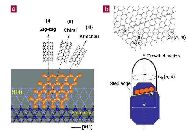
36 Experimental Clues Co catalyst H. Zhu et al., J. Cryst. Growth. 310, 5473 (2008) The nanotube chirality could be associated with the angle of the step edge on (111) plane of the catalyst with respect to the growth direction of CNT 36
37
 Structural correlation between the unrolled honeycomb")


38 (a) (-2 1 1) (b) Step edge (0 1-1) (1 1 1) C h Step edge Carbon atom Iron surface atom (a) Structural correlation between the unrolled honeycomb lattice of a nanotube and the underlying FCC Fe (1 1 1) surface, and (b) schematic diagram illustrates how nanotube chirality forms at the step edge. C h represents the nanotube chiral vector as determined by the step edge, which is directly related to the chiral angle and tube diameter d (d=c h /2).
 D/D, / Fe (1 1 0) (Diameter, Chiral angle) D/D, / (15, 0) (1.182nm, 0) (1.173, 0) D/D=-0.761%, /=0% (1.198, 0) D/D=1.354%, /=0% (1.173, 0) D/D=-0.761%, /=0% (14, 2) (1.")
 D/D=-12.036%, /=- 6.044% (1.229, 12.995) D/D=1.319%, /=-0.069% (1.205, 13.263) D/D=-0.660%, /=1.992% (12, 6) (1.251nm, 19.107) (1.257, 21.054) D/D=0.480%, /=10.190% (1.")
 D/D=-0.384%, /=1.811% (10, 10) (1.365nm, 30) (1.354, 30.003) D/D=-0.806%, /=0.01% (1.407, 31.608) D/D=3.077%, /=5.360% (1.418, 29.173) D/D=3.883%, /=-2.")
39 (n, m) (Diameter, Chiral angle) The Best matches for each SWCNT structures with Low-indexes facets of Fe catalyst at 860C Fe (1 1 1) (Diameter, Chiral angle) D/D, / Fe (1 0 0) (Diameter, Chiral angle) D/D, / Fe (1 1 0) (Diameter, Chiral angle) D/D, / (15, 0) (1.182nm, 0) (1.173, 0) D/D=-0.761%, /=0% (1.198, 0) D/D=1.354%, /=0% (1.173, 0) D/D=-0.761%, /=0% (14, 2) (1.190nm, 6.587) (1.113, 5.818) D/D=-6.471%, /= % (1.394, 7.595) D/D=17.143%, /=15.303% (1.246, 6.371) D/D=4.706%, /=-3.279% (13, 4) (1.213nm, ) (1.067, ) D/D= %, /= % (1.229, ) D/D=1.319%, /=-0.069% (1.205, ) D/D=-0.660%, /=1.992% (12, 6) (1.251nm, ) (1.257, ) D/D=0.480%, /=10.190% (1.370, ) D/D=9.512%, /=2.863% (1.306, ) D/D=4.396%, /=-3.077% (11, 8) (1.302nm, ) (1.361, ) D/D=4.531%, /=-1.146% (1.319, ) D/D=1.306%, /=-0.065% (1.297, ) D/D=-0.384%, /=1.811% (10, 10) (1.365nm, 30) (1.354, ) D/D=-0.806%, /=0.01% (1.407, ) D/D=3.077%, /=5.360% (1.418, ) D/D=3.883%, /=-2.757%
40 Summary There is definite correlation between catalyst facet structures and grown SWCNT chiralities So, problem of selective growth of SWCNTs became a problem of our capability to make nanocatalysts with preferable facets How to solve this problem at elevated temperatures? Confidential 2009 Honda Research Institute USA, 40 Inc.
41 Preferential growth of specific facets by using proper adgas along with hydrocarbon source (e.g. CO/CH 4, CO 2 /CH 4, H 2 O/CH 4, CH 4 /C 2 H 4, ) (100) 111 = 1.97 J/ m = 2.2 J/ m = 2.1 J/ m 2 (111) (110) 111 = 1.5 J/ m = 2.2 J/ m = 2.1 J/ m = 1.97 J/ m = 1.5 J/ m = 2.1 J/ m 2 Confidential 111 = 1.97 J/ m = 2.2 J/ m = 1.7 J/ m Honda Research Institute USA, Inc.
42 Substrate effect FCC particle with (100) facet up (100) 111 = 1.97 J/ m = 2.2 J/ m = 2.1 J / m 2 (no interaction) (110) (111) A weak interaction Some interaction Strong interaction IC-2/55 lecture Confidential 2009 Honda Research Institute USA, 42 Inc.
 Light drawings correspond Confidential 2009 Honda Research Institute USA, 43 Inc.")
43 Pd particle on MgO annealed in UHV (T=550 o C) Pd particle on MgO annealed in O 2 (10-3 Torr at 550 o C) Light drawings correspond Confidential 2009 Honda Research Institute USA, 43 Inc.
Supporting Online Material for
 www.sciencemag.org/cgi/content/full/326/5949/116/dc1 Supporting Online Material for Preferential Growth of Single-Walled Carbon Nanotubes with Metallic Conductivity Avetik R. Harutyunyan,* Gugang Chen,
Carbon Nanotubes by Microwave Plasma-Enhanced Chemical Vapor Deposition
 Carbon Nanotubes by Microwave Plasma-Enhanced Chemical Vapor Deposition M. Maschmann 2, A. Goyal 3, Z. Iqbal 3, T.S. Fisher 2, R. Gat 1 1. Seki Technotron USA. Santa Clara CA, USA. rgat@sekitech.com 2.
Continuous Synthesis of Carbon Nanoclusters Using Well-Controlled Thermal Plasmas
 Continuous Synthesis of Carbon Nanoclusters Using Well-Controlled Thermal Plasmas T. Ohishi*, Y. Yoshihara and O. Fukumasa Graduate School of Science and Engineering, Yamaguchi University, 2-16-1 Tokiwadai,
Floating Catalyst CVD Method. Single- and Double-walled Carbon Nanotubes. Hui-Ming Cheng
 Floating Catalyst CVD Method for Controllable Synthesis of Single- and Double-walled Carbon Nanotubes Hui-Ming Cheng Shenyang National Laboratory for Materials Science Institute of Metal Research, Chinese
Visit
 Practical Applications for Nano- Electronics by Vimal Gopee E-mail: Vimal.gopee@npl.co.uk 10/10/12 Your Delegate Webinar Control Panel Open and close your panel Full screen view Raise hand for Q&A at the
Collopuim CNT 班 M2 竹下弘毅
 Collopuim CNT 班 M2 竹下弘毅 Reference [1]Chin Li Cheung, Andrea Kurtz, Hongkun Park,*, and Charles M. Lieber*, J. Phys. Chem. B 2002, 106, 2429-2433 [2] Daisuke Takagi, Yoshikazu Homma, Hiroki Hibino,Satoru
Supporting Information
 Copyright WILEY VCH Verlag GmbH & Co. KGaA, 69469 Weinheim, Germany, 2012. Supporting Information for Small, DOI: 10.1002/smll. 201102654 Large-Area Vapor-Phase Growth and Characterization of MoS 2 Atomic
Complementary in-situ probes for. Graphene and CNT CVD. Department of Engineering
 Complementary in-situ probes for Graphene and CNT CVD Department of Engineering In-situ nanometrology mean free path of e - scattering in gas: λ e = 1/nσ = kt/pσ for electron energy of 20keV, and p=1mbar
Effects of Hydrogen Flow Rate on Carbon Nanotube Growth
 Effects of Hydrogen Flow Rate on Carbon Nanotube Growth Carolyn Reynolds*, Binh Duong**, and Supapan Seraphin** *Dept. Optical Engineering, Norfolk State University, Norfolk, VA 23504; **Dept. Materials
Inherent Predominance of High Chiral Angle Metallic Carbon Nanotubes in Continuous Fibers Grown From Molten Catalyst
 Electronic Supplementary Material (ESI) for Nanoscale. This journal is The Royal Society of Chemistry 2016 Inherent Predominance of High Chiral Angle Metallic Carbon Nanotubes in Continuous Fibers Grown
The effects of Fe/Al 2 O 3 preparation technique as a catalyst on synthesized CNTs in CVD method.
 Science Journal of Physics Science Journal Publication Science Journal of Physics Web: http://www.sjpublication.com/sjp.html The effects of Fe/Al 2 O 3 preparation technique as a catalyst on synthesized
Oxidative corrosion potential vs. ph diagram for single-walled carbon
 Electronic Supplementary Material (ESI) for RSC Advances. This journal is The Royal Society of Chemistry 2014 Electronic Supplementary Information (ESI) Oxidative corrosion potential vs. ph diagram for
Nano Fabrication Research at FIU
 Nano Fabrication Research at FIU Professor W. Choi s Nano Materials and Devices Lab FIU logo with 25nm line width by e-beam lithography Fastest growing University in the US- Ranked in top 25 largest Universities
Tough Materials: Shear Bands & Crazes
 Tough Materials: Shear Bands & Crazes Polycarbonate Images removed due to copyright restrictions. Please see, for example, http://www.doitpoms.ac.uk/miclib/micrograph.php?id=559 http://www.doitpoms.ac.uk/miclib/micrograph.php?id=592
SUPPLEMENTARY INFORMATION
 Supplementary Figures SUPPLEMENTARY INFORMATION Supplementary Figure S1. Schematic Representation of temperature-controlled sonication apparatus. 1 Solution Abs (a.u.) 0.18 HiPco SWNT Dispersion in rr-p3ddt/toluene
Defense Technical Information Center Compilation Part Notice
 UNCLASSIFIED Defense Technical Information Center Compilation Part Notice ADP012180 TITLE: Growth of Highly Oriented ZnO Nanorods by Chemical Vapor Deposition DISTRIBUTION: Approved for public release,
Enhancement of connectivity and flux pinning in MgB2 superconducting bulks and wires
 University of Wollongong Research Online University of Wollongong Thesis Collection 1954-2016 University of Wollongong Thesis Collections 2009 Enhancement of connectivity and flux pinning in MgB2 superconducting
Aligned Carbon Nanofibre-Polymer Composite Membranes. CNT Growth and Manipulation. Eleanor Campbell Dept. of Physics, Göteborg University
 Aligned Carbon Nanofibre-Polymer Composite Membranes CNT Growth and Manipulation Eleanor Campbell Dept. of Physics, Göteborg University Plasma CVD Growth Polymer/Nanofibre Composite Low ambient temperature
Supplementary Figure 1. Schematic for the growth of high-quality uniform
 Supplementary Figure 1. Schematic for the growth of high-quality uniform monolayer WS 2 by ambient-pressure CVD. Supplementary Figure 2. Schematic structures of the initial state (IS) and the final state
the image contrast at the atomic scale. The same method for STM image
 1 2 3 4 5 6 7 8 9 10 11 12 13 14 15 16 17 18 19 20 21 22 23 24 25 26 27 28 29 Supplementary Note 1. The interpretation of element-specific scanning tunneling microscopy (STM) images Oxygen vacancy lines
Boron Nitride. can you spot the adamantane-like rings? After that little tangent on graphitic carbon nitride -back to diamondoids
 After that little tangent on graphitic carbon nitride -back to diamondoids Boron Nitride isoelectronic with carbon exists as various polymorphs, one is analogous to diamond and one to graphite. diamond-like
SiC crystal growth from vapor
 SiC crystal growth from vapor Because SiC dissolves in Si and other metals can be grown from melt-solutions: Liquid phase epitaxy (LPE) Solubility of C in liquid Si is 0.029% at 1700oC high T process;
Nucleation and growth of nanostructures and films. Seongshik (Sean) Oh
 Oh") Nucleation and growth of nanostructures and films Seongshik (Sean) Oh Outline Introduction and Overview 1. Thermodynamics and Kinetics of thin film growth 2. Defects in films 3. Amorphous, Polycrystalline
Nucleation and growth of nanostructures and films Seongshik (Sean) Oh Outline Introduction and Overview 1. Thermodynamics and Kinetics of thin film growth 2. Defects in films 3. Amorphous, Polycrystalline
ZnO thin film deposition on sapphire substrates by chemical vapor deposition
 ZnO thin film deposition on sapphire substrates by chemical vapor deposition Zhuo Chen 1, T. Salagaj 2, C. Jensen 2, K. Strobl 2, Mim Nakarmi 1, and Kai Shum 1, a 1 Physics Department, Brooklyn College
CEMS study on diluted magneto titanium oxide films prepared by pulsed laser deposition
 Hyperfine Interact (2006) 168:1065 1071 DOI 10.1007/s10751-006-9406-2 CEMS study on diluted magneto titanium oxide films prepared by pulsed laser deposition K. Nomura & K. Inaba & S. Iio & T. Hitosugi
Ag 2 S: Fabrication and Characterization Techniques
 2 2 S: Fabrication and Characterization Techniques This chapter describes two fabrication methods used for the growth of 2 S thin films. The specific growth parameters are presented for each method as
Preparation and characterization of Co BaTiO 3 nano-composite films by the pulsed laser deposition
 Journal of Crystal Growth 289 (26) 48 413 www.elsevier.com/locate/jcrysgro Preparation and characterization of Co BaTiO 3 nano-composite films by the pulsed laser deposition Wu Weidong a,b,, He Yingjie
CHAPTER 5 EFFECT OF POST DEPOSITION ANNEALING ON THE SURFACE MORPHOLOGY OF THE DLC FILM
 86 CHAPTER 5 EFFECT OF POST DEPOSITION ANNEALING ON THE SURFACE MORPHOLOGY OF THE DLC FILM 5.1 INTRODUCTION Among various amorphous carbon films, DLC films produced via RF-PECVD have been successfully
Yilong Han, Co-authors: Yi Peng, Feng Wang Nucleation in solid-solid transitions of colloidal crystals
 Yilong Han, yilong@ust.hk Co-authors: Yi Peng, Feng Wang Nucleation in solid-solid transitions of colloidal crystals Solid-solid phase transitions between different crystalline structures are ubiquitous
Oxidation behavior of Cu nanoclusters in hybrid thin films
 Oxidation behavior of Cu nanoclusters in hybrid thin films Harm Wulff,* Steffen Drache*, Vitezslav Stranak**, Angela Kruth*** *EMAU Greifswald, **South Bohemian University, Budweis, *** INP Greifswald
Heteroepitaxy of Monolayer MoS 2 and WS 2
 Supporting Information Seed Crystal Homogeneity Controls Lateral and Vertical Heteroepitaxy of Monolayer MoS 2 and WS 2 Youngdong Yoo, Zachary P. Degregorio, James E. Johns* Department of Chemistry, University
FePd (216 Å) grown on (001) MgO. 2θ(deg)
 grown on (001) MgO. 2θ(deg)") Major Findings 1. FePd thin films The structural characterization of the films grown at various substrate temperatures (RT- 700 o C) was performed ex-situ using X-Ray Diffraction (XRD). The optimum substrate
Major Findings 1. FePd thin films The structural characterization of the films grown at various substrate temperatures (RT- 700 o C) was performed ex-situ using X-Ray Diffraction (XRD). The optimum substrate
From sand to silicon wafer
 From sand to silicon wafer 25% of Earth surface is silicon Metallurgical grade silicon (MGS) Electronic grade silicon (EGS) Polycrystalline silicon (polysilicon) Single crystal Czochralski drawing Single
hydrogen evolution reaction
 Conducting MoS 2 nanosheets as catalysts for hydrogen evolution reaction Damien Voiry, Maryam Salehi, Rafael Silva +, Takeshi Fujita #, Mingwei Chen #, Tewodros Asefa +, Vivek Shenoy, Goki Eda $,$$, and
Synthesis of nanocarbon materials by PECVD: challenges to direct synthesis via CO 2 reduction using plasma-soec hybrid reactor
 22 nd International Symposium on Plasma Chemistry July 5-10, 2015; Antwerp, Belgium Synthesis of nanocarbon materials by PECVD: challenges to direct synthesis via CO 2 reduction using plasma-soec hybrid
SRI LANKAN GRAPHITE MAKING THE SPACE ELEVATOR POSSIBLE
 SRI LANKAN GRAPHITE MAKING THE SPACE ELEVATOR POSSIBLE Samaranayake, B. G. L. T. 1,Gunasekera, S. 2,Kumarasinghe, A. K. R. 1, and Kottegoda, N. S. 1 1 Senior Scientist, 2 Technical Services Manager, NANCO
Supplementary Information
 Supplementary Information Atmospheric microplasma-functionalized 3D microfluidic strips within dense carbon nanotube arrays confine Au nanodots for SERS sensing Samuel Yick, Zhao Jun Han and Kostya (Ken)
SUPPLEMENTARY INFORMATION
 High Electrochemical Activity of the Oxide Phase in Model Ceria- and Ceria-Ni Composite Anodes William C. Chueh 1,, Yong Hao, WooChul Jung, Sossina M. Haile Materials Science, California Institute of Technology,
Dual Catalytic Purpose of the Tungsten Filament During the. Synthesis of Single-Helix Carbon Microcoils by Hot-Wire CVD
 Dual Catalytic Purpose of the Tungsten Filament During the Synthesis of Single-Helix Carbon Microcoils by Hot-Wire CVD C. J. Oliphant 1,2, C. J. Arendse 1,, G. F. Malgas 1, D. E. Motaung 1,2, T. F. G.
Lateral epitaxial growth of two-dimensional layered semiconductor heterojunctions
 Lateral epitaxial growth of two-dimensional layered semiconductor heterojunctions Xidong Duan, Chen Wang, Jonathan Shaw, Rui Cheng, Yu Chen, Honglai Li, Xueping Wu, Ying Tang, Qinling Zhang, Anlian Pan,
Supplementary Information
 Supplementary Information Direct manufacturing of ultrathin graphite on three- dimensional nanoscale features Mercè Pacios, Peiman Hosseini, Ye Fan, Zhengyu He, Oliver Krause, John Hutchison, Jamie H.
Supplementary Information
 Supplementary Information Supplementary Figure 1 Characterization of precursor coated on salt template. (a) SEM image of Mo precursor coated on NaCl. Scale bar, 50 μm. (b) EDS of Mo precursor coated on
6.8 Magnetic in-plane anisotropy of epitaxially grown Fe-films on vicinal Ag(001) and Au(001) with different miscut orientations
 and Au(001) with different miscut orientations") C. Epitaxial Growth 6.8 Magnetic in-plane anisotropy of epitaxially grown Fe-films on vicinal Ag(001) and Au(001) with different miscut orientations M. Rickart, A.R. Frank, J. Jorzick, Ch. Krämer, S.O.
C. Epitaxial Growth 6.8 Magnetic in-plane anisotropy of epitaxially grown Fe-films on vicinal Ag(001) and Au(001) with different miscut orientations M. Rickart, A.R. Frank, J. Jorzick, Ch. Krämer, S.O.
Thin Film by Chemical Vapor Deposition
 Supporting Materials Synthesis of Few-Layer Hexagonal Boron Nitride Thin Film by Chemical Vapor Deposition Yumeng Shi,, Christoph Hamsen,, Xiaoting Jia, Ki Kang Kim, Alfonso Reina, Mario Hofmann, Allen
Journal of Chemical and Pharmaceutical Research, 2017, 9(1): Research Article
: Research Article") Available online www.jocpr.com Journal of Chemical and Pharmaceutical Research, 2017, 9(1):163-167 Research Article ISSN : 0975-7384 CODEN(USA) : JCPRC5 Synthesis and Characterization of Carbon Nano Spheres
Available online www.jocpr.com Journal of Chemical and Pharmaceutical Research, 2017, 9(1):163-167 Research Article ISSN : 0975-7384 CODEN(USA) : JCPRC5 Synthesis and Characterization of Carbon Nano Spheres
SUPPLEMENTARY INFORMATION
 doi:10.1038/nature11562 Figure S1 Distinction of graphene and copper grain boundaries. a-b, SEM images of oxidised graphene/cu at different magnifications. The white dotted lines indicate the oxidised
Crystal morphology and growth in annealed rubrene thin films
 Supporting Information Crystal morphology and growth in annealed rubrene thin films Thomas R. Fielitz and Russell J. Holmes In the majority of this paper, the polymorph composition is inferred from the
Supporting Information
 Supporting Information Large-Area, Transfer-Free, Oxide-Assisted Synthesis of Hexagonal Boron Nitride Films and Their Heterostructures with MoS2 and WS2 Sanjay Behura, Phong Nguyen, Songwei Che, Rousan
ALD of Copper and Copper Oxide Thin Films for Applications in Metallization Systems of ULSI Devices
 ALD of Copper and Copper Oxide Thin Films for Applications in Metallization Systems of ULSI Devices a, Steffen Oswald b, Nina Roth c, Heinrich Lang c, Stefan E. Schulz a,d, and Thomas Gessner a,d a Center
Outline. L13. Mechanics of Nanostructures: Tensile Loading and Fracture Mechanics
 L13. Mechanics of Nanostructures: Tensile Loading and Fracture Mechanics Outline 1. Introduction 2. Tensile Test work overview 3. Recent work in Ruoff group Carbon nanocoil Crystalline Boron Nanowire Arc-grown
Pre-treatment of low temperature GaN buffer layer deposited on AlN Si substrate by hydride vapor phase epitaxy
 Ž. Surface and Coatings Technology 131 000 465 469 Pre-treatment of low temperature GaN buffer layer deposited on AlN Si substrate by hydride vapor phase epitaxy Ha Jin Kim, Ho-Sun Paek, Ji-Beom Yoo Department
Steric Effects on the. Transition in YH x
 Steric Effects on the Metallic-Mirror Mirror to Transparent-Insulator Transition in YH x Troy C. Messina Department of Physics University of Texas at Austin Final Defense 22 November 2002 Outline Introduction
Supplementary Figure 1. Crystal structures of conventional layered and Li-rich layered manganese oxides. a, The crystal structure of rhombohedral
 Supplementary Figure 1. Crystal structures of conventional layered and Li-rich layered manganese oxides. a, The crystal structure of rhombohedral LiMO 2 (M = Ni, Co, Mn) with the space group R3m. b, The
Chapter 9 Phase Diagrams. Dr. Feras Fraige
 Chapter 9 Phase Diagrams Dr. Feras Fraige Chapter Outline Definitions and basic concepts Phases and microstructure Binary isomorphous systems (complete solid solubility) Binary eutectic systems (limited
arxiv:cond-mat/ v2 [cond-mat.mtrl-sci] 29 Nov 2003
![arxiv:cond-mat/ v2 [cond-mat.mtrl-sci] 29 Nov 2003](/thumbs/93/114120274.jpg "arxiv:cond-mat/ v2 [cond-mat.mtrl-sci] 29 Nov 2003") Fabrication and Electrical Properties of Pure Phase Films B. G. Chae, D. H. Youn, H. T. Kim, S. Maeng, and K. Y. Kang Basic Research Laboratory, ETRI, Daejeon 305-350, Republic of Korea arxiv:cond-mat/0311616v2
Fabrication and Electrical Properties of Pure Phase Films B. G. Chae, D. H. Youn, H. T. Kim, S. Maeng, and K. Y. Kang Basic Research Laboratory, ETRI, Daejeon 305-350, Republic of Korea arxiv:cond-mat/0311616v2
Module 29. Precipitation from solid solution I. Lecture 29. Precipitation from solid solution I
 Module 29 Precipitation from solid solution I Lecture 29 Precipitation from solid solution I 1 Keywords : Properties of two phase alloys, super saturated solid solutions, historical perspective, solution
MICROSTRUCTURE AND PROPERTIES OD RAPID SOLIDIFIED AL-SI-FE AND AL-SI-FE-CR ALLOYS PREPARED BY CENTRIFUGAL ATOMIZATION. Filip PRŮŠA*, Dalibor VOJTĚCH
 MICROSTRUCTURE AND PROPERTIES OD RAPID SOLIDIFIED AL-SI-FE AND AL-SI-FE-CR ALLOYS PREPARED BY CENTRIFUGAL ATOMIZATION Filip PRŮŠA*, Dalibor VOJTĚCH Department of Metals and Corrosion Engineering, Institute
but T m (Sn0.62Pb0.38) = 183 C, so this is a common soldering alloy.
 = 183 C, so this is a common soldering alloy.") T m (Sn) = 232 C, T m (Pb) = 327 C but T m (Sn0.62Pb0.38) = 183 C, so this is a common soldering alloy. T m (Au) = 1064 C, T m (Si) = 2550 C but T m (Au0.97Si0.03) = 363 C, so thin layer of gold is used
T m (Sn) = 232 C, T m (Pb) = 327 C but T m (Sn0.62Pb0.38) = 183 C, so this is a common soldering alloy. T m (Au) = 1064 C, T m (Si) = 2550 C but T m (Au0.97Si0.03) = 363 C, so thin layer of gold is used
Controllable Growth of Semiconductor Heterostructures Mediated by Bifunctional Ag 2 S Nanocrystals as Catalyst or Source-Host
 Controllable Growth of Semiconductor Heterostructures Mediated by Bifunctional Ag 2 S Nanocrystals as Catalyst or Source-Host Guoxing Zhu and Zheng Xu Nanjing National Laboratory of Solid State Microstructure,
Low temperature carbon material deposition with photo-enhanced chemical vapor deposition
 Louisiana State University LSU Digital Commons LSU Doctoral Dissertations Graduate School 2012 Low temperature carbon material deposition with photo-enhanced chemical vapor deposition KyungNam Kang Louisiana
Blueshift of optical band gap in ZnO thin films grown by metal-organic chemical-vapor deposition
 JOURNAL OF APPLIED PHYSICS 98, 013505 2005 Blueshift of optical band gap in ZnO thin films grown by metal-organic chemical-vapor deposition S. T. Tan, B. J. Chen, X. W. Sun, a and W. J. Fan School of Electrical
Chapter 10, Phase Transformations
 Chapter Outline: Phase Transformations Heat Treatment (time and temperature) Microstructure Kinetics of phase transformations Homogeneous and heterogeneous nucleation Growth, rate of the phase transformation
Carbon nanotubes formation by short-time ball milling and annealing of graphite
 OPTOELECTRONİCS AND ADVANCED MATERİALS RAPID COMMUNICATIONS Vol. 6, No. 1-2, January-February 2012, p. 183-187 Carbon nanotubes formation by short-time ball milling and annealing of graphite ÖMER GÜLER
The Global Market for Single-Walled Carbon Nanotubes TABLE OF CONTENTS 1 RESEARCH METHODOLOGY... 18
 TABLE OF CONTENTS 1 RESEARCH METHODOLOGY... 18 1.1 Market opportunity rating system... 18 1.2 Market challenges rating system... 20 2 EXECUTIVE SUMMARY... 23 2.1 Exceptional properties... 24 2.2 Products
More Thin Film X-ray Scattering and X-ray Reflectivity
 Stanford Synchrotron Radiation Laboratory More Thin Film X-ray Scattering and X-ray Reflectivity Mike Toney, SSRL 1. Introduction (real space reciprocal space) 2. Polycrystalline film (no texture) RuPt
A scalable CVD synthesis of high-purity single-walled carbon nanotubes with porous MgO as support material
 A scalable CVD synthesis of high-purity single-walled carbon nanotubes with porous MgO as support material Li Qingwen, Yan Hao, Cheng Yan, Zhang Jin* and Liu Zhongfan* Centre for Nanoscale Science and
Supplementary Information
 Supplementary Information Growth kinetics of white graphene (h-bn) on a planarised Ni foil surface Hyunjin Cho 1,4, Sungchan Park 1, Dong-Il Won 2, Sang Ook Kang 2, Seong-Soo Pyo 3, Dong-Ik Kim 3, Soo
SYNTHESIS OF CARBON NANOPARTICLES BY ARC DISCHARGE IN LIQUID NITROGEN USING METAL-GRAPHITE ELECTRODES
 SYNTHESIS OF CARBON NANOPARTICLES BY ARC DISCHARGE IN LIQUID NITROGEN USING METAL-GRAPHITE ELECTRODES T. Charinpanitkul* and E. Phattarapongsant, Center of Excellence in Particle Technology (CEPT), Faculty
Synthesis and Laser Processing of ZnO Nanocrystalline Thin Films. GPEC, UMR 6631 CNRS, Marseille, France.
 TH.B 9.45 O Synthesis and Laser Processing of ZnO Nanocrystalline Thin Films I. Ozerov 1, D. Nelson 2, A.V. Bulgakov 3, W. Marine* 1, and M. Sentis 4 1 GPEC, UMR 6631 CNRS, 13288 Marseille, France. 2 A.F.
How can we describe a crystal?
 How can we describe a crystal? Examples of common structures: (1) The Sodium Chloride (NaCl) Structure (LiH, MgO, MnO, AgBr, PbS, KCl, KBr) The NaCl structure is FCC The basis consists of one Na atom and
Materials Characterization
 Materials Characterization C. R. Abernathy, B. Gila, K. Jones Cathodoluminescence (CL) system FEI Nova NanoSEM (FEG source) with: EDAX Apollo silicon drift detector (TE cooled) Gatan MonoCL3+ FEI SEM arrived
Synthesis of aligned carbon nanotubes on double-sided metallic substrate by chemical vapor deposition
 Synthesis of aligned carbon nanotubes on double-sided metallic substrate by chemical vapor deposition Huan Wang, Jiyun Feng, Xijun Hu and Ka Ming Ng* Department of Chemical Engineering Hong Kong University
Epitaxial growth of (001) and (111) Ni films on MgO substrates
 and (111) Ni films on MgO substrates") Epitaxial growth of (001) and (111) Ni films on MgO substrates Rosa Alejandra Lukaszew 1, Vladimir Stoica, Ctirad Uher and Roy Clarke Physics Department, University of Michigan, Ann Arbor 1 Presently at
Epitaxial growth of (001) and (111) Ni films on MgO substrates Rosa Alejandra Lukaszew 1, Vladimir Stoica, Ctirad Uher and Roy Clarke Physics Department, University of Michigan, Ann Arbor 1 Presently at
1. Use the Ellingham Diagram (reproduced here as Figure 0.1) to answer the following.
 to answer the following.") 315 Problems 1. Use the Ellingham Diagram (reproduced here as Figure 0.1) to answer the following. (a) Find the temperature and partial pressure of O 2 where Ni(s), Ni(l), and NiO(s) are in equilibrium.
315 Problems 1. Use the Ellingham Diagram (reproduced here as Figure 0.1) to answer the following. (a) Find the temperature and partial pressure of O 2 where Ni(s), Ni(l), and NiO(s) are in equilibrium.
Defense Technical Information Center Compilation Part Notice
 UNCLASSIFIED Defense Technical Information Center Compilation Part Notice ADP012154 TITLE: Structural Characterization of GaN Nanowires Fabricated via Direct Reaction of Ga Vapor and Ammonia DISTRIBUTION:
Structure and Chemical Analysis of Carbon Nanotubes Grown on Diamond Substrate Using Three Different Techniques MRS: November 30, 2010
 Structure and Chemical Analysis of Carbon Nanotubes Grown on Diamond Substrate Using Three Different Techniques MRS: November 30, 2010 Betty T. Quinton Wright State University, PhD. Student Material Science
Effect of titanium additions to low carbon, low manganese steels on sulphide precipitation
 University of Wollongong Thesis Collections University of Wollongong Thesis Collection University of Wollongong Year 2008 Effect of titanium additions to low carbon, low manganese steels on sulphide precipitation
Equilibria in Materials
 2009 fall Advanced Physical Metallurgy Phase Equilibria in Materials 09.01.2009 Eun Soo Park Office: 33-316 Telephone: 880-7221 Email: espark@snu.ac.kr Office hours: by an appointment 1 Text: A. PRINCE,
CHAPTER 4 THE STUDIES OF THE CVD GROWTH PROCESS FOR EPITAXIAL DIAMOND (100) FILMS USING UHV STM
 FILMS USING UHV STM") CHAPTER 4 THE STUDIES OF THE CVD GROWTH PROCESS FOR EPITAXIAL DIAMOND (100) FILMS USING UHV STM 4.1 Introduction This chapter presents studies of the CVD diamond growth process using UHV STM. It has been
CHAPTER 4 THE STUDIES OF THE CVD GROWTH PROCESS FOR EPITAXIAL DIAMOND (100) FILMS USING UHV STM 4.1 Introduction This chapter presents studies of the CVD diamond growth process using UHV STM. It has been
Synthesis and Evaluation of Electrocatalysts for Fuel Cells
 Synthesis and Evaluation of Electrocatalysts for Fuel Cells Jingguang Chen Center for Catalytic Science and Technology (CCST) Department of Chemical Engineering University of Delaware Newark, DE 19711
Multibranching Carbon Nanotubes via Self-Seeded Catalysts
 Multibranching Carbon Nanotubes via Self-Seeded Catalysts NANO LETTERS 2006 Vol. 6, No. 2 324-328 Joseph F. AuBuchon, Li-Han Chen, Chiara Daraio, and Sungho Jin* Materials Science and Engineering Program,
Scale-Up of Carbon Nanotube Synthesis at the Jefferson Lab Free Electron Laser: From Research to Production
 Scale-Up of Carbon Nanotube Synthesis at the Jefferson Lab Free Electron Laser: From Research to Production Michael W. Smith 1, Kevin Jordan 2, Cheol Park 3, Michelle Shinn 2, Brian Holloway 4, 1 NASA
Time-resolved diffraction profiles and structural dynamics of Ni film under short laser pulse irradiation
 IOP Publishing Journal of Physics: Conference Series 59 (2007) 11 15 doi:10.1088/1742-6596/59/1/003 Eighth International Conference on Laser Ablation Time-resolved diffraction profiles and structural dynamics
Effect of normalization on the microstructure and texture evolution during primary and secondary recrystallization of Hi-B electrical steel
 Indian Journal of Engineering & Materials Sciences Vol. 23, April & June 2016, pp. 165-170 Effect of normalization on the microstructure and texture evolution during primary and secondary recrystallization
Growth of bulk single crystals β-fesi 2 by chemical vapour deposition
 Vol. 46 No. 1 SCIENCE IN CHINA (Series G) February 2003 Growth of bulk single crystals β-fesi 2 by chemical vapour deposition LI Yanchun ( ) 1,2, SUN Liling ( ) 1,3,CAOLimin( ) 1, ZHAO Jianhua ( ) 2,WANGHaiyan(
Growth of large single-crystalline two-dimensional boron. nitride hexagons on electropolished copper
 Supporting Information Growth of large single-crystalline two-dimensional boron nitride hexagons on electropolished copper Roland Yingjie Tay,, Mark H. Griep, Govind Mallick,, Siu Hon Tsang, Ram Sevak
Phase Diagrams of Pure Substances Predicts the stable phase as a function of P total and T. Example: water can exist in solid, liquid and vapor
 PHASE DIAGRAMS Phase a chemically and structurally homogenous region of a material. Region of uniform physical and chemical characteristics. Phase boundaries separate two distinct phases. A single phase
Controllable Growth of Few-layer Spiral WS 2
 Electronic Supplementary Material (ESI) for RSC Advances. This journal is The Royal Society of Chemistry 2015 Supporting Information Controllable Growth of Few-layer Spiral WS 2 Prasad V. Sarma, Prasanna
Lecture contents. Heteroepitaxy Growth technologies Strain Misfit dislocations. NNSE 618 Lecture #24
 1 Lecture contents Heteroepitaxy Growth technologies Strain Misfit dislocations Epitaxy Heteroepitaxy 2 Single crystalline layer on Single crystalline substrate Strong layer-substrate interaction orientation
Carbon nanotubes are impressive because
 Revealing the Impact of Catalyst Phase Transition on Carbon Nanotube Growth by in Situ Raman Spectroscopy Rahul Rao,,,r, * Neal Pierce,, David Liptak,,^ Daylond Hooper,,^ Gordon Sargent,,^ S. Lee Semiatin,
Dual-function Metal-Organic Frameworks Based Wearable Fibers for Gas Probing and Energy Storage
 Supporting Information Dual-function Metal-Organic Frameworks Based Wearable Fibers for Gas Probing and Energy Storage Kun Rui, Xiaoshan Wang, Min Du, Yao Zhang, Qingqing Wang, Zhongyuan Ma, Qiao Zhang,
In Situ XRD and TEM Studies of Sol-Gel-based. Synthesis of LiFePO4
 In Situ XRD and TEM Studies of Sol-Gel-based Synthesis of LiFePO4 Dominika A. Ziolkowska a,*, Jacek B. Jasinski b,*, Bartosz Hamankiewicz c, Krzysztof P. Korona a, She-Huang Wu d and Andrzej Czerwinski
Thermochromic halide perovskite solar cells
 SUPPLEMENTARY INFORMATION Articles https://doi.org/10.1038/s41563-017-0006-0 In the format provided by the authors and unedited. Thermochromic halide perovskite solar cells Jia Lin 1,2,3, Minliang Lai
Metal-containing diamond-like carbon with self-assembled alternating nano-scaled layers
 Metal-containing diamond-like carbon with self-assembled alternating nano-scaled layers Wan-Yu Wu, Jyh-Ming Ting* Mina Materials Laboratory, Department of Materials Science and Engineering, National Cheng
Electron Microscopy Investigation at the Initial Growth Stage of Carbon Nanotubes
 Journal of the Korean Physical Society, Vol. 42, February 2003, pp. S727 S731 Electron Microscopy Investigation at the Initial Growth Stage of Carbon Nanotubes Sung-Jin Eum, Hee-Kwang Kang, Cheol-Woong
Combinatorial RF Magnetron Sputtering for Rapid Materials Discovery: Methodology and Applications
 Combinatorial RF Magnetron Sputtering for Rapid Materials Discovery: Methodology and Applications Philip D. Rack,, Jason D. Fowlkes, and Yuepeng Deng Department of Materials Science and Engineering University
3C-SiC growth on Si substrates via CVD: An introduction
 3C-SiC growth on Si substrates via CVD: An introduction Written by Jessica Eid LMGP/INPG, France, jessica.eid@inpg.fr and Irina Georgiana Galben LMGP/INPG, France, irina.galben@inpg.fr based on the lecture
SUPPLEMENTARY INFORMATION
 Grains and grain boundaries in highly crystalline monolayer molybdenum disulphide Supplementary Figure S1: Commonly-observed shapes in MoS 2 CVD. Optical micrographs of various CVD MoS2 crystal shapes
Physics and Material Science of Semiconductor Nanostructures
 Physics and Material Science of Semiconductor Nanostructures PHYS 570P Prof. Oana Malis Email: omalis@purdue.edu Lecture 6 Bulk semiconductor growth Single crystal techniques Nanostructure fabrication
Supporting Online Material for
 www.sciencemag.org/cgi/content/full/science.1200448/dc1 Supporting Online Material for Increasing Solar Absorption for Photocatalysis with Black Hydrogenated Titanium Dioxide Nanocrystals This PDF file