Carbon Nanotubes by Microwave Plasma-Enhanced Chemical Vapor Deposition
|
|
|
- Bruno Floyd
- 5 years ago
- Views:
Transcription
1 Carbon Nanotubes by Microwave Plasma-Enhanced Chemical Vapor Deposition M. Maschmann 2, A. Goyal 3, Z. Iqbal 3, T.S. Fisher 2, R. Gat 1 1. Seki Technotron USA. Santa Clara CA, USA. rgat@sekitech.com 2. Purdue University, School of Mechanical Engineering and Birck Nanotechnology Center 3. New Jersey Institute of Technology, Department of Chemistry


2 MWCNT- 100mm wafer Spin on multiwall catalyst- no sputtering 6nm Fe particles suspended in oil Process: 50% CH4 in H2, 300 W, 5 Torr, 850 C 100 mm
, and")

3 Significance of PECVD Plasma dissociates hydrogen/methane mix into reactive radicals mostly atomic hydrogen (H), and methyl (CH 3 ) Plasma CVD has shown vertically oriented, dense forests of carbon nanotubes. L. C. Chen, National Taiwan Univ

4 600 MWCNT/MWCVD cm(edge) 1 cm 2 cm Raman Shift cm^-1
5 Motivation Provide microwave plasma deposition technology to enable: Large area mm deposition temperature <450C. Particle and impurity control Reliable, reproducible Semiconductor process compatible Reduce required growth temperatures for SWCNTs by thermal CVD from o C. MICROWAVE Plasma generates radical density characteristic of 2000C at much lower effective temperature e.g < 450C and can be highly ionized (Low pressure ECR mode) or highly neutral (high pressure mode).

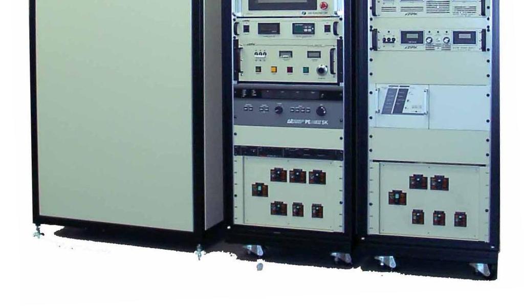
6 Microwave PECVD System Process Gasses: H 2 : sccm CH 4 : 0-10 sccm Substrate DC Bias: V; A 3.5 Kilowatt, 900C RF Heating of 4 Substrate External Interlocks for Safe Hands-Free Operation 1.5kW and 2.5GHz Microwave Generator Vacuum Chamber Dual Wavelength Pyrometer Measures Surface Temperature Embedded K-type thermocouple monitors stage temperature Seki Technotron Corp. AX5200 Series
7 Plasma Deposition system Ellipsometry, IR Pyrometry and laser interferometry Microwave plasma DC bias Substrate RF induction heating water cooled coil thermocouple Pump
8 SWCNT Catalyst Synthesis Catalyst/support made by sol-gel method: Mix powders and form Sol : Magnesium Nitrate Mg(NO 3 ).6H 2 O, 0.5g Cobalt Nitrate Co(NO 3 ).6H 2 O, Ammonium Heptamolybdate (NH 4 ) 6 Mo 7 O 24.4H 2 O, citric acid, 3g distilled water typically 4:1 Mo:Co supported on MgO: MgO (1-x-y) Co x Mo y
9 Catalyst/support Synthesis Solution placed in ceramic boat and loaded into 550 o C furnace for 5 minutes in air Resulting bimetallic Mo:Co catalyst and MgO support was ground to a fine powder using a mortar and pestle grams of powder added to 25mL and ultrasonically agitated for 3 hours before being dispersed onto silicon substrates
10 Synthesis Conditions Current work Catalyst Temperature Pressure Feedstock Gasses Plasma Mo / Co catalyst with C 10 Torr 10:1 H 2 : CH W MgO support Prior PECVD SWCNT but not MICROWAVE plasma: 1) T. Kato et a., Chem. Phys. Lett., 381, 422 (2003). 2) Y. Li et al., Nano Lett., 4, 317 (2004). Catalyst Temperature Pressure Feedstock Gasses Plasma 1 Fe / Co catalyst with Faujasite-type zeolite C 0.5 Torr 7 : 4 H 2 : CH W support Ferratin nanoparticles and 2 sub-monolayer e-beam 600 C 0.5 Torr 1 : 4 Ar : CH 4 75 W evaporated iron

11 SEM Microns long bundles of SWCNTs

12 AFM Image
13 Deposition temperature 800 o C D (disorder)-band at 1308 cm -1 High intensity consistent with a:c or poor resonance condition Intensity (a.u.) G (graphite)-band at 1593 cm Raman shift (cm -1 ) Horiba/Jobin Yvon LabRam system with cooled CCD (charge coupled device) detection and nm laser excitation with 15 mw intensity at the source and approximately 1.5 mw at the sample
14 Deposition temperature 800 o C Radial breathing modes at 189 and 254 cm -1 correspond to 1.3 and 0.9 nm diameter, respectively* Intensity (a.u.) Based on laser excitation energy and Raman shift, 0.9 nm CNTs are semiconducting while 1.3 nm CNTs are metallic** Raman Shift (cm -1 ) *S. M. Bachiloet al., Science, 298, 2361 (2002). **H. Kataura et al., Synth. Met., 103, 2555 (1999).
15 Deposition temperature 600 o C Weak Radial breathing modes at 175, 192, 206, and 226 cm -1 corresponding to diameters from 1.2 to 1.5 nm. Strong D band likely a:c Intensity (a.u.) (b) In te n sity (a.u.) Raman Shift (cm -1 ) Raman Shift (cm -1 )
16 Data: Diamond 2003, 14 th European Conference on Diamond, Diamond-like Materials, Carbon Nanotubes, Nitrides and Silicon Carbide M W and SW CNT deposition temp vs. Pressure (multiple sources) Woo, KIST, Korea, ECR-MW plasma Robertson, Cambridge U., UK, DC plasma Substrate Temp (C) Pressure (Torr)
17 Electron Cyclotron Resonance mtorr Operation Room temperature deposition High rate plasma density radical flux ECR

18 ECR- CNT Deposition System
19 Conclusions Multiwall and Single wall CNT were deposited using Sekitechnotron/ASTeX microwave PECVD. Deposition area 100mm diameter wafers Both semiconducting and metallic SWCNTs were synthesized at 600C and higher temperatures.
20 Acknowledgements NJIT thanks the US Army and NSF Purdue thanks NASA-Purdue Institute for Nanoelectronics and Computing and Birck Nanotechnology Center Sekitechnotron thanks Dr. Tarun Sharda for depositions.
The effects of Fe/Al 2 O 3 preparation technique as a catalyst on synthesized CNTs in CVD method.
 Science Journal of Physics Science Journal Publication Science Journal of Physics Web: http://www.sjpublication.com/sjp.html The effects of Fe/Al 2 O 3 preparation technique as a catalyst on synthesized
Effects of Hydrogen Flow Rate on Carbon Nanotube Growth
 Effects of Hydrogen Flow Rate on Carbon Nanotube Growth Carolyn Reynolds*, Binh Duong**, and Supapan Seraphin** *Dept. Optical Engineering, Norfolk State University, Norfolk, VA 23504; **Dept. Materials
Aligned Carbon Nanofibre-Polymer Composite Membranes. CNT Growth and Manipulation. Eleanor Campbell Dept. of Physics, Göteborg University
 Aligned Carbon Nanofibre-Polymer Composite Membranes CNT Growth and Manipulation Eleanor Campbell Dept. of Physics, Göteborg University Plasma CVD Growth Polymer/Nanofibre Composite Low ambient temperature
Structure and Chemical Analysis of Carbon Nanotubes Grown on Diamond Substrate Using Three Different Techniques MRS: November 30, 2010
 Structure and Chemical Analysis of Carbon Nanotubes Grown on Diamond Substrate Using Three Different Techniques MRS: November 30, 2010 Betty T. Quinton Wright State University, PhD. Student Material Science
Oxidative corrosion potential vs. ph diagram for single-walled carbon
 Electronic Supplementary Material (ESI) for RSC Advances. This journal is The Royal Society of Chemistry 2014 Electronic Supplementary Information (ESI) Oxidative corrosion potential vs. ph diagram for
Toward Controllable Growth of Carbon Nanotubes
 Honda Research Institute USA Inc. Toward Controllable Growth of Carbon Nanotubes Avetik R. Harutyunyan Materials Science Division, Columbus Ohio, USA (April 10, 2011) The 5 th Rice University/Air Force
Supplementary Information
 Supplementary Information Atmospheric microplasma-functionalized 3D microfluidic strips within dense carbon nanotube arrays confine Au nanodots for SERS sensing Samuel Yick, Zhao Jun Han and Kostya (Ken)
ENS 06 Paris, France, December 2006
 CARBON NANOTUBE ARRAY VIAS FOR INTERCONNECT APPLICATIONS Jyh-Hua ng 1, Ching-Chieh Chiu 2, Fuang-Yuan Huang 2 1 National Nano Device Laboratories, No.26, Prosperity Road I, Science-Based Industrial Park,
Journal of Chemical and Pharmaceutical Research, 2017, 9(1): Research Article
: Research Article") Available online www.jocpr.com Journal of Chemical and Pharmaceutical Research, 2017, 9(1):163-167 Research Article ISSN : 0975-7384 CODEN(USA) : JCPRC5 Synthesis and Characterization of Carbon Nano Spheres
Available online www.jocpr.com Journal of Chemical and Pharmaceutical Research, 2017, 9(1):163-167 Research Article ISSN : 0975-7384 CODEN(USA) : JCPRC5 Synthesis and Characterization of Carbon Nano Spheres
Dispersion of multi-walled carbon nanotubes in an aqueous medium by water dispersible- conjugated polymer nanoparticles
 Supplementary Material (ESI) for Chemical Communications This journal is (c) The Royal Society of Chemistry 2010 Supporting information Dispersion of multi-walled carbon nanotubes in an aqueous medium
Effects of hydrogen pretreatment on physical-vapor-deposited nickel catalyst for multi-walled carbon nanotube growth
 Effects of hydrogen pretreatment on physical-vapor-deposited nickel catalyst for multi-walled carbon nanotube growth Benjamin L. Crossley Mauricio Kossler Ronald A. Coutu, Jr. LaVern A. Starman Peter J.
Outline. L13. Mechanics of Nanostructures: Tensile Loading and Fracture Mechanics
 L13. Mechanics of Nanostructures: Tensile Loading and Fracture Mechanics Outline 1. Introduction 2. Tensile Test work overview 3. Recent work in Ruoff group Carbon nanocoil Crystalline Boron Nanowire Arc-grown
Lecture Day 2 Deposition
 Deposition Lecture Day 2 Deposition PVD - Physical Vapor Deposition E-beam Evaporation Thermal Evaporation (wire feed vs boat) Sputtering CVD - Chemical Vapor Deposition PECVD LPCVD MVD ALD MBE Plating
Continuous Synthesis of Carbon Nanoclusters Using Well-Controlled Thermal Plasmas
 Continuous Synthesis of Carbon Nanoclusters Using Well-Controlled Thermal Plasmas T. Ohishi*, Y. Yoshihara and O. Fukumasa Graduate School of Science and Engineering, Yamaguchi University, 2-16-1 Tokiwadai,
Heteroepitaxy of Monolayer MoS 2 and WS 2
 Supporting Information Seed Crystal Homogeneity Controls Lateral and Vertical Heteroepitaxy of Monolayer MoS 2 and WS 2 Youngdong Yoo, Zachary P. Degregorio, James E. Johns* Department of Chemistry, University
Synthesis of aligned carbon nanotubes on double-sided metallic substrate by chemical vapor deposition
 Synthesis of aligned carbon nanotubes on double-sided metallic substrate by chemical vapor deposition Huan Wang, Jiyun Feng, Xijun Hu and Ka Ming Ng* Department of Chemical Engineering Hong Kong University
Supporting Information
 Copyright WILEY VCH Verlag GmbH & Co. KGaA, 69469 Weinheim, Germany, 2012. Supporting Information for Small, DOI: 10.1002/smll. 201102654 Large-Area Vapor-Phase Growth and Characterization of MoS 2 Atomic
Microwave plasma CVD systems
 Microwave plasma CVD systems Seki Diamond Systems is the leading supplier of Microwave Plasma CVD Systems for Diamond research and production worldwide. Since acquiring ASteX s technology in 1999, Seki
Tough Materials: Shear Bands & Crazes
 Tough Materials: Shear Bands & Crazes Polycarbonate Images removed due to copyright restrictions. Please see, for example, http://www.doitpoms.ac.uk/miclib/micrograph.php?id=559 http://www.doitpoms.ac.uk/miclib/micrograph.php?id=592
In-situ Synthesis of Carbon Nanotube-Graphite. Electronic Devices and Their Integrations onto. Surfaces of Live Insects and Plants
 Supporting Information In-situ Synthesis of Carbon Nanotube-Graphite Electronic Devices and Their Integrations onto Surfaces of Live Insects and Plants Kyongsoo Lee,, Jihun Park,, Mi-Sun Lee,, Joohee Kim,,
Physical Vapor Deposition (PVD) Zheng Yang
 Zheng Yang") Physical Vapor Deposition (PVD) Zheng Yang ERF 3017, email: yangzhen@uic.edu Page 1 Major Fabrication Steps in MOS Process Flow UV light Mask oxygen Silicon dioxide photoresist exposed photoresist oxide
Physical Vapor Deposition (PVD) Zheng Yang ERF 3017, email: yangzhen@uic.edu Page 1 Major Fabrication Steps in MOS Process Flow UV light Mask oxygen Silicon dioxide photoresist exposed photoresist oxide
Scale-Up of Carbon Nanotube Synthesis at the Jefferson Lab Free Electron Laser: From Research to Production
 Scale-Up of Carbon Nanotube Synthesis at the Jefferson Lab Free Electron Laser: From Research to Production Michael W. Smith 1, Kevin Jordan 2, Cheol Park 3, Michelle Shinn 2, Brian Holloway 4, 1 NASA
Ceramic Processing Research
 Journal of Ceramic Processing Research. Vol. 10, No. 4, pp. 536~540 (009) J O U R N A L O F Ceramic Processing Research Electrical and optical properties of MgO films deposited on soda lime glass by a
Low temperature growth of single-walled carbon nanotubes: Small diameters with narrow distribution
 Chemical Physics Letters 419 (2006) 81 85 www.elsevier.com/locate/cplett Low temperature growth of single-walled carbon nanotubes: Small diameters with narrow distribution W.L. Wang, X.D. Bai, Zhi Xu,
Thermal Evaporation. Theory
 Thermal Evaporation Theory 1. Introduction Procedures for depositing films are a very important set of processes since all of the layers above the surface of the wafer must be deposited. We can classify
Visit
 Practical Applications for Nano- Electronics by Vimal Gopee E-mail: Vimal.gopee@npl.co.uk 10/10/12 Your Delegate Webinar Control Panel Open and close your panel Full screen view Raise hand for Q&A at the
Supporting Online Material for
 www.sciencemag.org/cgi/content/full/326/5949/116/dc1 Supporting Online Material for Preferential Growth of Single-Walled Carbon Nanotubes with Metallic Conductivity Avetik R. Harutyunyan,* Gugang Chen,
Thin Films: Sputtering Systems (Jaeger Ch 6 & Ruska Ch 7,) Can deposit any material on any substrate (in principal) Start with pumping down to high
 Can deposit any material on any substrate (in principal) Start with pumping down to high") Thin Films: Sputtering Systems (Jaeger Ch 6 & Ruska Ch 7,) Can deposit any material on any substrate (in principal) Start with pumping down to high vacuum ~10-7 torr Removes residual gases eg oxygen from
Thin Films: Sputtering Systems (Jaeger Ch 6 & Ruska Ch 7,) Can deposit any material on any substrate (in principal) Start with pumping down to high vacuum ~10-7 torr Removes residual gases eg oxygen from
Boron doped diamond deposited by microwave plasma-assisted CVD at low and high pressures
 Available online at www.sciencedirect.com Diamond & Related Materials 17 (2008) 481 485 www.elsevier.com/locate/diamond Boron doped diamond deposited by microwave plasma-assisted CVD at low and high pressures
Visualization and Control of Particulate Contamination Phenomena in a Plasma Enhanced CVD Reactor
 Visualization and Control of Particulate Contamination Phenomena in a Plasma Enhanced CVD Reactor Manabu Shimada, 1 Kikuo Okuyama, 1 Yutaka Hayashi, 1 Heru Setyawan, 2 and Nobuki Kashihara 2 1 Department
LOT. Contents. Introduction to Thin Film Technology. Chair of Surface and Materials Technology
 Introduction to Thin Film Contents 1. Introduction and Application Examples (2h) 2. Preparation of Thin Films by PVD (Physical Vapor Deposition) (6h) 2.1 Vacuum Technique (1h) 2.1.1 Kinetics of Gases 2.1.2
Investigation of molybdenum-carbon films Mo C:H deposited using an electron cyclotron resonance chemical vapor deposition system
 JOURNAL OF APPLIED PHYSICS VOLUME 88, NUMBER 6 15 SEPTEMBER 2000 Investigation of molybdenum-carbon films Mo C:H deposited using an electron cyclotron resonance chemical vapor deposition system Rusli,
Nano Fabrication Research at FIU
 Nano Fabrication Research at FIU Professor W. Choi s Nano Materials and Devices Lab FIU logo with 25nm line width by e-beam lithography Fastest growing University in the US- Ranked in top 25 largest Universities
Silicon nitride deposited by ECR CVD at room temperature for LOCOS isolation technology
 Applied Surface Science 212 213 (2003) 388 392 Silicon nitride deposited by ECR CVD at room temperature for LOCOS isolation technology Marcus A. Pereira, José A. Diniz, Ioshiaki Doi *, Jacobus W. Swart
Supporting Information: Electrical and Magnetic
 Electronic Supplementary Material (ESI) for RSC Advances. This journal is The Royal Society of Chemistry 2015 Supporting Information: Electrical and Magnetic Properties of FeS 2 and CuFeS 2 Nanoplates
Combinatorial RF Magnetron Sputtering for Rapid Materials Discovery: Methodology and Applications
 Combinatorial RF Magnetron Sputtering for Rapid Materials Discovery: Methodology and Applications Philip D. Rack,, Jason D. Fowlkes, and Yuepeng Deng Department of Materials Science and Engineering University
Thin Films: Sputtering Systems (Jaeger Ch 6 & Ruska Ch 7,) Sputtering: gas plasma transfers atoms from target to substrate Can deposit any material
 Sputtering: gas plasma transfers atoms from target to substrate Can deposit any material") Thin Films: Sputtering Systems (Jaeger Ch 6 & Ruska Ch 7,) Sputtering: gas plasma transfers atoms from target to substrate Can deposit any material on any substrate (in principal) Start with pumping down
Thin Films: Sputtering Systems (Jaeger Ch 6 & Ruska Ch 7,) Sputtering: gas plasma transfers atoms from target to substrate Can deposit any material on any substrate (in principal) Start with pumping down
Field emission of carbon nanotubes grown on carbon cloth
 Field emission of carbon nanotubes grown on carbon cloth S. H. Jo, J. Y. Huang, S. Chen, G. Y. Xiong, D. Z. Wang, and Z. F. Ren a Department of Physics, Boston College, 140 Commonwealth Avenue, Chestnut
Metallization deposition and etching. Material mainly taken from Campbell, UCCS
 Metallization deposition and etching Material mainly taken from Campbell, UCCS Application Metallization is back-end processing Metals used are aluminum and copper Mainly involves deposition and etching,
Red luminescence from Si quantum dots embedded in SiO x films grown with controlled stoichiometry
 Red luminescence from Si quantum dots embedded in films grown with controlled stoichiometry Zhitao Kang, Brannon Arnold, Christopher Summers, Brent Wagner Georgia Institute of Technology, Atlanta, GA 30332
Collopuim CNT 班 M2 竹下弘毅
 Collopuim CNT 班 M2 竹下弘毅 Reference [1]Chin Li Cheung, Andrea Kurtz, Hongkun Park,*, and Charles M. Lieber*, J. Phys. Chem. B 2002, 106, 2429-2433 [2] Daisuke Takagi, Yoshikazu Homma, Hiroki Hibino,Satoru
Motivation: Biofunctional Composite Nanoparticles
 1 Motivation: Biofunctional Composite Nanoparticles Iron Oxide Core Magnetic core Alternating magnetic field Brownian and Neél relaxation Bi-Material Composites MRI contrast enhancement and RF thermal
Tribological and Catalytic Coatings
 Tribological and Catalytic Coatings Objectives: Study of mechanical properties of nanocomposite and nanolaminate thin films deposited by pulsed laser deposition (PLD): Nitride-based coatings (AlN, TiN,
Synthesis of Multi Wall Carbon Nanotube (WCNT) over thin films of SiO 2 -Fe 2 O 3 deposited by Combustion Chemical Vapor Deposition
 over thin films of SiO 2 -Fe 2 O 3 deposited by Combustion Chemical Vapor Deposition") Synthesis of Multi Wall Carbon Nanotube (WCNT) over thin films of SiO 2 -Fe 2 O 3 deposited by Combustion Chemical Vapor Deposition M. D. Lima*, S. S. Stein, R. Bonadiman, M. J. de Andrade, C. P. Bergmann
Synthesis of Multi Wall Carbon Nanotube (WCNT) over thin films of SiO 2 -Fe 2 O 3 deposited by Combustion Chemical Vapor Deposition M. D. Lima*, S. S. Stein, R. Bonadiman, M. J. de Andrade, C. P. Bergmann
ECE 440 Lecture 27 : Equilibrium P-N Junctions I Class Outline:
 ECE 440 Lecture 27 : Equilibrium P-N Junctions I Class Outline: Fabrication of p-n junctions Contact Potential Things you should know when you leave Key Questions What are the necessary steps to fabricate
Today s Class. Materials for MEMS
 Lecture 2: VLSI-based Fabrication for MEMS: Fundamentals Prasanna S. Gandhi Assistant Professor, Department of Mechanical Engineering, Indian Institute of Technology, Bombay, Recap: Last Class What is
published at the ISPC 14, Prague, CZ, August 2 nd - 6 th 1999
 published at the ISPC 14, Prague, CZ, August 2 nd - 6 th 1999 In-situ characterization of plasma chemical reactions during the deposition of Si-C (-N) coatings in a D.C. plasma jet by means of emission
Microwave PECVD of Micro-Crystalline Silicon
 Microwave PECVD of Micro-Crystalline Silicon Wim Soppe 1, Camile Devilee 1, Sacha Schiermeier 1, Harry Donker 2, J.K. Rath 3 1 ECN Solar Energy, P.O. Box 1, 1755 ZG Petten, The Netherlands. 2 Laboratory
All fabrication was performed on Si wafers with 285 nm of thermally grown oxide to
 Supporting Information: Substrate preparation and SLG growth: All fabrication was performed on Si wafers with 285 nm of thermally grown oxide to aid in visual inspection of the graphene samples. Prior
Complementary in-situ probes for. Graphene and CNT CVD. Department of Engineering
 Complementary in-situ probes for Graphene and CNT CVD Department of Engineering In-situ nanometrology mean free path of e - scattering in gas: λ e = 1/nσ = kt/pσ for electron energy of 20keV, and p=1mbar
Passivation of SiO 2 /Si Interfaces Using High-Pressure-H 2 O-Vapor Heating
 Jpn. J. Appl. Phys. Vol. 39 (2000) pp. 2492 2496 Part, No. 5A, May 2000 c 2000 The Japan Society of Applied Physics Passivation of O 2 / Interfaces Using High-Pressure-H 2 O-Vapor Heating Keiji SAKAMOTO
Jānis Grabis. Plasma chemical synthesis of multicomponent nanopowders, their characteristics, and processing
 Jānis Grabis Plasma chemical synthesis of multicomponent nanopowders, their characteristics, and processing Outline Introduction nanoparticles, their preparation methods Experimental synthesis of multicomponent
PEAK EFFICIENCIES WITH FALLING MANUFACTURING COSTS
 PEAK EFFICIENCIES WITH FALLING MANUFACTURING COSTS Simple and cost-effective introduction of PERC technology into the mass production of solar cells Kerstin Strauch, Florian Schwarz, Sebastian Gatz 1 Introduction
Optical Properties of CNT Arrays Growth in Porous Anodic Alumina Templates
 Research Article International Journal of Current Engineering and Technology E-ISSN 2277 4106, P-ISSN 2347-5161 2014 INPRESSCO, All Rights Reserved Available at http://inpressco.com/category/ijcet Optical
Lateral epitaxial growth of two-dimensional layered semiconductor heterojunctions
 Lateral epitaxial growth of two-dimensional layered semiconductor heterojunctions Xidong Duan, Chen Wang, Jonathan Shaw, Rui Cheng, Yu Chen, Honglai Li, Xueping Wu, Ying Tang, Qinling Zhang, Anlian Pan,
Merle D. Yoder, Jr. 5th Year Microelectronic Engineering Student Rochester Institute of Technology ABSTRACT
 LOW TEMPERATURE DEPOSITION OF FILMS BY ECR INT~0DUCTION Merle D. Yoder, Jr. 5th Year Microelectronic Engineering Student Rochester Institute of Technology ABSTRACT SiO films of high quality have been depositeä
Dual Catalytic Purpose of the Tungsten Filament During the. Synthesis of Single-Helix Carbon Microcoils by Hot-Wire CVD
 Dual Catalytic Purpose of the Tungsten Filament During the Synthesis of Single-Helix Carbon Microcoils by Hot-Wire CVD C. J. Oliphant 1,2, C. J. Arendse 1,, G. F. Malgas 1, D. E. Motaung 1,2, T. F. G.
Investigation of Carbon Nanotube Growth on Multimetal Layers for Advanced Interconnect Applications in Microelectronic Devices
 1 2 3 4 5 6 7 8 9 Journal of The Electrochemical Society, 156 3 1-XXXX 2009 0013-4651/2009/156 3 /1/0/$23.00 The Electrochemical Society Investigation of Carbon Nanotube Growth on Multimetal Layers for
Synthesis of nanocarbon materials by PECVD: challenges to direct synthesis via CO 2 reduction using plasma-soec hybrid reactor
 22 nd International Symposium on Plasma Chemistry July 5-10, 2015; Antwerp, Belgium Synthesis of nanocarbon materials by PECVD: challenges to direct synthesis via CO 2 reduction using plasma-soec hybrid
Process steps for Field Emitter devices built on Silicon wafers And 3D Photovoltaics on Silicon wafers
 Process steps for Field Emitter devices built on Silicon wafers And 3D Photovoltaics on Silicon wafers David W. Stollberg, Ph.D., P.E. Research Engineer and Adjunct Faculty GTRI_B-1 Field Emitters GTRI_B-2
XSTREAM REMOTE PLASMA SOURCE WITH ACTIVE MATCHING NETWORK
 XSTREAM REMOTE PLASMA SOURCE WITH ACTIVE MATCHING NETWORK FULLY INTEGRATED PLASMA SOURCE PLATFORM FOR HIGH-FLOW AND HIGH-PRESSURE, REACTIVE-GAS PROCESSES The high-efficiency Xstream platform, mounted outside
Multibranching Carbon Nanotubes via Self-Seeded Catalysts
 Multibranching Carbon Nanotubes via Self-Seeded Catalysts NANO LETTERS 2006 Vol. 6, No. 2 324-328 Joseph F. AuBuchon, Li-Han Chen, Chiara Daraio, and Sungho Jin* Materials Science and Engineering Program,
Building new catalytic. plasma nanostructuring and large-scale synthesis of nanowires PlasmaLab
 Uros Cvelbar Jozef Stefan Institute, Slovenia Building new catalytic sensors and devices with plasma nanostructuring and large-scale synthesis of nanowires PlasmaLab F4-IJS Sensors - Measurements of neutrals
CHAPTER 5 EFFECT OF POST DEPOSITION ANNEALING ON THE SURFACE MORPHOLOGY OF THE DLC FILM
 86 CHAPTER 5 EFFECT OF POST DEPOSITION ANNEALING ON THE SURFACE MORPHOLOGY OF THE DLC FILM 5.1 INTRODUCTION Among various amorphous carbon films, DLC films produced via RF-PECVD have been successfully
K. J. Gan, Member, IAENG, C. H. Chang, J. J. Lu, C. L. Lin, Y. K. Su, B. J. Li, and W. K. Yeh
 Growth of Carbon Nanotube Using Microwave Plasma Chemical Vapor Deposition and Its Application to Thermal Dissipation of High-Brightness Light Emitting Diode K. J. Gan, Member, IAENG, C. H. Chang, J. J.
Most semiconductor devices contain at least one junction between p-type and n-type material. These p-n junctions are fundamental to the performance
 Ch. 5: p-n Junction Most semiconductor devices contain at least one junction between p-type and n-type material. These p-n junctions are fundamental to the performance of functions such as rectification,
In-situ monitoring of optical near-field material processing by electron microscopes
 Appl Phys A DOI 10.1007/s00339-011-6615-6 INVITED PAPER In-situ monitoring of optical near-field material processing by electron microscopes David J. Hwang Bin Xiang Sang-Gil Ryu Oscar Dubon Andrew M.
Electronic Supplementary Information (ESI) for
 for") Electronic Supplementary Information (ESI) for Binder-free CNT network/mos 2 composite as high performance anode material in lithium ion battery Congxiang Lu, ab Wen-wen Liu b, Hong Li c and Beng Kang
Electronic Supplementary Information (ESI) for Binder-free CNT network/mos 2 composite as high performance anode material in lithium ion battery Congxiang Lu, ab Wen-wen Liu b, Hong Li c and Beng Kang
1 MARCH 2017 FILM DEPOSITION NANOTECHNOLOGY
 1 MARCH 2017 FILM DEPOSITION NANOTECHNOLOGY PRESENTATION Pedro C. Feijoo E-mail: PedroCarlos.Feijoo@uab.cat FABRICATION TECHNOLOGIES FOR NANOELECTRONIC DEVICES. PEDRO C. FEIJOO 2 FILM GROWTH Chemical vapor
Synthesis and Evaluation of Electrocatalysts for Fuel Cells
 Synthesis and Evaluation of Electrocatalysts for Fuel Cells Jingguang Chen Center for Catalytic Science and Technology (CCST) Department of Chemical Engineering University of Delaware Newark, DE 19711
Introduction to Nanofabrication: Top Down to Bottom Up
 Welcome to NACK s Webinar Introduction to Nanofabrication: Top Down to Bottom Up NACK is an NSF-funded ATE Resource Center supporting faculty in Nanotechnology Education Hosted by MATEC Networks www.matecnetworks.org
SRI LANKAN GRAPHITE MAKING THE SPACE ELEVATOR POSSIBLE
 SRI LANKAN GRAPHITE MAKING THE SPACE ELEVATOR POSSIBLE Samaranayake, B. G. L. T. 1,Gunasekera, S. 2,Kumarasinghe, A. K. R. 1, and Kottegoda, N. S. 1 1 Senior Scientist, 2 Technical Services Manager, NANCO
Laser Ablated Carbon Thin Film from Carbon Nanotubes and Their Property Studies
 Carbon Letters Vol. 9, No. 1 March 2008 pp. 17-22 Laser Ablated Carbon Thin Film from Carbon Nanotubes and Their Property Studies Maheshwar Sharon 1,, M. Rusop 2, T. Soga 2 and Rakesh A. Afre 2 1 Nanotechnology
Non-contractual document, specifications subject to change without notice.
 1 ANNEALSYS designs and manufactures Rapid Thermal Processing (RTA, RTCVD) Direct Liquid Injection (DLI-CVD, DLI-ALD) systems for research laboratories and companies for semiconductor, MEMS, nanotechnologies,
Optimization of carbon nanotube synthesis from porous anodic Al Fe Al templates
 Purdue University Purdue e-pubs Birck and NCN Publications Birck Nanotechnology Center June 2007 Optimization of carbon nanotube synthesis from porous anodic Al Fe Al templates Matthew Maschmann Purdue
Growth and Doping of SiC-Thin Films on Low-Stress, Amorphous Si 3 N 4 /Si Substrates for Robust Microelectromechanical Systems Applications
 Journal of ELECTRONIC MATERIALS, Vol. 31, No. 5, 2002 Special Issue Paper Growth and Doping of SiC-Thin Films on Low-Stress, Amorphous Si 3 N 4 /Si Substrates for Robust Microelectromechanical Systems
Synthesis and Characterization of nanocrystalline Ni-Co-Zn ferrite by Sol-gel Auto-Combustion method.
 International Journal of Scientific & Engineering Research Volume 3, Issue 12, December-212 1 Synthesis and Characterization of nanocrystalline Ni-Co- ferrite by Sol-gel Auto-Combustion method. R. B. Bhise
Oligomer-Coated Carbon Nanotube Chemiresistive Sensors for Selective Detection of Nitroaromatic Explosives
 Supporting information for Oligomer-Coated Carbon Nanotube Chemiresistive Sensors for Selective Detection of Nitroaromatic Explosives Yaqiong Zhang, Miao Xu, Benjamin R. Bunes, Na Wu, Dustin E. Gross,,
Preface Preface to First Edition
 Contents Foreword Preface Preface to First Edition xiii xv xix CHAPTER 1 MEMS: A Technology from Lilliput 1 The Promise of Technology 1 What Are MEMS or MST? 2 What Is Micromachining? 3 Applications and
Surface Preparation and Cleaning Conference April 19-20, 2016, Santa Clara, CA, USA. Nano-Bio Electronic Materials and Processing Lab.
 Surface Preparation and Cleaning Conference April 19-20, 2016, Santa Clara, CA, USA Issues on contaminants on EUV mask Particle removal on EUV mask surface Carbon contamination removal on EUV mask surface
Deposition of carbon layers from cyclohexane by thermal Chemical Vapor Deposition
 Louisiana State University LSU Digital Commons LSU Master's Theses Graduate School 2005 Deposition of carbon layers from cyclohexane by thermal Chemical Vapor Deposition Bharath Thiruvengadachari Louisiana
Thin. Smooth. Diamond.
 UNCD Wafers Thin. Smooth. Diamond. UNCD Wafers - A Family of Diamond Material UNCD is Advanced Diamond Technologies (ADT) brand name for a family of thin fi lm diamond products. UNCD Aqua The Aqua series
Thin. Smooth. Diamond.
 UNCD Wafers Thin. Smooth. Diamond. UNCD Wafers - A Family of Diamond Material UNCD is Advanced Diamond Technologies (ADT) brand name for a family of thin fi lm diamond products. UNCD Aqua The Aqua series
EFFECT OF GROWTH TEMPERATURE ON THE CATALYST-FREE GROWTH OF LONG SILICON NANOWIRES USING RADIO FREQUENCY MAGNETRON SPUTTERING
 International Journal of Nanoscience Vol. 10, Nos. 1 & 2 (2011) 13 17 #.c World Scienti c Publishing Company DOI: 10.1142/S0219581X11007594 EFFECT OF GROWTH TEMPERATURE ON THE CATALYST-FREE GROWTH OF LONG
City University of Hong Kong
 City University of Hong Kong Information on a Course offered by the Department of Physics and Materials Science with effect from Semester A in 2013 / 2014 Part I Course Title: Thin Film Technology and
High Rate Deposition of Reactive Oxide Coatings by New Plasma Enhanced Chemical Vapor Deposition Source Technology
 General Plasma, Inc. 546 East 25th Street Tucson, Arizona 85713 tel. 520-882-5100 fax. 520-882-5165 High Rate Deposition of Reactive Oxide Coatings by New Plasma Enhanced Chemical Vapor Deposition Source
Electrical and Thermal Interface Conductance of Carbon Nanotubes Grown under Direct Current Bias Voltage
 J. Phys. Chem. C 2008, 112, 19727 19733 19727 Electrical and Thermal Interface Conductance of Carbon Nanotubes Grown under Direct Current Bias Voltage Placidus B. Amama,*, Chun Lan, Baratunde A. Cola,,
ScienceDirect. Growth of Carbon Nano Tubes on Copper Substrate Suitable for Lithium Ion Battery Anode
 Available online at www.sciencedirect.com ScienceDirect Procedia Materials Science 11 (2015 ) 634 638 5th International Biennial Conference on Ultrafine Grained and Nanostructured Materials, UFGNSM15 Growth
Supporting Information. Molybdenum Sulfide/N-Doped CNT Forest Hybrid. Reaction
 Supporting Information Molybdenum Sulfide/N-Doped CNT Forest Hybrid Catalysts for High Performance Hydrogen Evolution Reaction Dong Jun Li 1,2, Uday Narayan Maiti 1,2, Joonwon Lim 1,2, Dong Sung Choi 1,2,
Development of Low-resistivity TiN Films using Cat Radical Sources
 Development of Low-resistivity TiN Films using Cat Radical Sources Masamichi Harada*, Yohei Ogawa*, Satoshi Toyoda* and Harunori Ushikawa** In Cu wiring processes in the 32-nm node generation or later,
UNIVERSITY OF CINCINNATI NCA&T, AFIT STRUCTURAL NANOSCIENCE TO ACHIEVE BREAKTHROUGH AIR VEHICLE CAPABILITIES
 UNIVERSITY OF CINCINNATI NCA&T, AFIT STRUCTURAL NANOSCIENCE TO ACHIEVE BREAKTHROUGH AIR VEHICLE CAPABILITIES Smart Materials Nanotechnology Laboratory Mark J. Schulz, Vesselin N. Shanov, Yun Yeo-Heung,
OPTICAL CHARACTERISTICS OF CARBON NITRIDE FILMS PREPARED BY HOLLOW CATHODE DISCHARGE *
 Journal of Optoelectronics and Advanced Materials Vol., No., December 000, p. 5-55 OPTICAL CHARACTERISTICS OF CARBON NITRIDE FILMS PREPARED BY HOLLOW CATHODE DISCHARGE * M. Balaceanu, E. Grigore, G. Pavelescu
Plateau-Rayleigh crystal growth of nanowire. heterostructures: Strain-modified surface chemistry
 Supporting Information for: Plateau-Rayleigh crystal growth of nanowire heterostructures: Strain-modified surface chemistry and morphological control in 1, 2 and 3 dimensions Robert W. Day, Max N. Mankin,
EE 5344 Introduction to MEMS. CHAPTER 3 Conventional Si Processing
 3. Conventional licon Processing Micromachining, Microfabrication. EE 5344 Introduction to MEMS CHAPTER 3 Conventional Processing Why silicon? Abundant, cheap, easy to process. licon planar Integrated
PULSED LASER DEPOSITION OF DIAMOND-LIKE AMORPHOUS CARBON FILMS FROM DIFFERENT CARBON TARGETS
 Publ. Astron. Obs. Belgrade No. 89 (2010), 125-129 Contributed Paper PULSED LASER DEPOSITION OF DIAMOND-LIKE AMORPHOUS CARBON FILMS FROM DIFFERENT CARBON TARGETS V. GONCHAROV, G. GUSAKOV, M. PUZYREV, M.
Supplementary Figure 1. Schematic for the growth of high-quality uniform
 Supplementary Figure 1. Schematic for the growth of high-quality uniform monolayer WS 2 by ambient-pressure CVD. Supplementary Figure 2. Schematic structures of the initial state (IS) and the final state
AC Reactive Sputtering with Inverted Cylindrical Magnetrons
 AC Reactive Sputtering with Inverted Cylindrical Magnetrons D.A. Glocker, Isoflux Incorporated, Rush, NY; and V.W. Lindberg and A.R. Woodard, Rochester Institute of Technology, Rochester, NY Key Words:
Technical Data Sheet
 Technical Data Sheet Metallic SWNTs Semiconducting SWNTs Ultra High Purity SWNTs Better Data Better Results NanoIntegris supplies premium nanomaterials to companies and academic institutions developing
Microstructures using RF sputtered PSG film as a sacrificial layer in surface micromachining
 Sādhanā Vol. 34, Part 4, August 2009, pp. 557 562. Printed in India Microstructures using RF sputtered PSG film as a sacrificial layer in surface micromachining VIVEKANAND BHATT 1,, SUDHIR CHANDRA 1 and
Previous Lecture. Vacuum & Plasma systems for. Dry etching
 Previous Lecture Vacuum & Plasma systems for Dry etching Lecture 9: Evaporation & sputtering Objectives From this evaporation lecture you will learn: Evaporator system layout & parts Vapor pressure Crucible