Laser grooving technique for dicing nanoscale low-k wafer
|
|
|
- Loren Phillips
- 6 years ago
- Views:
Transcription
1 Laser grooving technique for dicing nanoscale low-k wafer Hsiang-Chen Hsu and Shih-Jeh Wu Professor Department of Mechanical and Automation Engineering I-Shou University HCHSU, ISU/Slide 1
2 Outline Background Experimental Works Results Summary HCHSU, ISU/Slide 2


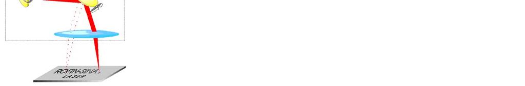

3 Background Principle of Laser Marking Galvo 3 HCHSU, ISU/Slide 3
4 Ultra-short Pulse Laser - Material Interaction Energy transfer from (pulsed) laser light to electrons (Absorption) After Electron-Phonon-Interaction-Time (EPIT) Energy transfer from Electrons to Phonons: Heat Ablation of material Absorption Heat Ablation 0 1 ps 100 ps 10 ns 1 µs Time HCHSU, ISU/Slide 4
5 Obtaining ps-pulses ps (and fs) Oscillators: Tens of MHz Repetition Rate (given by reson ator length) Laser Medium HCHSU, ISU/Slide 5

 HCHSU,")
6 Defining ultrafast fiber lasers is a tricky business, Tom Hausken HCHSU, ISU/Slide 6
7 Long pulse las er(>1ns) Pulse laser beam (Conventional) Ultra-short lase r(<10 ps) Ultra-hort pulse la ser beam Melted object s Debris Circuits (Damage) Little or no debris Circuits (no damage) Solidification layer Impulse wave Thin solidific ation layer Small micr o cracks (Large heat effect) Heat affected layer Micro crack Micro processing Small heat aff ected area Small amount of energy volume, High peak-power Processing with little or no heat affect, small micro crack s HCHSU, ISU/Slide 7 7
8 Key Parameters for Laser Machining power(w) repetition-rate(hz) defocus(mm) speed(mm/s) index(mm) HCHSU, ISU/Slide 8
9 Reciprocal Effects power - depth frequency - depth/surface debris defocus beam size speed surface ripple/debris index - overlap HCHSU, ISU/Slide 9
 4 ) 4-5um Low-k Silicon HCHSU,")
10 Low-k Wafer Structure 2 um Cu 1 um Cu-Seed 250A Ta(Tantalum) 500A TEOS (tetraethyl orthosilicate, Si(OC 2 H 5 ) 4 ) 4-5um Low-k Silicon HCHSU, ISU/Slide 10


11 Pattern HCHSU, ISU/Slide 11


12 Laser Machine Experimental Works HCHSU, ISU/Slide 12

")

13 Grooving on Cu-low K wafer (45nm<) street HCHSU, ISU/Slide 13

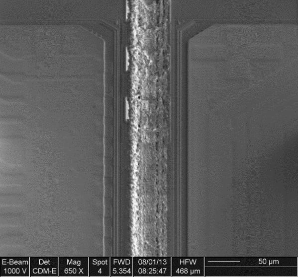
14 HCHSU, ISU/Slide 14


15 Repeatability Laser: 6M, spot size 17 μm with 5W. Speed: 550mm/s Top viewed and depth measured by SEM Result: No HAZ, Particles or Recast Channel Depth 6.02μm and Width 16.8 μm Test pads is not removed Cu Pad cross section 1-1 cross section Top view HCHSU, ISU/Slide 15

 Depth")

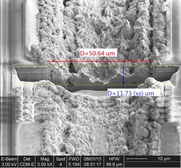
16 First Try of Overlap Scribing & 3D Confocal Microscopy(In May 2013) Power = 10W Speed = 300mm/s 2 passes overlap 100%(17um) Depth = um Width = 17um A A A A A-A Cross Section HCHSU, ISU/Slide 16
17 DOE---Taguchi Methods Factor Level 1 Level 2 Level 3 A 4MHz 6MHz 10MHz Repetition Rate B 5W 10W 15W Power C 150mm/s 300mm/s 600mm/s Speed D Passes 2 passes (overlap 20%) 2 passes (overlap 50%) 2 passes (overlap 100%) A B C D 1 L1 L1 L1 L1 2 L1 L2 L2 L2 3 L1 L3 L3 L3 4 L2 L1 L2 L3 5 L2 L2 L3 L1 6 L2 L3 L1 L2 7 L3 L1 L3 L2 8 L3 L2 L1 L3 9 L3 L3 L2 L1 HCHSU, ISU/Slide 17
18 No. Depth(um) Average(um)
19 Factor Level 1 Level 2 Level 3 A 4MHz 6MHz 10MHz Repetition Rate B 5W 10W 15W Power C 150mm/s 300mm/s 600mm/s Speed D Passes 2 passes (overlap 20%) 2 passes (overlap 50%) 2 passes (overlap 100%) A B C D Optimization:A1B3C3D3 (4MHz, 15W, 600mm/s, overlap 100%) HCHSU, ISU/Slide 19

20 Results Laser Grooving Item Specification Industrial Standard 1 Heat affect analysis(debris) < 5 μm 3.57μm Experimental Work 2 Top side chipping Not allow <0.005μm 3 Passivation peeling Not allow <0.005μm 4 Laser groove depth >10 μm μm 5 Wafer scratch Not allow <0.005μm 6 Die crack Not allow <0.005μm 7 Wafer broken Not allow None 8 Laser total kerf width Target ± 3um ± 2.73μm 9 Laser kerf shift ± 2um ± 1.96μm HCHSU, ISU/Slide 20
21 Item Specification Industrial Standard 1 Heat affect analysis(debris) < 5 μm 3.57μm Experimental Work 2 Top side chipping Not allow <0.005μm 3 Passivation peeling Not allow <0.005μm 4 Laser groove depth >10 μm μm 5 Wafer scratch Not allow <0.005μm 6 Die crack Not allow <0.005μm 7 Wafer broken Not allow None 8 Laser total kerf width Target ± 3um ± 2.73μm 9 Laser kerf shift ± 2um ± 1.96μm HCHSU, ISU/Slide 21
22 Recipe for 28 nm low-k wafer Stage Type Power(w) Frequency (khz) Index (um) Defocus (mm) Speed (mm/s) Laser Saw BSS6 1st 2.7 2nd 3.7 3rd 2.8 1st 200 2nd 40 3rd 60 1st 47 2nd 50 (mask) 3rd 50 (mask) 1st 0 2nd 0 3rd 0 1st 300 2nd 125 3rd 300 HCHSU, ISU/Slide 22

23 measure the dimension of laser grooving OM Photo Laser Profile HCHSU, ISU/Slide 23
24 quality index Index criteria Method Min. Max. Avg. STD. CPK Metal residue Not allow OM No Metal Residue Kerf width 55±5 um Debris top opening 50±5 um Debris bottom Laser Profile 42.5±7.5 um opening scanner Laser Depth 14±4 um Laser Debris <5um HCHSU, ISU/Slide 24


25 Sidewall void for 45 nm low-k wafer 1 ST 2 nd 3 rd 5 th 4 th 3,4 pa ss After Blade Saw(Normal) HCHSU, ISU/Slide 25
26 Laser Grooving Parameter Laser Grooving Pass Power (W) Frequency (khz) Speed (mm/s) Defocus (mm) Index (mm) DOE Kerf width DOE2 Kerf width 52 DOE3 Kerf width 47 1 NC NC NC NC NC NC NC NC NC NC NC NC NC NC NC NC NC NC NC NC 0 1 NC NC NC NC NC NC NC NC NC NC NC NC NC NC NC NC NC NC NC NC 0 NC : same as DOE1 HCHSU, ISU/Slide 26
27 Sawing street:64um Laser width:55um Z1 Kerf width 30~ 35um Index:0.024 Index: Index:0.009 Index: Index:0 DOE 1 HCHSU, ISU/Slide 27


28 Sawing street:64um Laser width:52um Z1 Kerf width 30~ 35um Index:0.022 Index: Index:0.007 Index: Index:0 DOE 2 HCHSU, ISU/Slide 28

29 Sawing street:64um Laser width:47um Z1 Kerf width 30~ 35um Index:0.02 Index:-0.02 Index:0.005 Index: Index:0 DOE 3 HCHSU, ISU/Slide 29

30 B A Backside view C D For all 4-side, only DOE 3 eliminate sidewall voids. HCHSU, ISU/Slide 30
31 Summary A 30W 10 ps green (515 nm) mode-lock ed fiber laser was successfully applied to 3D IC packaging. The cutting speed at 800mm/sec and 50 % of power can satisfy most of the requi rement. For laser grooving, excellent performance has been satisfied industrial standard. HCHSU, ISU/Slide 31

32 HCHSU, ISU/Slide 32
33 End of presentation Thank you for your attention! HCHSU, ISU/Slide 33
Enabling Technology in Thin Wafer Dicing
 Enabling Technology in Thin Wafer Dicing Jeroen van Borkulo, Rogier Evertsen, Rene Hendriks, ALSI, platinawerf 2G, 6641TL Beuningen Netherlands Abstract Driven by IC packaging and performance requirements,
Laser Dicing of Silicon: Comparison of Ablation Mechanisms with a Novel Technology of Thermally Induced Stress
 Dicing of Silicon: Comparison of Ablation Mechanisms with a Novel Technology of Thermally Induced Stress Oliver HAUPT, Frank SIEGEL, Aart SCHOONDERBEEK, Lars RICHTER, Rainer KLING, Andreas OSTENDORF Zentrum
Multi Beam Laser Grooving Process Parameter Development and Die Strength Characterization for 40nm Node Low-K/ULK Wafer
 Multi Beam Laser Grooving Process Parameter Development and Die Strength Characterization for 40nm Node Low-K/ULK Wafer Koh Wen Shi 1,3, K. Y. Yow 1, Calvin Lo 1, Dr. Yap Boon Kar 2, Dr. Halina Misran
Optimizing the processing of sapphire with ultrashort laser pulses
 Optimizing the processing of sapphire with ultrashort laser pulses Geoff Lott 1, Nicolas Falletto 1, Pierre-Jean Devilder, and Rainer Kling 3 1 Electro Scientific Industries, Eolite Systems, 3 Alphanov
PDF created with FinePrint pdffactory Pro trial version
 Benefits Damage-free dicing of thin silicon Capable of producing smallest street widths which in return provides additional space for more parts per wafer Single step process results in reduction of cost
Dr Jack Gabzdyl Product Line Manager Pulsed Lasers
 AILU PHOTONEX 08 16 th October 2008 Fiber Lasers for Medical Applications Dr Jack Gabzdyl Product Line Manager Pulsed Lasers General Advantages of Fibre Lasers Beam Quality & Stability Diffraction-limited
Lasers and Laser Systems for Micro-machining
 Lasers and Laser Systems for Micro-machining Martyn Knowles Oxford Lasers Ltd Unit 8, Moorbrook Park Didcot, Oxfordshire, OX11 7HP Tel: +44 (0) 1235 810088 www.oxfordlasers.com Lasers and Laser Systems
Influence of laser marking on stainless steel surface and corrosion resistance
 Lasers in Manufacturing Conference 2015 Influence of laser marking on stainless steel surface and corrosion resistance Martin Kučera a *, Michal Švantner a, Eva Smazalová a a, New Technologies - Research
Abstract. Introduction
 Accelerating Silicon Carbide Power Electronics Devices into High Volume Manufacturing with Mechanical Dicing System By Meng Lee, Director, Product Marketing and Jojo Daof, Senior Process Engineer Abstract
Introduction to Picosecond Laser Tutorial. CMC Laboratories, Inc.
 Introduction to Picosecond Laser Tutorial CMC Laboratories, Inc. Pico-second Ultra-short light pulses 1 picosecond is 10-12 seconds Light travels 300,000,000 meters per second, in 3 picoseconds it travels
Laser Micromilling :
 Laser Micromilling : An Enabling Technology for MicroComponent Replication Martyn Knowles Oxford Lasers Ltd. Unit 8, Moorbrook Park Didcot, Oxon OX11 7HP Tel: +44-1235-814433 Outline Introduction Process
High Yield Dicing of 100 mm and 150 mm SiC Wafer with High Throughput
 High Yield Dicing of 100 mm and 150 mm SiC Wafer with High Throughput Hans-Ulrich Zühlke (3D-Micromac, Chemnitz) Dirk Lewke (Fraunhofer IISB, Erlangen) Content 1. Motivation 2. Basics of TLS-Dicing 3.
Lasers in Advanced Packaging
 Lasers in Advanced Packaging Xiangyang Song, Cristian Porneala, Dana Sercel, Kevin Silvia, Joshua Schoenly, Rouzbeh Sarrafi, Sean Dennigan, Eric DeGenova, Scott Tompkins, Brian Baird, Vijay Kancharla,
CMP Scratches; Their Detection and Analysis on Root Causes
 6 th LEVITRONIX CMP and Ultrapure Conference The Westin Park Central, Dallas, Texas May 11-12, 2011 CMP Scratches; Their Detection and Analysis on Root Causes Jin-Goo Park May 11, 2011 Department of Materials
microdice System for Separation of SiC Wafer Using Thermal Laser Separation
 microdice System for Separation of SiC Wafer Using Thermal Laser Separation - System Integration Technologies Fraunhofer ENAS - (Ronny Neubert, 3D-Micromac AG) 3D-Micromac At a Glance Manufacturer and
Marking Cutting Welding Micro Machining Additive Manufacturing
 Marking Cutting Welding Micro Machining Additive Manufacturing Slide: 1 Nanosecond Laser Welding of Dissimilar Metals and Foils Daniel Capostagno, Adam Rosowski, Jack Gabzdyl, Michael Duka EPMT 2017 Geneva
Confocal Microscopy of Electronic Devices. James Saczuk. Consumer Optical Electronics EE594 02/22/2000
 Confocal Microscopy of Electronic Devices James Saczuk Consumer Optical Electronics EE594 02/22/2000 Introduction! Review of confocal principles! Why is CM used to examine electronics?! Several methods
EXAMPLES OF INDUSTRIAL APPLICATIONS
 14 EXAMPLES OF INDUSTRIAL APPLICATIONS STEEL FOIL Μ-DRILLING No melting Micron diameter Filters Functional surfaces DIAMOND CUTTING Low carbonization No HAZ Low material loss Diamond sheet cutting Chip
EXAMPLES OF INDUSTRIAL APPLICATIONS
 14 EXAMPLES OF INDUSTRIAL APPLICATIONS STEEL FOIL Μ-DRILLING No melting Micron diameter Filters Functional surfaces DIAMOND CUTTING Low carbonization No HAZ Low material loss Diamond sheet cutting Chip
Verfahrens- und Systemtechnik zum präzisen Hochleistungsabtrag mit UKP-Lasern
 Verfahrens- und Systemtechnik zum präzisen Hochleistungsabtrag mit UKP-Lasern Jens Holtkamp Motivation Ultra short pulsed lasers National Institute of Standards and Technology (NIST) Regional Laser and
Micromachining of metals and thermal barrier coatings using a 532 nm nanosecond fiber laser
 Available online at www.sciencedirect.com Physics Procedia 39 (01 ) 603 61 LANE 01 Micromachining of metals and thermal barrier coatings using a 53 nm nanosecond fiber laser Huan Qi, Hongkun Lai University
NSOP REDUCTION FOR QFN RFIC PACKAGES
 As originally published in the SMTA Proceedings NSOP REDUCTION FOR QFN RFIC PACKAGES Mumtaz Y. Bora Peregrine Semiconductor San Diego, CA, USA mbora@psemi.com ABSTRACT Wire bonded packages using conventional
Laser Micromachining of Bulk Substrates and Thin Films Celine Bansal
 Laser Micromachining of Bulk Substrates and Thin Films Celine Bansal Oxford Lasers Ltd Moorbrook Park Didcot, Oxfordshire, OX11 7HP Tel: +44 (0) 1235 810088 www.oxfordlasers.com Outline Oxford Lasers Importance
Joining dissimilar metals made possible with pulsed laser nano second welding
 Joining dissimilar metals made possible with pulsed laser nano second welding March 2018 Marking Cutting Welding Micro Machining Additive Manufacturing Slide: 1 02/10/2017 CM-F00003 Rev 6 Micro joining
Picosecond Laser Patterning of ITO Thin Films
 Available online at www.sciencedirect.com Physics Procedia 12 (2011) 133 140 LiM 2011 Picosecond Laser Patterning of ITO Thin Films Anna Risch*, Ralf Hellmann University of Applied Sciences Aschaffenburg,
Advantages of picosecond laser machining for cutting-edge technologies
 Available online at www.sciencedirect.com Physics Procedia 41 (2013 ) 381 388 Lasers in Manufacturing Conference 2013 Advantages of picosecond laser machining for cutting-edge technologies Abstract C.
NSOP Reduction for QFN RFIC Packages
 NSOP Reduction for QFN RFIC Packages Mumtaz Y. Bora Peregrine Semiconductor San Diego, CA mbora@psemi.com Abstract Wire bonded packages using conventional copper leadframe have been used in industry for
Improvement of Laser Fuse Processing of Fine Pitch Link Structures for Advanced Memory Designs
 Improvement of Laser Fuse Processing of Fine Pitch Link Structures for Advanced Memory Designs Joohan Lee, Joseph J. Griffiths, and James Cordingley GSI Group Inc. 60 Fordham Rd. Wilmington, MA 01887 jlee@gsig.com
Isolation Scribing on Hybrid Films for CIGS-Based Solar Cell Using Various Nanosecond Pulsed Laser Wavelengths
 Isolation Scribing on Hybrid Films for CIGS-Based Solar Cell Using Various Nanosecond Pulsed Laser Wavelengths Ming-Fei Chen *, Wen-Tse Hsiao **, Ming-Cheng Wang * and Ying-Fang Chen * * Department of
Laser Processes for Micro and Nano Scale Functionalisation of Surfaces
 Laser Processes for Micro and Nano Scale Functionalisation of Surfaces Claudia Hartmann Sebastian Theiß, Fritz Klaiber, Arnold Gillner Hannover, 21.04.2010 Outline Functional structures examples from nature
Customizing Processes for Hermetic Assembly Of Devices Designed for Plastic Packages (1 of 3)
") Customizing Processes for Hermetic Assembly Of Devices Designed for Plastic Packages (1 of 3) Charlie C. Megia Golden Altos Corporation 402 South Hillview Drive, Milpitas, CA 95035 cmegia@goldenaltos.com
Customizing Processes for Hermetic Assembly Of Devices Designed for Plastic Packages (1 of 3) Charlie C. Megia Golden Altos Corporation 402 South Hillview Drive, Milpitas, CA 95035 cmegia@goldenaltos.com
Enhancement Mode GaN FETs and ICs Visual Characterization Guide
 Enhancement Mode GaN FETs and ICs Visual Characterization Guide EFFICIENT POWER CONVERSION Alana Nakata, Vice President, Product Engineering, Efficient Power Conversion Corporation A detailed description
Dallas Semicoductor DS80C320 Microcontroller
 Construction Analysis Dallas Semicoductor DS80C320 Microcontroller Report Number: SCA 9702-525 Global Semiconductor Industry the Serving Since 1964 15022 N. 75th Street Scottsdale, AZ 85260-2476 Phone:
Laser Micromachining for Industrial Applications and R&D. 3D-Micromac AG. Symposium on Smart Integrated Systems in Chemnitz. 3D-Micromac AG
 3D-Micromac AG Symposium on Smart Integrated Systems in Chemnitz 1 1 microdice - TLS-Dicing for separation of SiC 2 microprep - for high-throughput microstructure diagnostics 3 About 3D-Micromac AG 2 microdice
Analysis of Laser Ablation of CFRP by Ultra-Short Laser Pulses with Short Wavelength
 Available online at www.sciencedirect.com Physics Procedia 12 (2011) 565 571 LiM 2011 Analysis of Laser Ablation of CFRP by Ultra-Short Laser Pulses with Short Wavelength C. Emmelmanna, M. Petersen, A.
TSV Processing and Wafer Stacking. Kathy Cook and Maggie Zoberbier, 3D Business Development
 TSV Processing and Wafer Stacking Kathy Cook and Maggie Zoberbier, 3D Business Development Outline Why 3D Integration? TSV Process Variations Lithography Process Results Stacking Technology Wafer Bonding
LOW TEMPERATURE PHOTONIC SINTERING FOR PRINTED ELECTRONICS. Dr. Saad Ahmed XENON Corporation November 19, 2015
 LOW TEMPERATURE PHOTONIC SINTERING FOR PRINTED ELECTRONICS Dr. Saad Ahmed XENON Corporation November 19, 2015 Topics Introduction to Pulsed Light Photonic sintering for Printed Electronics R&D Tools for
FABRICATION AND RELIABILITY OF ULTRA-FINE RDL STRUCTURES IN ADVANCED PACKAGING BY EXCIMER LASER ABLATION
 FABRICATION AND RELIABILITY OF ULTRA-FINE RDL STRUCTURES IN ADVANCED PACKAGING BY EXCIMER LASER ABLATION NCCAVS Joint Users Group Technical Symposium San Jose, June 7 th, 2017 Markus Arendt, SÜSS MicroTec
Micro Patterning of Crystalline Structures on a-ito Films on Plastic Substrates Using Femtosecond Laser
 Technical Communication JLMN-Journal of Laser Micro/Nanoengineering Vol. 4, No. 3, 2009 Micro Patterning of Crystalline Structures on a-ito Films on Plastic Substrates Using Femtosecond Laser Chung-Wei
Advanced Manufacturing Choices
 Advanced Manufacturing Choices Table of Content Mechanical Removing Techniques Ultrasonic Machining (USM) Sputtering and Focused Ion Beam Milling (FIB) Ultrasonic Machining In ultrasonic machining (USM),
Rapid Microtooling with laser based methods
 Hochschule Mittweida University of Applied Sciences Rapid Microtooling with laser based methods R. Ebert, U. Löschner, A. Streek, J. Schille, T. Süß, L. Hartwig, U. Klötzer, H. Exner ISL 2008 Chemnitz
UMC UM F-7 2M-Bit SRAM
 Construction Analysis UMC UM 613264F-7 2M-Bit SRAM Report Number: SCA 9609-511 Global Semiconductor Industry the Serving Since 1964 15022 N. 75th Street Scottsdale, AZ 85260-2476 Phone: 602-998-9780 Fax:
Femtosecond Laser Materials Processing. B. C. Stuart P. S. Banks M. D. Perry
 UCRL-JC-126901 Rev 2 PREPRINT Femtosecond Laser Materials Processing B. C. Stuart P. S. Banks M. D. Perry This paper was prepared for submittal to the Manufacturing '98 Chicago, IL September 9-16, 1998
Water Jet Guided Laser Cutting of Silicon Thin Films Using 515nm Disk Laser
 Technical Communication JLMN-Journal of Laser Micro/Nanoengineering Vol. 6, No. 2, 11 Water Jet Guided Laser Cutting of Silicon Thin Films Using 515nm Disk Laser Eva-Maria Heilmann*, Albrecht Seidl** and
Precision Glass Processing with Pico-second Laser Pulses. Chemically Strengthened Glasses. Structure
 Precision Glass Processing with Pico-second Laser Pulses Mathew Rekow, Yun Zhou and Nicolas Falletto Mechanical scribe and break, grinding and sawing have been mainstays of glass processing for centuries.
High Density Perforation of Thin Al-Foils with Ultra Short Pulse Lasers in Dependence on the Repetition Rate
 High Density Perforation of Thin Al-Foils with Ultra Short Pulse Lasers in Dependence on the Repetition Rate Nelli Hambach *1, Claudia Hartmann *1,2, Stephan Keller *1, Arnold Gillner *1,2 *1 Fraunhofer
EXPERIMENTAL STUDIES ON FIBRE LASER MICRO-MACHINING OF Ti-6Al-4V.
 EXPERIMENTAL STUDIES ON FIBRE LASER MICRO-MACHINING OF Ti-6Al-4V. A. SEN 1*, B. DOLOI 2, B.BHATTACHARYYA 3 1* PRODUCTION ENGINEERING DEPARTMENT, JADAVPUR UNIVERSITY, KOLKATA, INDIA, 700032, Email: abhishek.sen1986@gmail.com
EFFICIENCY AND PRODUCTIVITY INCREASE OF SOLAR-CELLS AND -MODULES BY INNOVATIVE LASER APPROACHES
 EFFICIENCY AND PRODUCTIVITY INCREASE OF SOLAR-CELLS AND -MODULES BY INNOVATIVE LASER APPROACHES PD Dr. Alexander Horn, V. Schütz, J. Gonzalez, C.C. Kalmbach Photovoltaics Group Dpt. for Production and
Selective front side patterning of CZTS thin-film solar cells by picosecond laser induced material lift-off process
 Available online at www.sciencedirect.com Physics Procedia 41 (2013 ) 741 745 Lasers in Manufacturing Conference 2013 Selective front side patterning of CZTS thin-film solar cells by picosecond laser induced
High Throughput Laser Processing of Guide Plates for Vertical Probe Cards Rouzbeh Sarrafi, Dana Sercel, Sean Dennigan, Joshua Stearns, Marco Mendes
 High Throughput Laser Processing of Guide Plates for Vertical Probe Cards Rouzbeh Sarrafi, Dana Sercel, Sean Dennigan, Joshua Stearns, Marco Mendes IPG Photonics - Microsystems Division Outline Introduction
Motorola MPA1016FN FPGA
 Construction Analysis Motorola MPA1016FN FPGA Report Number: SCA 9711-561 Global Semiconductor Industry the Serving Since 1964 17350 N. Hartford Drive Scottsdale, AZ 85255 Phone: 602-515-9780 Fax: 602-515-9781
Chips Face-up Panelization Approach For Fan-out Packaging
 Chips Face-up Panelization Approach For Fan-out Packaging Oct. 15, 2015 B. Rogers, D. Sanchez, C. Bishop, C. Sandstrom, C. Scanlan, TOlson T. REV A Background on FOWLP Fan-Out Wafer Level Packaging o Chips
Femtosecond micromachining in polymers
 Femtosecond micromachining in polymers Prof. Dr Cleber R. Mendonca Daniel S. Corrêa Prakriti Tayalia Dr. Tobias Voss Dr. Tommaso Baldacchini Prof. Dr. Eric Mazur fs-micromachining focus laser beam inside
Cost Effective 3D Glass Microfabrication for Advanced Packaging Applications
 Cost Effective 3D Glass Microfabrication for Advanced Packaging Applications Authors: Jeb. H Flemming, Kevin Dunn, James Gouker, Carrie Schmidt, Roger Cook ABSTRACT Historically, while glasses have many
Chapter 4 Fabrication Process of Silicon Carrier and. Gold-Gold Thermocompression Bonding
 Chapter 4 Fabrication Process of Silicon Carrier and Gold-Gold Thermocompression Bonding 4.1 Introduction As mentioned in chapter 2, the MEMs carrier is designed to integrate the micro-machined inductor
Micron Semiconductor MT5C64K16A1DJ 64K x 16 SRAM
 Construction Analysis Micron Semiconductor MT5C64K16A1DJ 64K x 16 SRAM Report Number: SCA 9412-394 Global Semiconductor Industry the Serving Since 1964 17350 N. Hartford Drive Scottsdale, AZ 85255 Phone:
Investigations on Melting and Welding of Glass by Ultra-short Laser Radiation
 Investigations on Melting and Welding of Glass by Ultra-short Laser Radiation Alexander HORN *, Ilja MINGAREEV * and Alexander WERTH * * Lehrstuhl für Lasertechnik, Rheinisch-Westfälische Technische Hochschule
Experimental Study on Micromachining of 304 Stainless Steel Under Water Using Pulsed Nd:YAG Laser Beam
 5 th International & 26 th All India Manufacturing Technology, Design and Research Conference (AIMTDR 2014) December 12 th 14 th, 2014, IIT Guwahati, Assam, India Experimental Study on Micromachining of
VTC VM365830VSJ Pre-Amp
 Construction Analysis VTC VM365830VSJ Pre-Amp Report Number: SCA 9708-549 Global Semiconductor Industry the Serving Since 1964 17350 N. Hartford Drive Scottsdale, AZ 85255 Phone: 602-515-9780 Fax: 602-515-9781
Development of Cleanliness Specification of Receptacle Transceivers: Fiber Stub
 Development of Cleanliness Specification of Receptacle Transceivers: Fiber Stub Ryo Nagase : Chiba Institute of Technology Hideki Isono : Fujitsu Optical Components Ltd. Yutaka Sadohara : Sumitomo electric
TSV Interposer Process Flow with IME 300mm Facilities
 TSV Interposer Process Flow with IME 300mm Facilities Property of Institute of Microelectronics (IME)-Singapore August 17, 2012 Outline 1. TSV interposer (TSI) cross sectional schematic TSI with BEOL,
Rockwell R RF to IF Down Converter
 Construction Analysis Rockwell R6732-13 RF to IF Down Converter Report Number: SCA 9709-552 Global Semiconductor Industry the Serving Since 1964 17350 N. Hartford Drive Scottsdale, AZ 85255 Phone: 602-515-9780
Embedding of Active Components in LCP for Implantable Medical Devices
 44 th IMAPS New England Symposium 2017 Embedding of Active Components in LCP for Implantable Medical Devices Dr. Eckardt Bihler and Dr. Marc Hauer, Dyconex AG Susan Bagen, PE, Micro Systems Technologies,
Laser Cutting of Electrodes for Advanced Batteries
 Proceedings of LPM2010 - the 11th International Symposium on Laser Precision Microfabrication Laser Cutting of Electrodes for Advanced Batteries Hans J. HERFURTH, Rahul PATWA and Henrikki PANTSAR Fraunhofer
LASER TECHNOLOGY IN SURFACE TREATMENT
 TRUMPF Nederland B.V. LASER TECHNOLOGY IN SURFACE TREATMENT The Next Industrial Level Gert van Wakeren Sales Engineer Laser Technology Scherpenzeel, 1-11-2017 1 Agenda 1. About TRUMPF 2. Introduction laser
Optical Components: Laser Crystals
 Optical Components: Laser Crystals Table of Contents Crystals Introduction... 2 Nd: YVO 4... 3 Nd:YAG... 6 Nd:YLF... 7 Cr:YAG... 9 1 Crystals Introduction Sinoceramics supplies many types of crystals for
DEPTH SELECTIVE LASER SCRIBING OF THIN-FILM SILICON SOLAR CELLS ON FOIL Paper M1106
 DEPTH SELECTIVE LASER SCRIBING OF THIN-FILM SILICON SOLAR CELLS ON FOIL Paper M116 Laurie Wipliez 1*, Jochen Löffler 1, Martijn de Keijzer 1, Wim Soppe 1, Thomas Sebastien 1 Aart Schoonderbeek 2, Oliver
In-process Monitoring and Adaptive Control during Micro Welding with CW Fiber Laser
 In-process Monitoring and Adaptive Control during Micro Welding with CW Fiber Laser Yousuke KAWAHITO*, Masaharu KAWASAKI* and Seiji KATAYAMA* * Osaka University, Joining and Welding Research Institute
Hitachi A 64Mbit (8Mb x 8) Dynamic RAM
 Dynamic RAM") Construction Analysis Hitachi 5165805A 64Mbit (8Mb x 8) Dynamic RAM Report Number: SCA 9712-565 Global Semiconductor Industry the Serving Since 1964 17350 N. Hartford Drive Scottsdale, AZ 85255 Phone:
Construction Analysis Hitachi 5165805A 64Mbit (8Mb x 8) Dynamic RAM Report Number: SCA 9712-565 Global Semiconductor Industry the Serving Since 1964 17350 N. Hartford Drive Scottsdale, AZ 85255 Phone:
Advances in Intense Pulsed Light Solutions For Display Manufacturing. XENON Corporation Dr. Saad Ahmed Japan IDW 2016
 Advances in Intense Pulsed Light Solutions For Display Manufacturing XENON Corporation Dr. Saad Ahmed Japan IDW 2016 Talk Outline Introduction to Pulsed Light Applications in Display UV Curing Applications
Challenges in Material Applications for SiP
 Challenges in Material Applications for SiP Sze PeiLim Regional Product Manager for Semiconductor Products Indium Corporation Indium Corporation Materials Supplier: SMT solder pastes and fluxes Power semiconductor
Laser Micromachining of Coated YBa 2 Cu 3 O 6+x Superconducting Thin Films
 Laser Micromachining of Coated YBa 2 Cu 3 O 6+x Superconducting Thin Films Principle Author: Kenneth E. Hix, Mound Laser & Photonics Center, Inc., P.O. Box 223, Miamisburg, OH 45343, 937-865-3041, 937-865-3680
Femtosecond laser pre-pulse technology for LPP EUV source
 Femtosecond laser pre-pulse technology for LPP EUV source A. Vinokhodov*, V. Krivtsun*, **, M.Krivokorytov*, Yu. Sidelnikov*, **, S.Chekalin**, V.Kompanets**, A. Melnikov**, K. Koshelev*, ** * EUV Labs,
Application of disc lasers in Medical device manufacturing
 Application of disc lasers in Medical device manufacturing Ramasamy Elavarasan, Peter Jepsen Jan Scheftlein * Prosint, 2220 Oakland Road, San Jose, CA 96131, USA * Prenovatec GmbH, Nachtigallenstr, 13
Oki M A-60J 16Mbit DRAM (EDO)
") Construction Analysis Oki M5117805A-60J 16Mbit DRAM (EDO) Report Number: SCA 9707-545 Global Semiconductor Industry the Serving Since 1964 17350 N. Hartford Drive Scottsdale, AZ 85255 Phone: 602-515-9780
Construction Analysis Oki M5117805A-60J 16Mbit DRAM (EDO) Report Number: SCA 9707-545 Global Semiconductor Industry the Serving Since 1964 17350 N. Hartford Drive Scottsdale, AZ 85255 Phone: 602-515-9780
SGS-Thomson M17C1001 1Mb UVEPROM
 Construction Analysis SGS-Thomson M17C1001 1Mb UVEPROM Report Number: SCA 9612-518 Global Semiconductor Industry the Serving Since 1964 15022 N. 75th Street Scottsdale, AZ 85260-2476 Phone: 602-998-9780
Fabrication of Micro and Nano Structures in Glass using Ultrafast Lasers
 Fabrication of Micro and Nano Structures in Glass using Ultrafast Lasers Denise M. Krol University of California, Davis IMI Glass Workshop Washington DC April 15-17, 2007 Femtosecond laser modification
Monocrystalline Silicon Wafer Specification (Off-spec)
") Monocrystalline Silicon Wafer Specification (Off-spec) General information: o Product: Wafer o Code: n-125-166f-f180µ o Version date: 2011-10-06 Key characteristics: o Czochralski grown o n-type o 125.25
Monocrystalline Silicon Wafer Specification (Off-spec) General information: o Product: Wafer o Code: n-125-166f-f180µ o Version date: 2011-10-06 Key characteristics: o Czochralski grown o n-type o 125.25
Marking Decorative Features to Stainless Steel with Fiber Laser
 Marking Decorative Features to Stainless Steel with Fiber Laser Petri Laakso, Ville Mehtälä VTT Technical Research Centre of Finland Henrikki Pantsar Fraunhofer Color marking on stainless steel has been
Assembling Ordered Nanorod Superstructures and Their Application as Microcavity Lasers
 Supporting Information Assembling Ordered Nanorod Superstructures and Their Application as Microcavity Lasers Pai Liu 1, Shalini Singh 1, Yina Guo 2, Jian-Jun Wang 1, Hongxing Xu 3, Christophe Silien 4,
Microelectronics Reliability
 Microelectronics Reliability 52 (2012) 2627 2631 Contents lists available at SciVerse ScienceDirect Microelectronics Reliability journal homepage: www.elsevier.com/locate/microrel Investigation on CDM
SGS-Thomson M28C K EEPROM
 Construction Analysis SGS-Thomson M28C64-121 64K EEPROM Report Number: SCA 9710-559 Global Semiconductor Industry the Serving Since 1964 17350 N. Hartford Drive Scottsdale, AZ 85255 Phone: 602-515-9780
Shaped Femtosecond Laser Pulse Spectroscopy for Nuclear Forensics. Phyllis Ko ANS Student Conference 2011
 Shaped Femtosecond Laser Pulse Spectroscopy for Nuclear Forensics Phyllis Ko ANS Student Conference 2011 Nuclear Forensics Analyzing nuclear material recovered from unused, intercepted devices or post-detonation
1 mw/[] Bond-Able Post-Passivation Interconnect for Power Management Technologies.
![1 mw/[] Bond-Able Post-Passivation Interconnect for Power Management Technologies.](/thumbs/96/129184811.jpg "1 mw/[] Bond-Able Post-Passivation Interconnect for Power Management Technologies.") 1 mw/[] Bond-Able Post-Passivation Interconnect for Power Management Technologies. Alexander Kalnitsky, Y.W. Tseng, T.H. Chien, C.Y. Chang, Felix Tsui 1 Outline Technology development Planarized passivation
1 mw/[] Bond-Able Post-Passivation Interconnect for Power Management Technologies. Alexander Kalnitsky, Y.W. Tseng, T.H. Chien, C.Y. Chang, Felix Tsui 1 Outline Technology development Planarized passivation
ANALYSING BACKSIDE CHIPPING ISSUES OF THE DIE AT WAFER SAW. Martin Vagues In Partial Fulfillment of MatE 234 May 10th, 2003
 ANALYSING BACKSIDE CHIPPING ISSUES OF THE DIE AT WAFER SAW Martin Vagues In Partial Fulfillment of MatE 234 May 10th, 2003 Prof Gunaselvaduray SJSU, San Jose ABSTRACT With shrinking technologies evolving,
11.3 Polishing with Laser Radiation
 196 E. Willenborg 11.3 Polishing with Laser Radiation Edgar Willenborg The surface roughness of a part or product strongly influences its properties and functions. Among these can be counted abrasion and
Wafer Level Molded DDFN Package Project Duane Wilcoxen
 Wafer Level Molded DDFN Package Project Duane Wilcoxen Definition of DDFN (Encapsulated CSP) DDFN package basically is a CSP device with an epoxy coating on all (or most) of the device sides for added
Intel Pentium Processor W/MMX
 Construction Analysis Intel Pentium Processor W/MMX Report Number: SCA 9706-540 Global Semiconductor Industry the Serving Since 1964 15022 N. 75th Street Scottsdale, AZ 85260-2476 Phone: 602-998-9780 Fax:
Table 1. Chemical and Structural Properties. About 1095 C g/cm 3 1.2W/m/K( c); 1.6W/m/K(//c)
; 1.6W/m/K(//c)") CASTECH R NLO Crystals Beta-Barium Borate (β-bab 2 O 4 or BBO) Introduction Beta-Barium Borate (β-bab 2 O 4 or BBO), discovered and developed by FIRSM, CAS (Fujian Institute of Research on the Structure
CASTECH R NLO Crystals Beta-Barium Borate (β-bab 2 O 4 or BBO) Introduction Beta-Barium Borate (β-bab 2 O 4 or BBO), discovered and developed by FIRSM, CAS (Fujian Institute of Research on the Structure
SiC Backside Via-hole Process For GaN HEMT MMICs Using High Etch Rate ICP Etching
 SiC Backside Via-hole Process For GaN HEMT MMICs Using High Etch Rate ICP Etching Naoya Okamoto, Toshihiro Ohki, Satoshi Masuda, Masahito Kanamura, Yusuke Inoue, Kozo Makiyama, Kenji Imanishi, Hisao Shigematsu,
Laser Polishing of Metals. Fraunhofer Institute for Laser Technology ILT Steinbachstraße Aachen (Germany)
") Laser Polishing of Metals Fraunhofer Institute for Laser Technology ILT Steinbachstraße 15 52074 Aachen (Germany) https://www.ilt.fraunhofer.de Content 1 2 3 Laser Polishing of Metals - Basics 3D Laser
Laser Polishing of Metals Fraunhofer Institute for Laser Technology ILT Steinbachstraße 15 52074 Aachen (Germany) https://www.ilt.fraunhofer.de Content 1 2 3 Laser Polishing of Metals - Basics 3D Laser
Fs- Using Ultrafast Lasers to Add New Functionality to Glass
 An IMI Video Reproduction of Invited Lectures from the 17th University Glass Conference Fs- Using Ultrafast Lasers to Add New Functionality to Glass Denise M. Krol University of California, Davis 17th
Challenges and Future Directions of Laser Fuse Processing in Memory Repair
 Challenges and Future Directions of Laser Fuse Processing in Memory Repair Bo Gu, * T. Coughlin, B. Maxwell, J. Griffiths, J. Lee, J. Cordingley, S. Johnson, E. Karagiannis, J. Ehrmann GSI Lumonics, Inc.
Fabrication of micro/nano structures in glass by lasers
 Lehigh University Lehigh Preserve International Workshop on Scientific Challenges for Glass Research Glass Conferences and Workshops Spring 4-1-2007 Fabrication of micro/nano structures in glass by lasers
Advances in Welding and Joining Technologies Dr. Swarup Bag Department of Mechanical Engineering Indian Institute of Technology, Guwahati
 Advances in Welding and Joining Technologies Dr. Swarup Bag Department of Mechanical Engineering Indian Institute of Technology, Guwahati Lecture 15 Micro and Nano Joining Processes Part II Hello everybody,
Keywords: Copper (Cu101), Aluminum (Al 1100), average laser power (P avg ), pulse repetition rate (f p ), pulse width (t p )
, Aluminum (Al 1100), average laser power (P avg ), pulse repetition rate (f p ), pulse width (t p )") Laser Micro Welding of Dissimilar Material of Aluminum and Copper Alloys Z. Mohid a, M. A. A. Rosely b, N. H. Rafai c, M. Z. Rahim d, M. Rasidi Ibrahim e, E. A. Rahim f Precision Machining Research Center
Laser Micro Welding of Dissimilar Material of Aluminum and Copper Alloys Z. Mohid a, M. A. A. Rosely b, N. H. Rafai c, M. Z. Rahim d, M. Rasidi Ibrahim e, E. A. Rahim f Precision Machining Research Center
Supporting On-line Materials
 Supporting On-line Materials Conformational Analysis of DNA Repair Intermediates by Time-Resolved Fluorescence Spectroscopy Su Lin 1, David P. Horning 2, Jack W. Szostak 2, and John C. Chaput* 1 1 Center
Investigation of Recast Layer Formed on Titanium Alloy Machined by Wire Electric Discharge Machining
 IJIRST International Journal for Innovative Research in Science & Technology Volume 3 Issue 04 September 2016 ISSN (online): 2349-6010 Investigation of Recast Layer Formed on Titanium Alloy Machined by
XBSC/UBDC/UBSC/BBSC/ULSC 100 µm & 400 µm - Assembly by soldering
 Assembly by soldering General description This document describes the attachment techniques recommended by Murata* for their pre-bumped and un-bumped silicon capacitors on the customer substrates. This
Method For Stripping Copper In Damascene Interconnects >>>CLICK HERE<<<
 Method For Stripping Copper In Damascene Interconnects Damascene, or acid copper plating baths, have been in use since the mid 19th century on decorative items and machinery.1,2 The process generally uses